1. The PowderMEMS Process
1.1. General Description of the Process and Its Features
The PowderMEMS process comprises three key steps: dry filling of molds with microfine powder, subsequent solidification of the powder via ALD, and conditioning of the substrate for further processing
[1].
Figure 1 schematically depicts these steps. Starting materials are planar substrates—e.g., silicon or glass wafers—with pre-structured micro-molds and a dry powder of micron-sized particles of the filling material of choice.
Figure 1. Illustration of the PowderMEMS process
[1] by schematic drawings (
top) and corresponding SEM micrographs of real samples, obtained from NdFeB powder (
bottom): (
a) Dry-filled micro-molds with particles. (
b) Solidification of the powder bed via ALD. The blue layer in the drawing represents the ALD layer (not to scale). The surrounding substrate is not shown for clarity. In the SEM micrograph the particles (NdFeB) appear bright grey, while the surrounding ALD layer (75 nm Al
2O
3) is dark grey. (
c) Removal of excess particles from the substrate surface to enable post-processing in a cleanroom environment.
In the first step, the molds are filled with the dry particles, as illustrated in
Figure 1a. The utilization of dry particles in combination with a dedicated filling technique
[2] ensures a dense and reproducible filling of molds with lateral dimensions from 20 µm up to 4000 µm, and a depth of up to 1000 µm. However, due to its particulate nature, it is not possible to produce structures with a fill factor of 100% using PowderMEMS. Depending on the application, this might either be an advantage (e.g., microfluidics) or a drawback when compared to bulk material (e.g., mechanical stability).
In the second step, the loose particles are subjected to a low-temperature ALD process, as depicted in Figure 1b. Since the gaseous ALD precursors penetrate the voids between neighboring particles, the growing ALD layer homogeneously coats all particles in the particle bed, as well as the inner and outer surfaces of the mold. Neighboring particles are thus connected to one another at the points of contact, forming a mechanically stable porous 3D microstructure throughout the entire mold volume. Note that at this point in the process the structure remains embedded within the substrate, but can be released from the mold using an appropriate etching method (Figure 1b).
In the third and final step, the substrate with the integrated PowderMEMS structures is conditioned to enable further post-processing in a (MEMS-) cleanroom environment. The conditioning comprises the removal of excess particles from the surface of the substrate, as depicted in Figure 1c.
Since ALD is performed at comparatively low temperatures, the PowderMEMS procedure can be applied to a broad variety of powders. Solidification with Al
2O
3 is, for example, possible at temperatures between 75 °C and 300 °C via thermal ALD, using TMA and H
2O as precursors
[3]. Apart from Al
2O
3, solidification has already been demonstrated with SiO
2 at 300–350 °C using SIBDEA and ozone
[4]. High-aspect-ratio thermal ALD is available for other metal oxides—such as TiO
2, V
2O
5, and ZnO—nitrides, and metals
[5], yielding numerous ALD/powder material combinations for functional PowderMEMS structures.
Another advantage is that substrates incorporating PowderMEMS microstructures are compatible with common BEOL and MEMS production environments, and can be post-processed using standard processes of MEMS and semiconductor technology
[1][6]. As solidification via ALD is performed at comparatively low temperatures, the stresses between the substrate and the 3D microstructures remain low compared to high-temperature processes such as sintering. Since no pressure is applied to the particle bed during solidification, the mold dimensions are reproduced with high precision, without shrinkage of the PowderMEMS structure. The ALD layer envelops each particle, thus protecting them efficiently from the surrounding process or application environment. Since no organic materials are involved in the PowderMEMS procedure, the 3D microstructures exhibit excellent thermal stability, surviving temperatures up to 425 °C without degradation
[7]. To illustrate the integrability of the PowderMEMS procedure in MEMS processes,
Figure 2 displays a piezoelectric vibrational energy harvester featuring an array of permanent micromagnets fabricated from NdFeB powder at the wafer level.
Figure 2. (a) Top side of a piezoelectric energy harvester with permanent wafer-level integrated NdFeB magnets (black pixels). (b) Bottom of the silicon cantilever exhibiting the magnetic PowderMEMS structures. Each magnetic pixel is 180 × 180 × 500 µm3 in size.
1.2. Implementation of the PowderMEMS Process at Fraunhofer ISIT
Successful utilization of PowderMEMS structures in industrially relevant microsystems requires a sufficiently high level of technological maturity. For the PowderMEMS process, this especially demands the following:
- That all processes are automated, and allow for a sufficient throughput for mass production;
- That the processes are reproducible, with low variation across individual substrates, as well as from substrate to substrate;
- That non-destructive and fast characterization and process control methods are available at the substrate level;
- That the substrates can be appropriately conditioned to allow for post-processing in a common BEOL-compatible cleanroom environment after embedding the 3D microstructures.
Figure 3 illustrates how PowderMEMS microstructures are currently integrated on 8-inch silicon substrates at Fraunhofer ISIT. After creating the micro-mold pattern via DRIE in the MEMS cleanroom, the substrates are transferred into a dedicated laboratory. Here, the dry-filling procedure, the solidification via ALD, and part of the substrate conditioning are performed. The photoresist mask used for mold etching remains on the wafer as a sacrificial layer.
Figure 3. Schematic illustration of the realization of embedded functional 3D microstructures on 8-inch Si substrates, as implemented at Fraunhofer ISIT. All process steps are carried out using automated equipment, enabling industrially relevant manufacturing.
For filling of the micro-molds with particles, a novel automated procedure has been developed
[2]. The powder is dry-filled into the cavities using a combination of low-frequency and ultrasound vibration, in conjunction with mechanical compacting of the powder. With this procedure, molds with dimensions down to 10 micrometers can be filled reproducibly. Excess powder is removed from the wafer surface with an automated squeegee.
Subsequently, the substrates are transferred into the ALD tool (Picosun R3000B), in which the loose particles are agglomerated into rigid microstructures. The wafers are placed horizontally within the reaction chamber to prevent the loose powder from falling out of the molds before solidification. Currently, six 8-inch wafers can be processed in a single batch. Deposition of 75 nm Al
2O
3 at 75 °C has proven to be a suitable solidification layer for various applications
[1].
As the corresponding cross-sections in
Figure 3 illustrate, some excess particles remain on the substrate surface on the front side of the substrate, as well as on its backside, after mold filling. During the subsequent agglomeration process, these particles are fixed firmly to the substrate surface by the ALD solidification layer. Therefore, substrate conditioning is carried out after the ALD process. Bottom-side cleaning is performed by grinding and polishing with an automatic grinder (Disco DFG8540), as previously described in
[6]. Approximately 25 µm of silicon is typically removed from the bottom side of the substrates. For front-side conditioning, the photoresist mask left after DRIE is used as a sacrificial layer. After transfer of the substrates into the cleanroom, the photoresist is removed by O
2 plasma etching (Tepla barrel asher), followed by lift-off in an organic solvent and a final high-velocity spray clean (SSEC 3000 automatic spin etcher)
[6].
After surface conditioning, the substrates can be further processed in the cleanroom if required. As already mentioned, wafers with embedded PowderMEMS microstructures are BEOL-compatible, i.e., wafer processing can be implemented on common cleanroom equipment without major process changes at process temperatures up to 425 °C. For example, to finalize the piezoelectric vibrational energy harvester shown in
Figure 2 after micromagnet integration, post-processing includes various thin-film depositions as well as wet and dry etching of metals, dielectrics, and silicon
[8].
For magnetization of integrated magnetic structures, a custom-built wafer-level magnetization tool (MAGSYS, Dortmund, Germany) is available, which provides magnetic fields of up to 3.5 T across a whole 8-inch wafer. After loading the wafer to the tool, the substrate is automatically positioned within a coil. Subsequently, a current of up to 5.6 kA is passed through the coil for generation of the magnetic field.
1.3. Process Control
Appropriate methods to control process quality and to support process development are central to the successful use of PowderMEMS for innovative microsystems in both research and production. NdFeB-based micromagnets have proven to be suitable as test structures for process characterization. Vibrating-sample magnetometer (VSM) measurements can be utilized to monitor the reproducibility of the PowderMEMS processes—i.e., micro-mold filling and agglomeration
[2]—as well as for overall process development
[7][6]. Since NdFeB is very sensitive to oxygen and water vapor, the magnetic properties precisely reflect degradation effects pertaining to the particles or the Al
2O
3 ALD layer during post-processing. Of particular interest are the remanence B
r and the intrinsic coercivity H
ci. Since B
r depends on the amount of magnetic material, this value represents a measure of the mold-filling quality. H
ci is an intrinsic material property, and does not depend on the volume of a magnet. Deviating values of B
r and H
ci indicate an incomplete solidification of the particles or a degradation of the magnetic material due to manufacturing processes
[7].
However, VSM measurements are comparatively slow, and necessitate dicing of the substrate into chips. For in-line process monitoring, non-destructive test methods are needed. Qualitative magnetic field measurements with sufficient lateral resolution at the wafer level can be performed by means of magneto-optical microscopy. With this measurement technique, an optical contrast based on the local magnetization is generated due to the Faraday effect. In this way, a non-destructive, fast, and automated optical and magnetic quality control within the process chain can be realized. Figure 4a,b display optical and magneto-optical images, respectively, of integrated NdFeB PowderMEMS microstructures. The images were acquired after wafer-level magnetization at 3.5 T. The resolution in magneto-optical mode is sufficient to resolve magnetic structures with lateral dimensions of 125 µm, as shown in Figure 4c. The qualitative magnetic contrast and optical inspection, including 3D topologies, enable automated and rapid quality control within the process chain, along with identification of defective magnetic microstructures.
Figure 4. (a) Optical image of NdFeB microstructures embedded in a silicon substrate. (b) The same structures imaged with a magneto-optical sensor based on the Faraday effect. The contrast corresponds to the strength of the out-of-plane component of the magnetic field. (c) Magneto-optical image of the ROI marked by a dashed frame in (b), acquired at higher magnification with a different lens.
Depending on the application requirements, and to ensure process stability, quantitative characterization of magnetic microstructures at the substrate level can be necessary. For this case, a Hall sensor setup was developed that can scan across the wafer surface at close distance. In this way, magnetic fields of test structures can be quantitatively characterized with sufficient lateral resolution to map features with dimensions of 500 µm, as shown in Figure 5.
Figure 5. (a) Microscope image of NdFeB microstructures embedded in a silicon substrate. (b) Scan of the same area with a 3D Hall sensor. The color code represents magnetic flux perpendicular to the substrate surface. (c) Detailed scan of the 4 × 4 array marked in red in (a), consisting of (500 × 500) µm2 magnets. The vertical distance between the Hall sensor and the substrate surface was 120 µm.
2. Morphology of the PowderMEMS Microstructures
The 3D microstructures fabricated using the PowderMEMS technology represent a novel composite material consisting of three phases: a framework of particles that are in mutual contact, an open network of interconnected voids (pores) filled with a gas or fluid, and a continuous ALD layer separating the first two phases from one another.
Figure 6 displays SEM micrographs of an empty micro-mold pattern formed in a silicon substrate, and an identical pattern of molds with 3D microstructures agglomerated from NdFeB powder (D50 = 5 µm) by 75 nm of ALD-Al2O3 at 75 °C.
Figure 6. (a) SEM micrograph of a micro-mold pattern etched into a silicon substrate with DRIE. The mold cavities are ~400 µm deep and 125 µm × 125 µm in size. (b) SEM micrograph of 3D microstructures agglomerated from NdFeB powder with 5 µm mean particle size by 75 nm ALD-Al2O3, using the mold shown in (a).
To visualize their morphology, a sample similar to the one shown in Figure 6b was exposed to XeF2 vapor to remove the surrounding substrate material. Since XeF2 etches silicon isotopically, the substrate material is simultaneously removed on both the top and the bottom, as illustrated in Figure 7a, exposing the 3D microstructures. SEM micrographs of the exposed structures are displayed in Figure 7b,c. From the bottom, only the ALD-Al2O3 layer is visible, since it covers not only the particles, but also the inner surfaces of the Si molds. At higher SEM acceleration voltages, the Al2O3 shell is penetrated by the electron beam, and the framework of particles beneath becomes visible (see Figure 7d).
Figure 7. (a) Schematic illustration of the isotropic etching in XeF2 vapor, applied to expose 3D microstructures that are embedded in a silicon substrate. The black dotted frame on the right-hand cross-section indicates the initial dimensions of the silicon chip. SEM micrographs of the (b) top and (c) bottom sides of the NdFeB 3D microstructures shown in Figure 6 after release etch by XeF2 vapor. Both micrographs were obtained with an acceleration voltage of 2 kV. (d) SEM micrograph of the area within the yellow dashed frame in (c), obtained with an acceleration voltage of 20 kV.
The continuous ALD layer encloses the individual particles entirely throughout the whole volume of the particle bed, keeping them in place and providing considerable mechanical stability to the porous 3D microstructure. Figure 8 illustrates this in more detail, displaying SEM micrographs of a focused ion beam (FIB) cross-section through a NdFeB-based 3D microstructure. In Figure 8b, the ALD-Al2O3 layer around the particles is especially apparent.
Figure 8. SEM micrographs of an FIB cut through a porous 3D microstructure agglomerated from NdFeB powder with 5 µm mean particle size by 75 nm ALD-Al2O3: (a) FIB preparation overview. (b) Detailed side view of the FIB cut area within the yellow frame in (a).
To verify that neighboring particles within the framework were in mechanical point contact with one another, 3D microstructures were agglomerated from Si powder. The top surface of the substrate was then dry-polished to remove a few micrometers of both the substrate material and the solidified structure, as indicated by the blue dashed line of the left-hand cross-section in
Figure 9a. During subsequent etching in XeF
2 vapor, both the silicon of the substrate and the particles, exposed by the polishing, were attacked. The right-hand cross-section in
Figure 9a illustrates this principle, while the SEM micrographs in
Figure 9b,c show the results. Within a zone of 5 µm from the surface, the Si particles were removed, leaving the continuous ALD layer as an empty, free-standing Al
2O
3 shell. The contact points between neighboring particles remained free of Al
2O
3, as observed in
[1]. Through those “bottlenecks”, the XeF
2 proceeded from particle to particle during etching. From a depth of approximately 5 µm below the surface, Si particles were still present that had not been etched during the limited exposure time to XeF
2 vapor.
Figure 9. (a) Schematic illustration of the procedure applied to investigate the contact points between neighboring particles. (b) SEM micrograph of an FIB cut through a 3D microstructure that has been agglomerated from Si particles with 1 µm mean size by 75 nm ALD-Al2O3. After dry-polishing at the wafer level and dicing into chips, the 3D microstructure was exposed to isotropic etching in XeF2 vapor. (c) Micrograph of the area within the dashed yellow frame in (b).
Figure 10 presents SEM micrographs of structures agglomerated from different powders using 75 nm ALD-Al2O3; the particles are arranged randomly. Since no mechanical pressure is applied during agglomeration, they remain unchanged in shape and size, and the pores in between the particles are preserved. As the micrographs indicate, all pores are interconnected, forming an open network of voids throughout the structure. The mean pore size and the fill factor mainly depend on the shape and size of the particles. The impact of the nanometer-thin ALD layer on the pore volume is negligible considering the micron-sized particles.
Figure 10. SEM micrographs of porous 3D microstructures solidified by 75 nm ALD-Al2O3 and made of powders from different materials, with varying mean particle size d: (a) d = 9 µm Al2O3, (b) d = 5 µm NdFeB, (c) d = 1 µm carbonyl iron, (d) d = 5 µm diamond, (e) d = 10 µm oxidized silicon beads, (f) d = 14 µm phosphor. Between the particles empty voids form a network of pores.
The specific morphological features of the PowderMEMS microstructures without doubt strongly impact their properties. Material parameters such as thermal or electrical conductance, mechanical stability, or the coefficient of thermal expansion cannot be simply derived from the corresponding properties of the bulk material and the ALD. Since suitable simulation models are not yet established, the material parameters must be obtained experimentally. In past research, the main attention has been paid to the durability of PowderMEMS microstructures and their integrability into MEMS processes. The evaluation of application-related properties is subject to both ongoing and future work.
 +1 credit
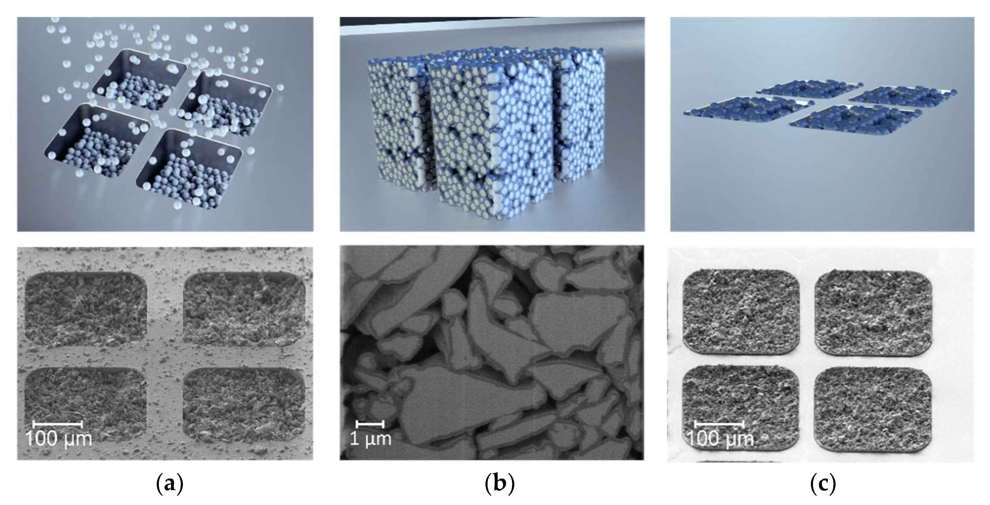
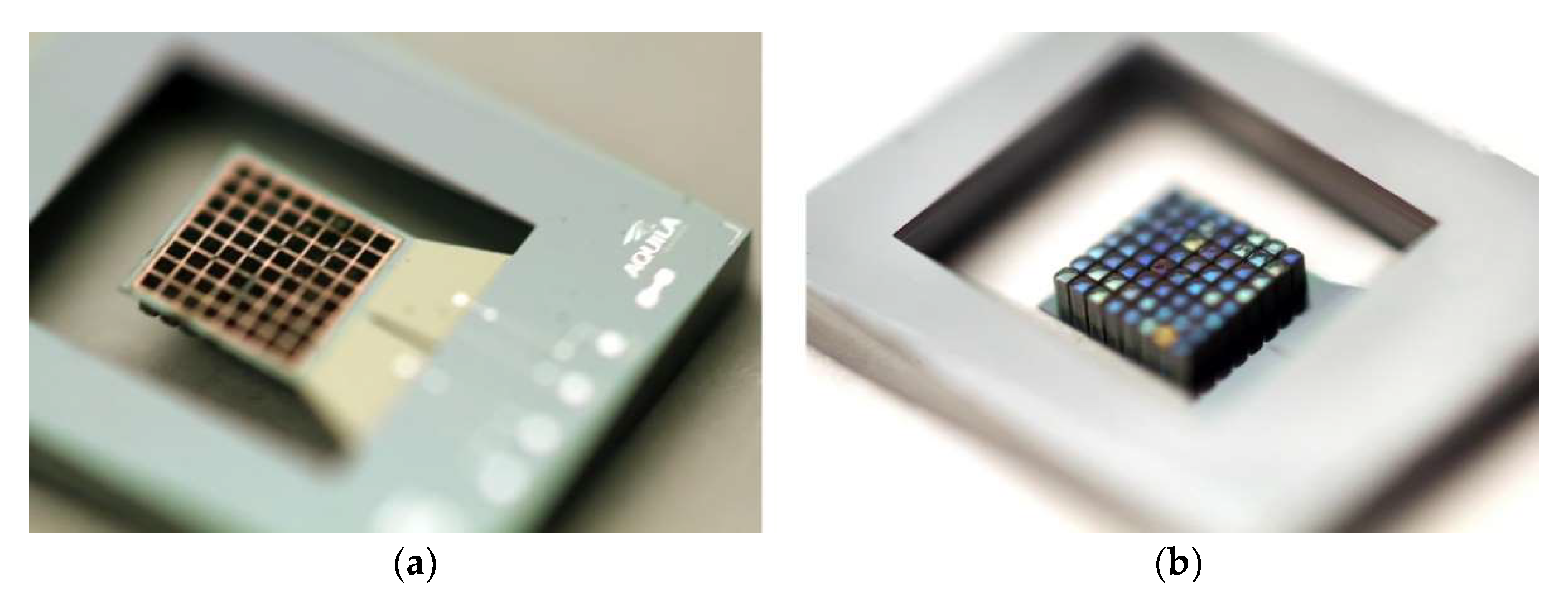
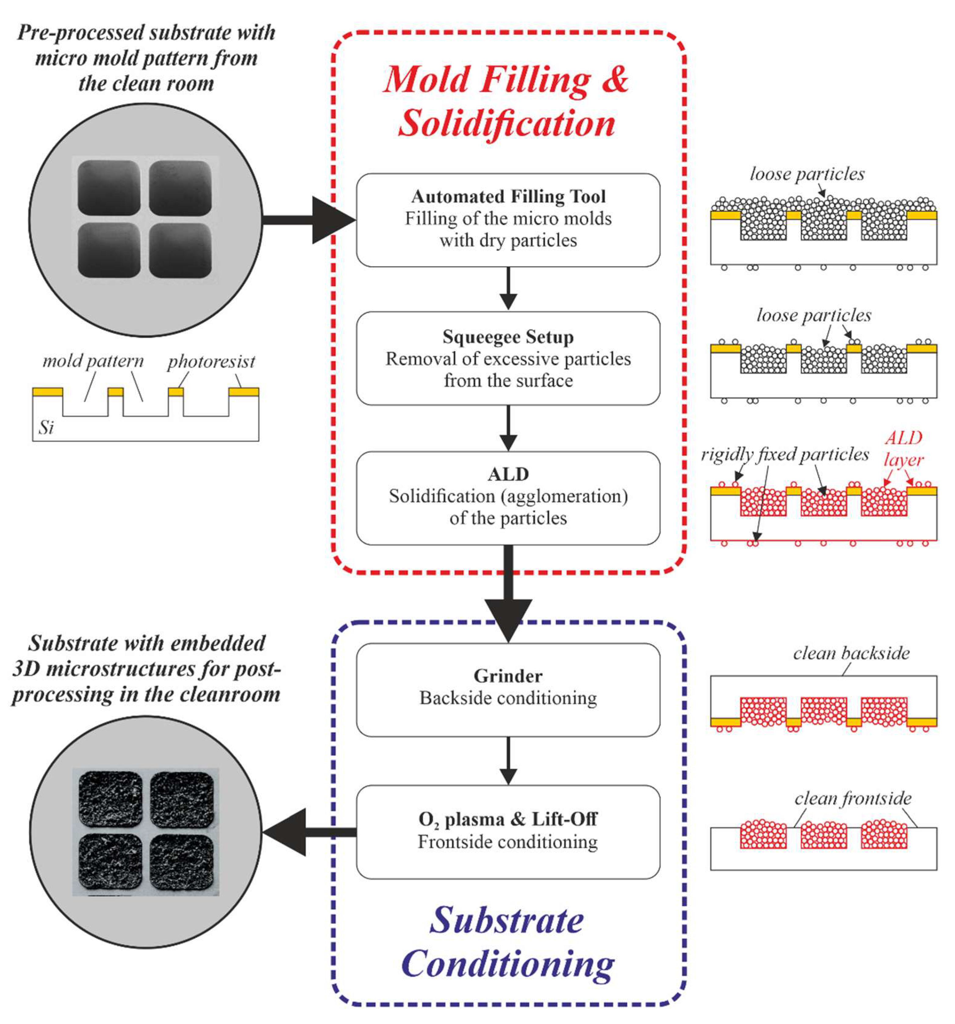
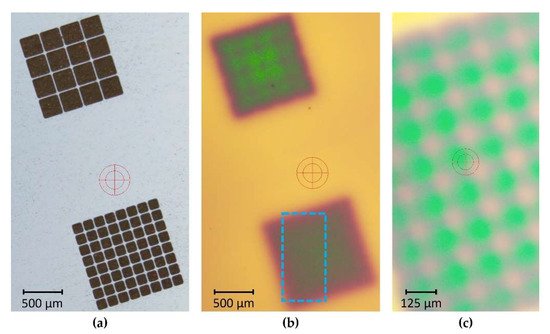
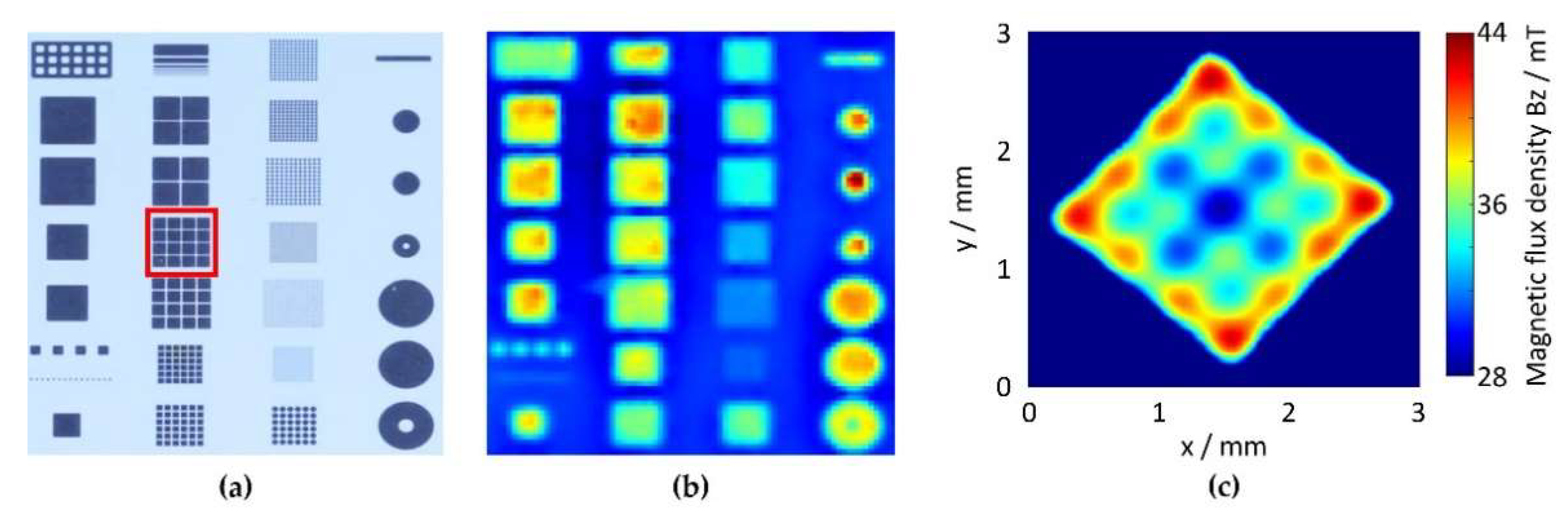
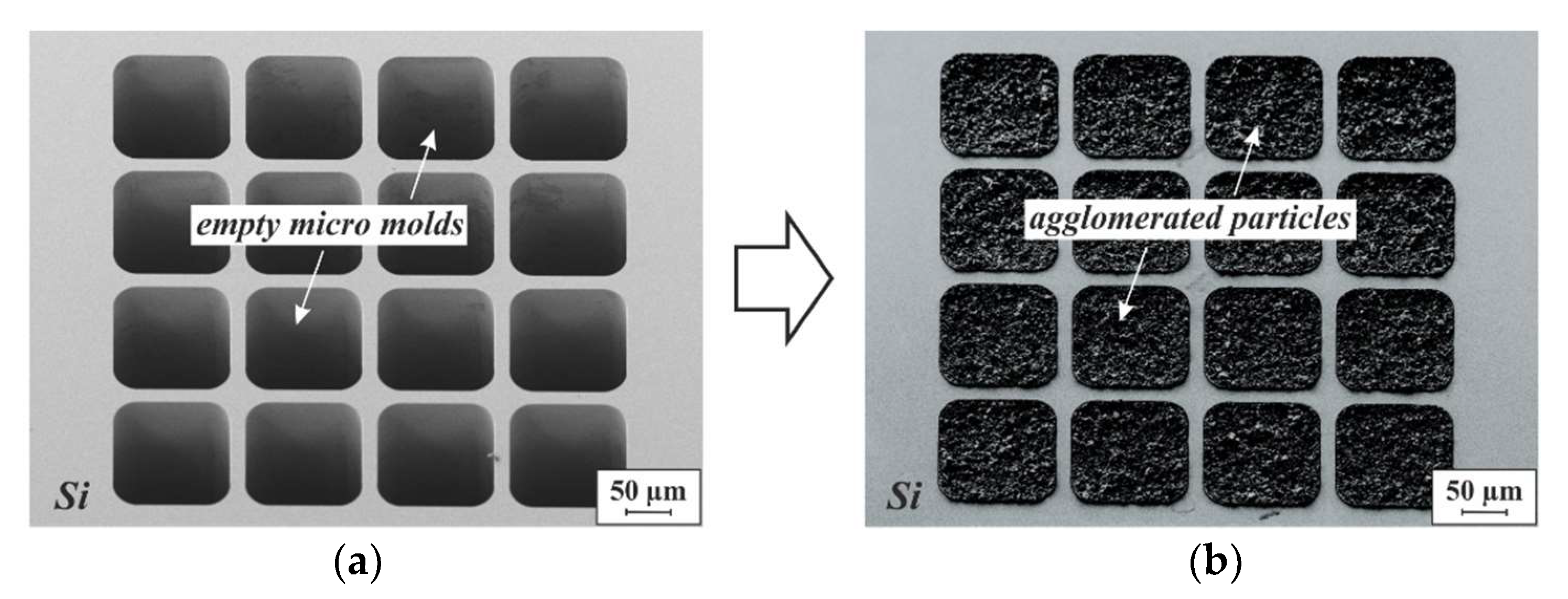
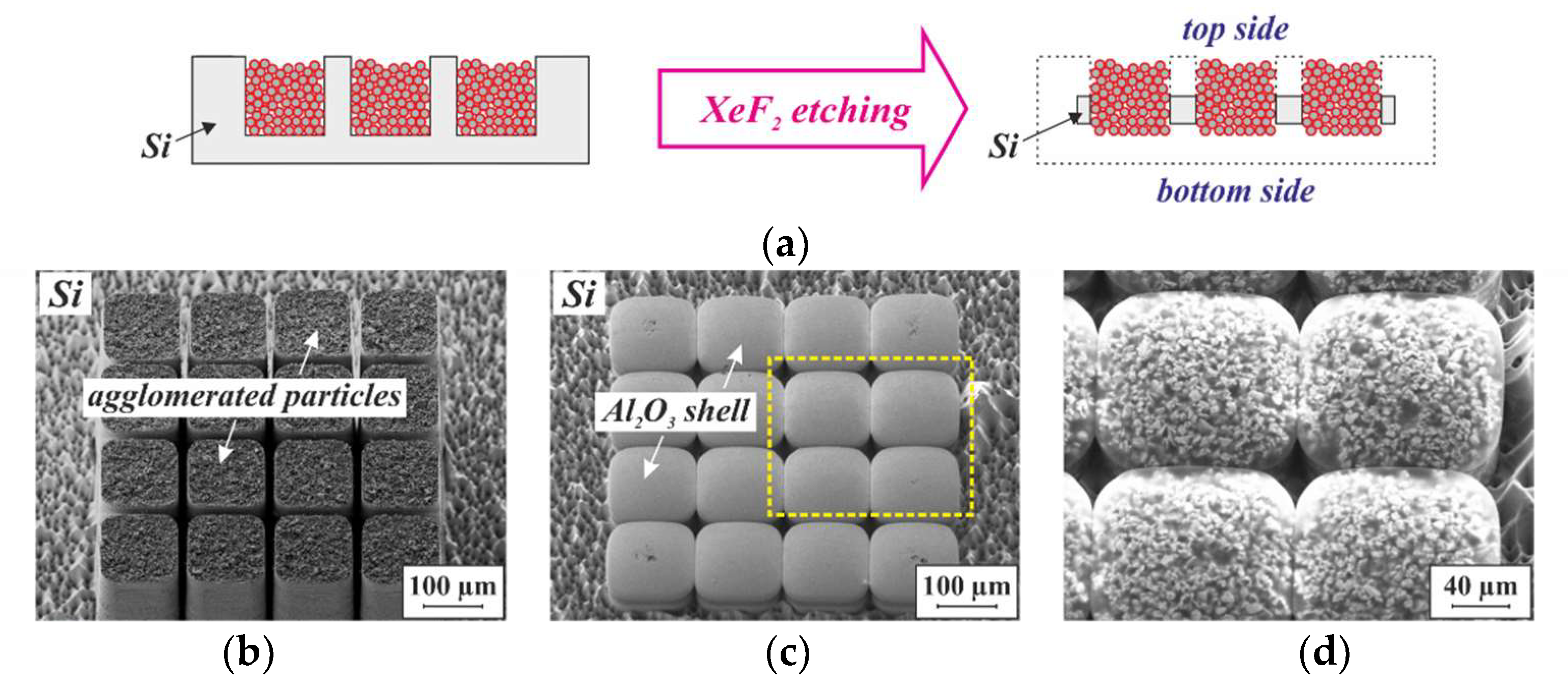
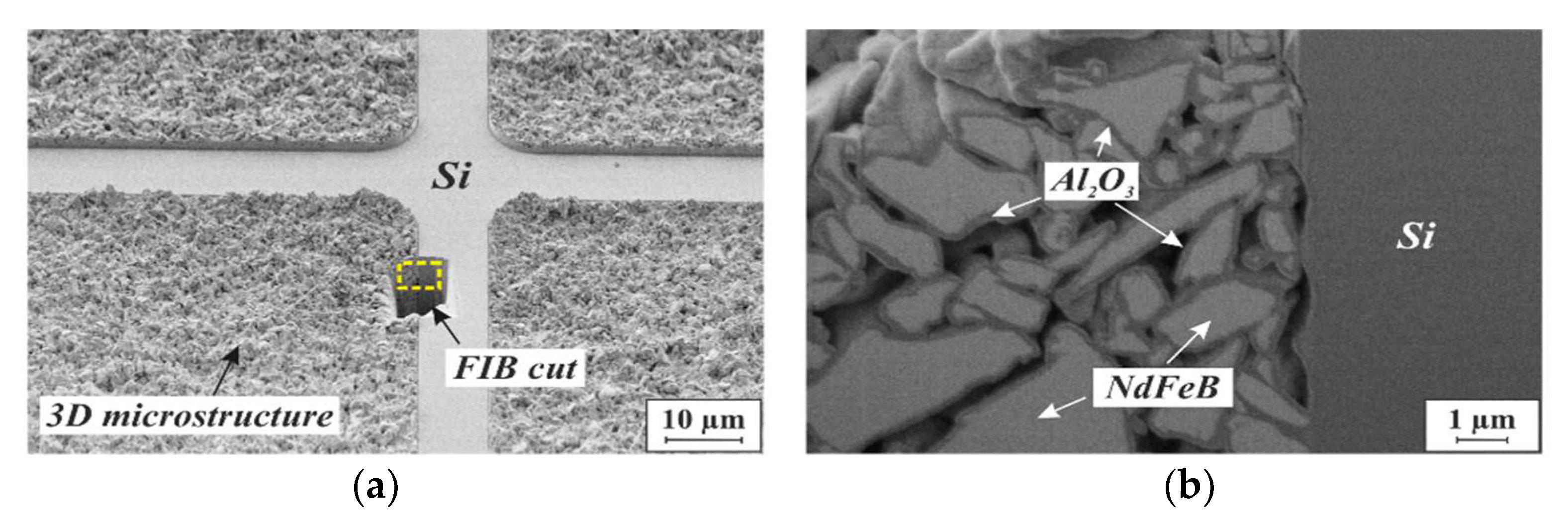
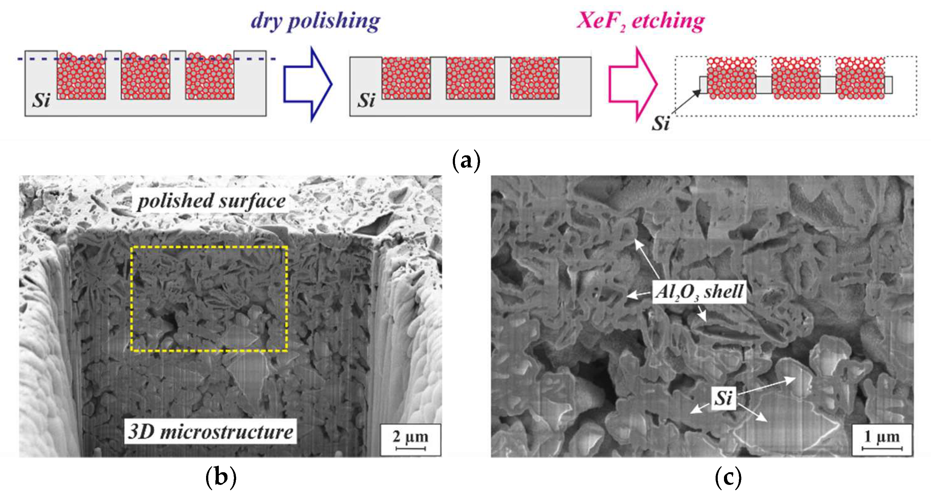
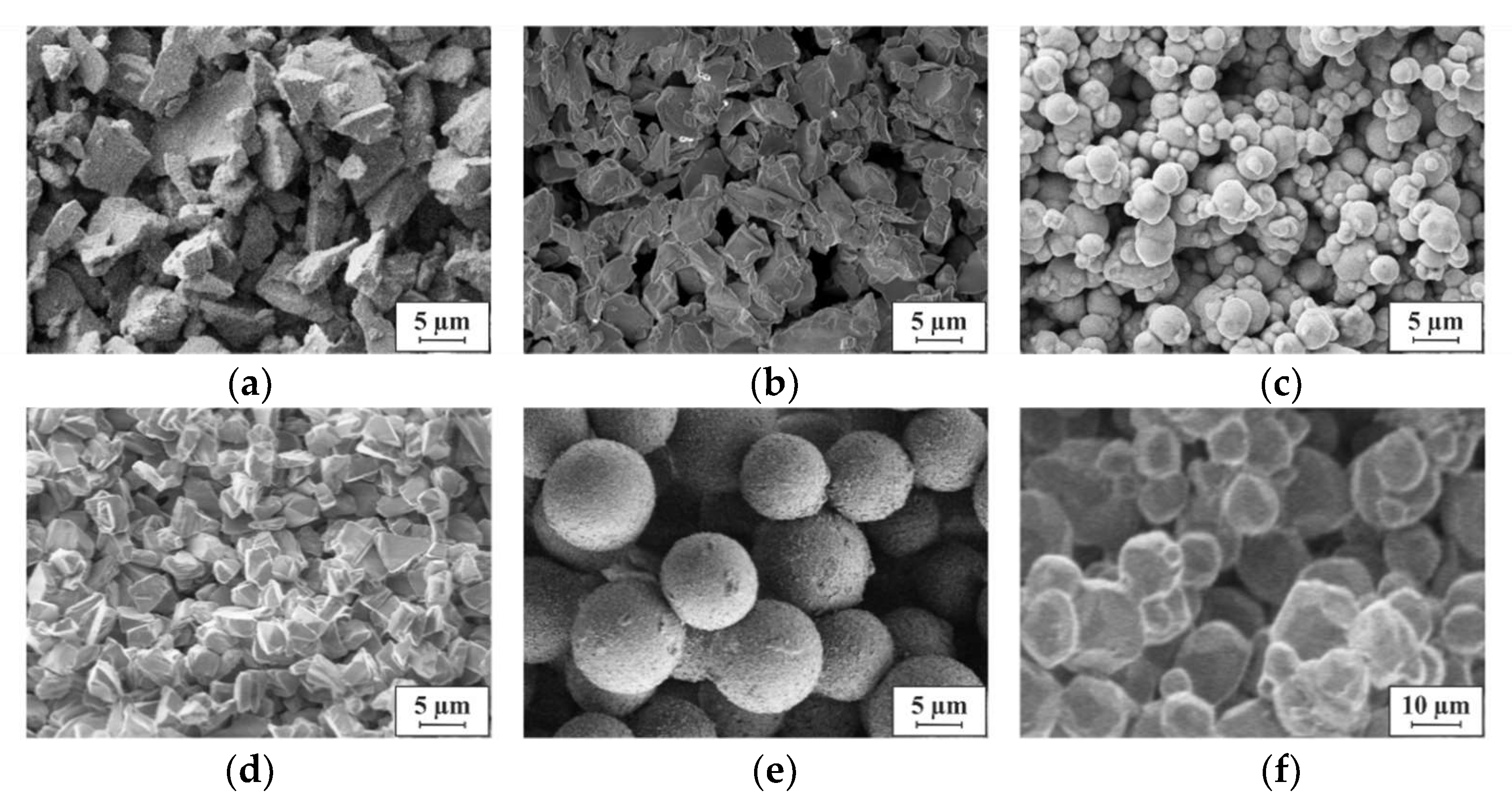
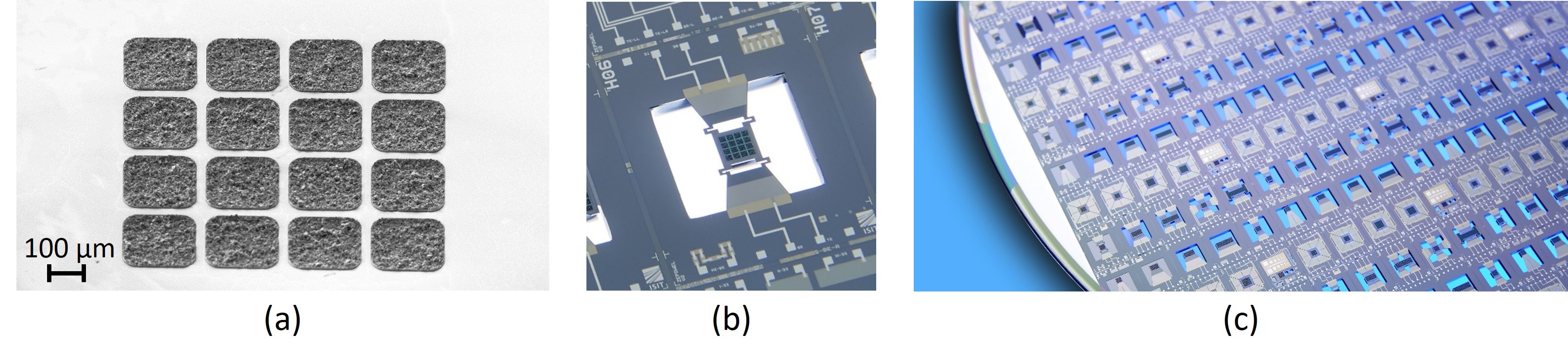 Figure 11. Example of wafer level-integration of NdFeB micromagnets into a MEMS device. (a) NdFeB micropowder solidified by Al2O3 into the silicon device wafer (8 inch / 200 mm). (b) MEMS energy harvesting device with piezoelectric AlN layer (bright grey) and NdFeB micromagnets (black). (c) 200 mm silicon wafer with harvester design variations. All devices contain PowderMEMS NdFeB micromagnets.
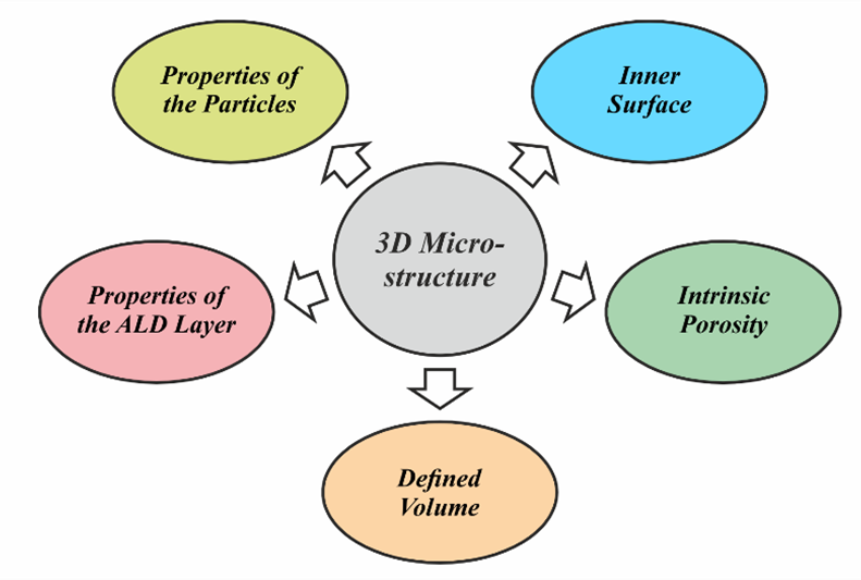 Figure 12. Physical and chemical properties of PowderMEMS 3D microstructures that can be tailored towards specific applications.
