Your browser does not fully support modern features. Please upgrade for a smoother experience.
Submitted Successfully!
 +1 credit
Thank you for your contribution! You can also upload a video entry or images related to this topic.
For video creation, please contact our Academic Video Service.
| Version | Summary | Created by | Modification | Content Size | Created at | Operation |
|---|---|---|---|---|---|---|
| 1 | Francesca Madonini | + 3899 word(s) | 3899 | 2021-06-28 14:15:24 | | | |
| 2 | Conner Chen | Meta information modification | 3899 | 2021-07-01 04:19:07 | | |
Video Upload Options
We provide professional Academic Video Service to translate complex research into visually appealing presentations. Would you like to try it?
Cite
If you have any further questions, please contact Encyclopedia Editorial Office.
Madonini, F. Time-gated Raman spectroscopy. Encyclopedia. Available online: https://encyclopedia.pub/entry/11511 (accessed on 23 July 2026).
Madonini F. Time-gated Raman spectroscopy. Encyclopedia. Available at: https://encyclopedia.pub/entry/11511. Accessed July 23, 2026.
Madonini, Francesca. "Time-gated Raman spectroscopy" Encyclopedia, https://encyclopedia.pub/entry/11511 (accessed July 23, 2026).
Madonini, F. (2021, June 30). Time-gated Raman spectroscopy. In Encyclopedia. https://encyclopedia.pub/entry/11511
Madonini, Francesca. "Time-gated Raman spectroscopy." Encyclopedia. Web. 30 June, 2021.
Copy Citation
Raman spectroscopy is a non-destructive technique which provides information on the physical and chemical structure of a material, based on the interaction of molecule vibrational modes with light. Time-gated Raman spectroscopy is an effective technique to reject the strong fluorescence background that overwhelms Raman signal. It profits from the time scale difference in the two responses: Raman photons are scattered almost instantaneously while fluorescence shows a nanoseconds time constant decay. The combination of short laser pulses with time-gated detectors enables the collection of only those photons synchronous with the pulse, thus rejecting fluorescent ones.
time-resolved Raman spectroscopy
fluorescence suppression
single photon avalanche diode (SPAD)
SPAD array
time gating
single photon counting (SPC)
time-correlated single photon counting (TCSPC)
1. Introduction
1.1. Raman Effect
The Raman effect or combinational scattering of light was discovered in 1928 by Sir C. V. Raman [1] and independently by G. Landsberg and L. Mandelstam [2]. It consists of an inelastic scattering of incident light photons that involves generating new frequencies during the light-matter interaction. These new frequencies are related to the vibrational and rotational modes of the analyte under observation [3]. Since these modes are a unique feature of each single molecule, Raman spectroscopy is a powerful tool to investigate molecular specificity and structure features. One of its greatest advantages is the label-free operation, which avoids any sample preparation and fluorescent marker introduction, making Raman one of the most versatile non-invasive real-time measurement technique.
When the energy of an incident photon is not enough to fill the gap between two electronic energy levels, the molecule can be raised up to a virtual energy level, which is not a real state, but it assumes whatever energy the impinging photon has. Since the virtual state is not a stable energy level, it can be populated only during a transient, followed by a Raman or Rayleigh scattering. In such a case, we talk about non-resonant Raman scattering. With reference to Figure 1, given an incident monochromatic radiation of frequency ωI, if the molecule relaxes emitting a photon at the same frequency ωI, the scattering is of an elastic type, i.e., Rayleigh scattering (Figure 1a). Conversely, when the emitted photon frequency is lower or higher than the original one (i.e., ωI ± ωK), an inelastic (Raman) scattering happens, referred to as Stokes (Figure 1b) and anti-Stokes (Figure 1c) Raman scattering, respectively.
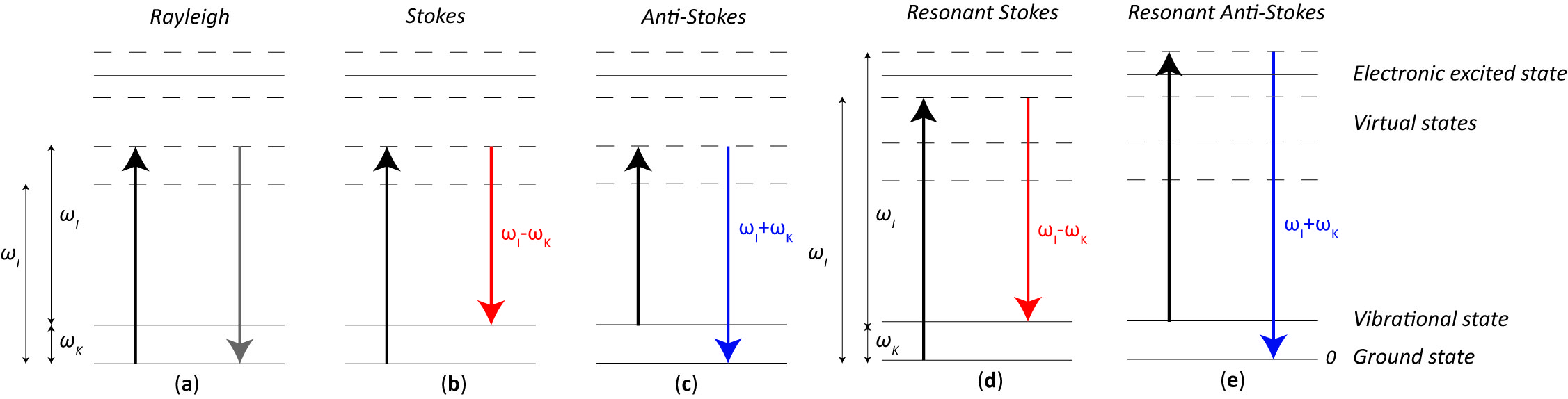
Figure 1. Simplified (a) Rayleigh, (b) non-resonant Stokes Raman, (c) non-resonant Anti-Stokes Raman, (d) resonant Stokes Raman, and (e) resonant anti-Stokes Raman scatterings. The arrows represent the electron jump from one state to the other: in black when the photon energy is absorbed, in grey when a Rayleigh scattering happens, in red and blue when Stokes and anti-Stokes Raman scattering respectively happen.
One should note that ωK is the resonance frequency of the considered vibrational energy level: in a Stokes scattering the molecule relaxes back to an excited vibrational level, whereas an anti-Stokes scattering happens when the molecule was originally on an excited vibrational level and, from a virtual state, it returns to the fundamental one.
Resonant Raman scattering happens when the excitation frequency ωI is very close to the frequency of an electronic transition or, in other words, the virtual state energy level is very close to an electronics excited state, as shown in Figure 1d,e for the Stokes and anti-Stokes case, respectively. This feature makes the Raman process more likely to occur, resulting in a much stronger signal, thus greater sensitivity to detect lower substance concentrations or decrease exposure time.
1.2. Raman Spectra
In spectroscopy, the commonly used unit is the wavenumber ν = 1/λ [cm−1], which allows the definition of the Raman shift Δν [cm−1] as the difference between the incident photon wavenumber νI and the outcoming photon wavenumber νO. The Raman shift includes vibrational information related to each individual molecule, such as its structures and chemical bonds. Compared to Rayleigh scattering, Raman scattering is extremely weak, its intensity being 10−6 smaller than the Rayleigh one for pure liquids and down to 10−12 for powders [4]. As shown in Figure 2, if we refer to only one vibrational mode for sake of simplicity, Raman shifts for Stokes and anti-Stokes process (ΔνS and ΔνAS, respectively) are equal in absolute value, since they are both created from the vibrational resonance frequency ωK and the probe laser frequency ωI. Therefore, also the information contained within Stokes and anti-Stokes sides is the same. However, the intensity of Stokes is far greater than the one associated with anti-Stokes ones. Indeed, their intensity ratio is governed by the sample’s absolute temperature and the energy difference between ground and excited vibrational states. Since the majority of molecules are in the ground state at ambient temperature, the Stokes Raman lines are much more intense. An increase in temperature, which would cause an increase in the population of the excited vibrational states, is not a feasible solution for boosting anti-Stokes intensity because it could compromise the analyte structure.
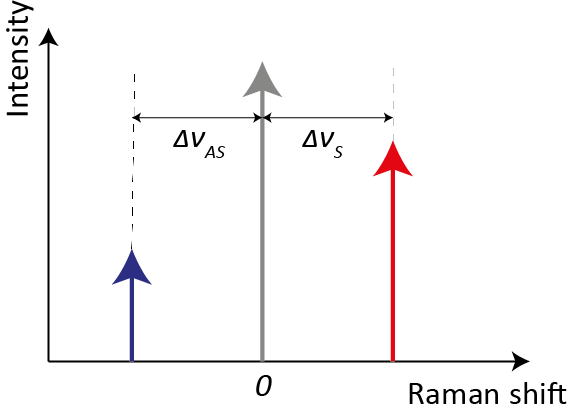
Figure 2. Schematic representation of Raman shifts for Stokes and anti-Stokes processes. The red and blue arrows represent, respectively, the intensities of Stokes and anti-Stokes Raman scattering, whereas the grey arrow represents the Rayleigh scattering (not in scale).
Ambient light affects the quality of Raman signal, thus common straightforward solutions are to perform Raman measurements in a dark environment or place the sample in a stray-light sealed enclosure. A complete enclosure is difficult to be achieved with on-site outdoor measurements [5]. Rayleigh scattering also constitutes a strong background light overwhelming Raman bands due to its higher intensity; therefore, it must be rejected, for example, through an optical notch filter in applications exploiting both Stokes and anti-Stokes spectra [6]. Since filters with strong in-band attenuation and sharp edges should be employed in order not to compromise other spectral components, in conventional Raman spectroscopy, it is simpler to use a long-pass filter, cutting out also the anti-Stokes side (carrying the same information content of the Stokes one) while saving the higher intensity Stokes one.
Eventually, the Stokes Raman band is also overwhelmed by fluorescence, due to electrons excited to a higher electronic energy level that, after a relaxation time, return to their ground state through the emission of photons at a longer wavelength [7]. Fluorescence happens when the absorbed photon has enough energy to promote transitions between two allowed energy levels. Therefore, it is most likely to happen in resonant Raman spectroscopy, with source frequencies near to the ones corresponding to molecule electronic transitions. Due to its higher intensity, fluorescence signal typically overshadows Raman scattering, and it cannot be filtered without also eliminating Stokes band, since they are both located at longer wavelengths (i.e., lower energy).
1.3. Raman Spectrometer System
Figure 3 shows the five fundamental components of a dispersive Raman spectrometer: a laser excitation source; a light collection system for focusing light onto the sample and collecting the scattered light; an optical filter to cut out Rayleigh components; a diffraction element (e.g., a diffraction grating) to disperse the light into its spectral components; and a detector. The diffraction element selection is key for the final spectral resolution: full-scale range (FSR) and resolution depend on the spatial wavelength spread of the grating [8].
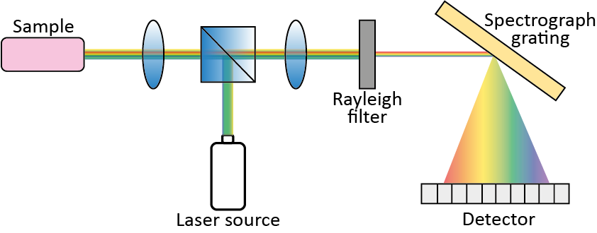
Figure 3. Typical components of a Raman spectrometer.
The laser frequency selection strictly relates to the desired fluorescent background rejection, as well as to the Raman signal intensity. In fact, Raman bands’ intensity is proportional to the inverse 4th power of wavelength [9]; therefore, shorter wavelength lasers give rise to stronger Raman intensities. However, the higher the photon energy, the higher the chance of exciting specific sets of fluorophores, which may contribute to fluorescence. Since both Raman and fluorescence increase at shorter stimulation wavelengths, a trade-off is needed. Laser wavelengths in the near Infra-Red (NIR) range (typically 785–1064 nm), where fluorescence is no longer a problem, often make the Raman intensity too low and thus the Raman-to-fluorescence signal disadvantageous. Furthermore, silicon detectors, which are less expensive than other III-V materials and can be integrated together with electronics in single-chip detection systems, have a low sensitivity in the NIR [10]. Using a UV (<400 nm) laser wavelength has a clear advantage in terms of Raman efficiency, but fluorescence is enhanced too. For deep UV (<260 nm), fluorescence stays in the visible range, thus not overlapping with Raman spectra [11]; however, optics, lasers, detectors, and high-resolution spectrographs are difficult to be designed and the related high photon energy risks to damage the sample. Furthermore, UV light would be absorbed just in a very thin surface layer, thus not allowing deep sample analysis. Eventually, techniques to eliminate or at least reduce fluorescence impact must be implemented.
Photobleaching permanently kills the fluorophore ability to fluoresce, due to photon-induced chemical damage and covalent bond modification. Such modification can be obtained by illuminating the specimen with the excitation laser over an extended period of time. Besides being slow, this process induces chemical and physical changes that cannot be tolerated by some materials (e.g., living cells). Thus, photobleaching is not a suitable answer to reduce fluorescence [12].
Eventually, different possible techniques to improve Raman signal compared to fluorescence have been reviewed in [13], where they are classified into time-domain, frequency-domain, wavelength-domain, and computational methods.
Among time-domain methods, which exploit the different time scales of Raman and fluorescence processes, an effective solution is the exploitation of Time-Gated (TG) detectors. Figure 4 shows a schematic time profile of a Raman band with a fluorescence background following the laser pulse. The fluorescence photon is emitted with an average characteristic delay, while Raman scattering is theoretically instantaneous, even if significant temporal broadening (even hundreds of picoseconds) can be measured from thick scattering samples [14]. The typical Raman time scales are in the sub-picoseconds to picoseconds range, whereas fluorescence ones are in the hundreds of picoseconds to nanoseconds range [15]. The limit in decreasing the laser pulse width to get an even shorter Raman signal is represented by the minimum laser power requested for Raman scattering, whose intensity is indeed proportional to the laser power. Reducing the laser pulse width requests increasing the laser peak power, which could lead to sample damage or alteration [16]. Using a TG photodetector, it is possible to record only the part of the emission pulse related to the Raman effect, while rejecting the fluorescence tail. Instead, the residual fluorescence (RFL) already emitted during the pulse, thus overlapping the Raman signal, cannot be rejected. Various algorithms can be exploited in post-processing to enhance the acquired signal accuracy, based on the identification of Raman spectra peaks, distinguishable only after TG operation [17][18][19][20].
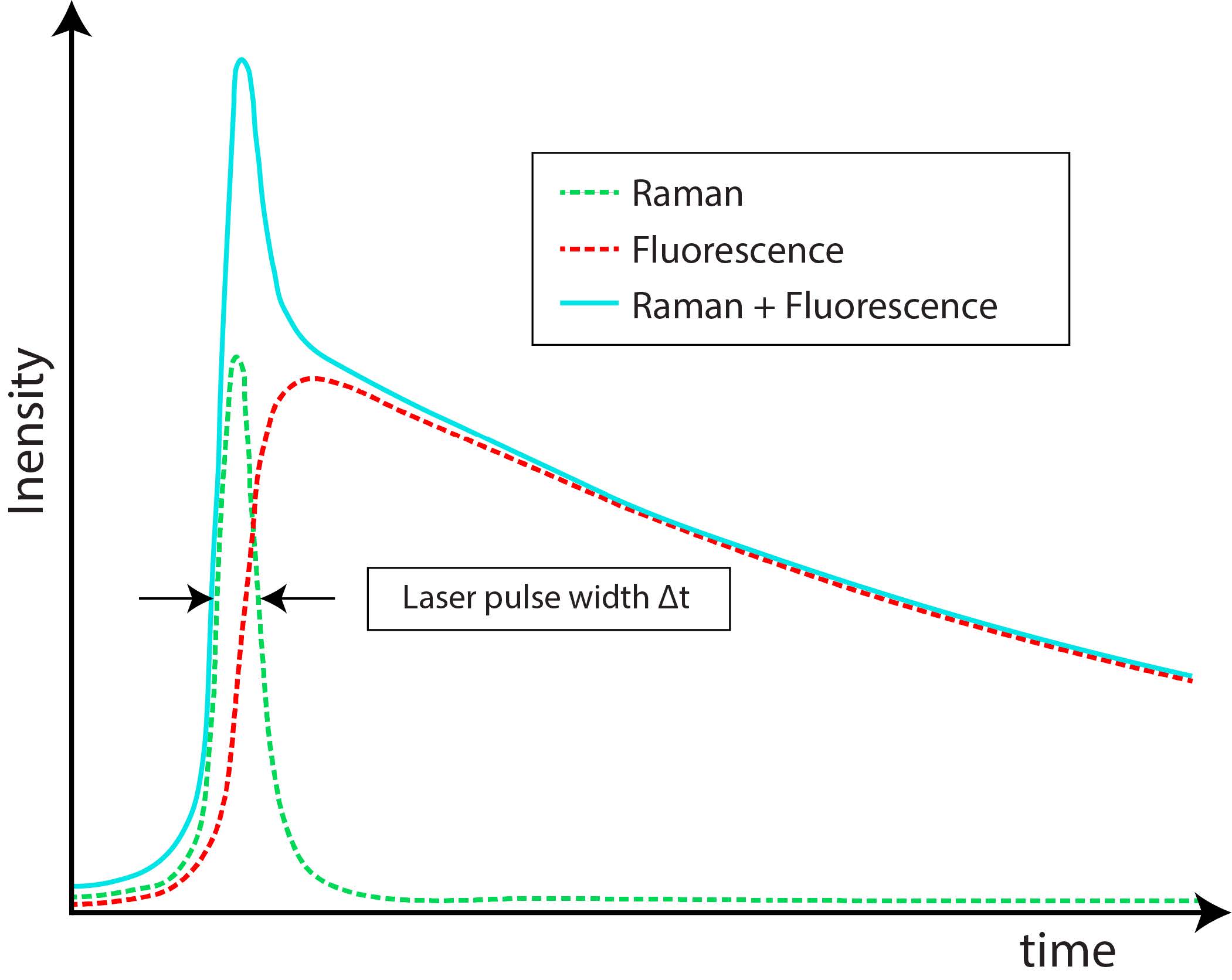
Figure 4. Raman and fluorescence signal time profiles [15]. Note that Raman intensity can be even much lower than the fluorescence one.
As highlighted in [21], a typical TG Raman setup includes a pulsed laser source with repetition rate in MHz range, picosecond-range pulse width, and suitable pulse energy. The latter must be enough to excite the sample spot, and just a minor fraction be used to synchronize the detector through a delay generator, matching the detection sequence delay, as shown in Figure 5.
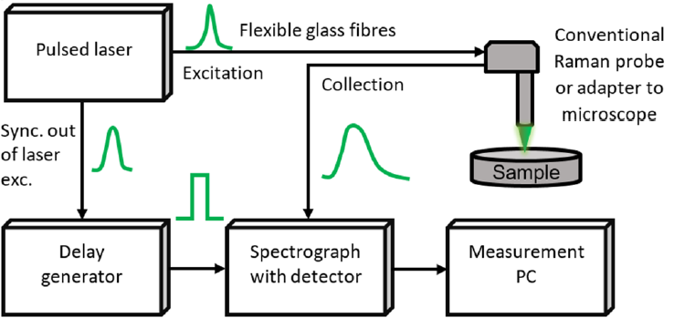
Figure 5. General block diagram of TG spectrometer, showing that the pulsed laser, through a delay generator, is used to trigger (i.e., to gate) the detector [21].
2. Detectors
Photomultiplier tubes (PMTs) were the first detectors employed in sensitive Raman technique measurements [22]. They are based on photoelectric effect and secondary emission, and they are sensitive in the UV, visible, and NIR ranges of the electromagnetic spectrum. Nevertheless, they show several limitations. First, they are single-point detectors, meaning that they force each single spectral component to be scanned separately (i.e., the grating has to be moved and a new measurement acquired). Therefore, as the required spectral resolution increases, the acquisition time rises proportionally, and all experimental parameters have to remain constant during the scan. Furthermore, PMT devices cannot be electronically time-gated. Microchannel-plate photomultipliers (MCP-PMTs) solve spatial resolution issues since they include many channels. However, like PMTs they are not suitable for integration, and their photocathode can be damaged by prolonged exposure to light [23].
Charge-coupled devices (CCDs) have been the new generation of multichannel detection systems for Raman spectroscopy [24]. They are arrays of detectors storing a quantity of charge (proportional to the incoming radiation), which is then transferred from each element to the nearby one for readout [25]. By being an array, the whole spectrum can be acquired at once, with a clear advantage in terms of acquisition time. They ensure high sensitivity up to NIR [26], low noise related to dark current, even if they suffer from slow readout speed. Several research groups trigger CCDs by using Optical Kerr-gating [27], acting like a light shutter in front of the spectrometer entrance, or streak cameras [28]. However, such setups limit system portability due to the required bulky equipment. Intensified charge-coupled devices (ICCDs) provide a much more advanced solution for electronic gating (through the photocathode biasing) [29]. As a notable example of Raman measurements, ref. [30] reached a high fluorescence suppression with a state-of-the-art ICCD camera designed for fast gating at a repetition rate up to 110 MHz and a gate width shorter than 200 ps, time jitter lower than 20 ps, photocathode sensitivity in 400–900 nm range across 1376 × 1040 pixels, 10 frames/s readout, and 65% quantum efficiency. ICCDs main drawbacks are high power consumption (due to the high-voltage devices) often requiring Peltier cooling, photo-degradation (similar to PMTs), size, and cost. ICCD low frame rate is instead balanced by the ability to perform several counts per laser pulse, like any linear detector. Features, performances, and drawbacks of Kerr-gating and ICCDs are summarized in [31].
Single photon avalanche diodes (SPADs) are solid-state sensors based on reverse-biased p-n junctions where the electron-hole pair generated by the absorption of a single photon ignites an avalanche current build-up, easily sensed by the front-end electronics, which outputs a digital pulse. By switching the reverse voltage from slightly below to above the breakdown voltage and vice versa, SPADs can be easily time-gated on and off. CMOS SPADs are Si-made, and their major advantage is the easy integration with microelectronics since they can be made within the same fabrication processing. Regarding Raman spectroscopy, Si-SPAD main drawback is their low sensitivity in the NIR range, due to the relatively thin depletion layer of CMOS SPADs compared to thick-junction ones [32][33][34]. InGaAs/InP [35][36] or Ge [37][38], whose energy gaps are much lower than the Si one, are used to detect NIR photons, however they cannot be monolithically integrated with electronics and need to be cooled for reducing the intrinsic noise.
First demonstrations of TG Raman spectroscopy employing a single SPAD moved by a step motor with small steps to cover the full Raman shift range were reported in [39][40]. A strong fluorescence suppression was demonstrated with 300 ps time-gate windows. Then, the potential large-scale manufacturability of CMOS SPADs soon drove the development of SPAD arrays for TG Raman. Indeed, SPADs digital-like output pulses allow easy on-chip digital processing also for many-pixels arrays. In fact, SPAD arrays fulfil the desired spatial resolution, besides high sensitivity, limited power dissipation, no need for cooling over a wide temperature range, sub-ns time gating, and large-scale miniaturized chip formats.
3. SPAD Array Requirements for TG Raman Spectroscopy
An array detector provides many pixels, laid out in a linear or two-dimensional format. Typically, there is no need for an array with a 1:1 (squared) aspect ratio in dispersive Raman spectroscopy, since the diffraction element spreads Raman wavelengths across a spectrum of lines. Hence, a linear array simplifies the whole system architecture because, by confining all detectors in a defined area, the electronics can be implemented aside, thus not impairing the Fill-Factor (FF), when considering standard planar technologies. FF is a fundamental figure of merit related to the SPAD active area, the pixel geometry, and the pixel array layout, and it is defined as the ratio between the detection active area and the total area illuminated by Raman light. Figure 6a,b underline the difference between a classical architecture with in-pixel electronic, usually employed in near 1:1 aspect-ratio arrays, and out-of-pixel electronics, more suitable for linear arrays. Out-of-pixel electronics also allows achieving a significantly smaller pixel pitch, thus increasing spatial resolution. As shown in Figure 6c, in a linear Raman array, the required number of pixels in the longer dimension, i.e., number of columns, depends on the number of spectral lines to be discriminated (i.e., wavenumber) and on the desired spectral resolution. These two parameters are specific for each Raman application and sample and depend on the optical system. The latter also defines the desired number of SPAD rows, that should match the transversal photon distribution given by the optical grating. In other words, more SPADs can be arranged in the same column pixels to increase the detected signal without losing in spectral resolution.
Figure 6. Example of (a) in-pixel and (b) out-of-pixel electronics for generic linear arrays, and (c) column pixels (associated to Raman lines) with out-of-pixel electronics for Raman linear arrays.
In-pixel electronics is no more an FF limitation when considering a 3D-stacked approach, where a top-tier includes SPADs fabricated in an optimized CMOS Image Sensor (CIS) process, while all processing electronics is implemented in a bottom-tier chip in a more scaled-down technology [41].
Discussing spatial resolution, the minimum distance between adjacent SPADs benefits from advanced isolation techniques, such as deep trench isolation (DTI) [42], which guarantees voltage isolation, parasitic reduction, and crosstalk minimization with narrow clearance among SPADs. Eventually, detector spatial resolution and pixel pitch directly translate into spectral resolution of Raman shifts.
Obviously, besides FF, high photon detection probability (PDP), defined as the ratio between detected and incident photons within the active area, is a key parameter to maximize photon detection. PDP is intrinsically related to the SPAD; FF depends on the array layout; the product of the two gives the overall photon detection efficiency (PDE). In Raman spectroscopy, the relative position of Raman bands with respect to the excitation frequency is independent of the excitation frequency itself. Therefore, the designer should choose an excitation frequency where the PDP is maximum. For further improving FF, hence PDP, a microlenses array (MLA) can be employed to precisely focus light onto the active areas.
The most relevant SPAD noise contribution is given by dark-count-rate (DCR) events, i.e., intrinsic avalanche generation rate of the detector in absence of illumination. A good quality fabrication technology, reducing lattice defects and minimizing generation-recombination centers [43], is essential to improve detector noise. In large-size arrays, it is common to find some “hot pixels”, which are pixels showing a DCR much higher than the median DCR of the array, usually related to local defects. Since their presence negatively impacts the imager performance, the array should embed a way to selectively disable them during an initial configuration. However, in TG SPAD arrays, the gate on/off duty-cycle helps decreasing the probability of detecting dark counts [40].
Combining a picosecond excitation pulse with a sub-nanosecond TG allows an effective main rejection of the broad unwelcome fluorescence. The rejection degree is roughly proportional to the ratio between fluorescence time constant and gate width [44], which should ideally match the laser pulse width to maximize the collection of Raman photons scattered during the pulse, but reject the delayed fluorescence. Indeed, different gate widths and positions determine signal-to-noise ratio (SNR) changes according to:

In this regard, fast and precise detector gating capability is needed. Two different approaches are possible: “hard-gating” and “soft-gating”. In “hard-gating”, SPADs are disabled outside the gate window, by biasing them below the breakdown voltage through additional transistors in their front-end circuitry, that therefore should provide both a fast activation and deactivation of the SPAD [46]. In “soft-gating”, SPADs are not actively disabled, but the front-end’s digital output is masked to the subsequent processing electronics or, in other words, the counting or timing logic is disabled outside the gate window. In this case, rising and falling edges of the activation signal are only limited by the speed of the logic gates. In both approaches, the electronic blocks generating gate signals should be carefully designed to minimize time skews, which cause gate shifts and gate-width variations across array positions (i.e., wavelength points), becoming even larger when the number of SPADs in the array increases. This detrimental effect would give a different photon count at different spectral points even if the signal intensity remains the same [47]. To avoid distortion in the detected Raman spectrum, it is important that all pixels get activated in the same time interval, perfectly synchronized with Raman signal. [47] also computes signal-to-RMS-distortion ratio to define the quality of the spectra. Conversely, when fluorescence is rejected by post-processing time-to-digital converter (TDC) data, slower and less precise gate signals are needed if TDC resolution is enough to distinguish Raman and fluorescent photons. Also in this case, time skews related to TDC signals (e.g., delay lines and clocks) should be minimized, since they could affect the conversion precision. However, the TDC-based approach has the disadvantages of requiring a TDC per pixel, storing only one photon per pixel per time-frame, and slowing down the readout phase.
With high-performance timing electronics, the bottleneck could be set by the intrinsic SPAD performance, namely time-jitter and exponentially decaying tail [48]. Time-jitter refers to the statistical distribution of delays from the actual photon arrival to the actual detection time. Instead, the exponential tail is given by photons absorbed in the neutral region (instead of the high electric field depleted region of the SPAD junction), able to trigger avalanches after a not negligible delay from the actual photon absorption: it depends both on light wavelength and SPAD cross-section. Moreover, high excess bias is beneficial because it increases the avalanche current, which can be more precisely detected by the sensing electronics [49]. The obvious effect of these non-idealities is the time spreading of the SPAD ignition, thus the need of expanding the gate duration to match both laser width and SPAD jitter, thus increasing the detection of fluorescent photons present within the time gate and deteriorate the SNR according to (1).
When a photon is absorbed and the avalanche is triggered, the SPAD sensing and quenching circuit stops the current, preventing power dissipation, and restores the SPAD initial conditions after a given hold-off time [33]. The latter is necessary to release the charge trapped inside the junction, if any, that could retrigger the SPAD if brought above breakdown too soon, thus giving false events correlated to the primary ignition, called afterpulses [50]. Hold-off times in the 20–50 ns range are enough to limit afterpulsing to less than 1% in Si SPADs.
The gating frequency should be sufficiently high to repeat the laser excitation to collect a sufficient number of Raman photons within a reasonably short measurement time. At the same time, the repetition rate should be reduced to limit the overall system power consumption. The latter, indeed, is strictly related to the risk of overheating and consequently DCR increasing. If the chip temperature is kept limited without the need of a cooling system, the portability and compactness of the complete system is not compromised. Furthermore, TG inherently leads to significant dynamic power consumption, above all in the case of very fast on/off transitions applied to detectors with large capacitive loading. Therefore, particular care should be given to minimize cross-conduction currents (e.g., due to non-perfect synchronism between the signals that turn on and off the SPADs) and static power consumption due to leakage currents.
Finally, the array readout architecture plays an important role in achieving high frame-rate, hence short overall measurement time. For example, a double-buffered readout allows to perform a new acquisition while the previous data is being transferred to the on-chip electronics or to off-chip processing, virtually eliminating the typical dead time of global shutter.
References
- Raman, C.V.; Krishnan, K.S. A New Type of Secondary Radiation. Nature 1928, 121, 501–502.
- Mandelstam, G.; Landsberg, L. Eine neue Erscheinung bei der Lichtzerstreuung in Krystallen. Naturwissenschaften 1928, 16, 557–558.
- Gordon, R.G.; Klemperer, W.; Steinfeld, J.I. Vibrational and Rotational Relaxation. Annu. Rev. Phys. Chem. 1968, 19, 215–250.
- Zhu, X.; Xu, T.; Lin, Q.; Duan, Y. Technical development of raman spectroscopy: From instrumental to advanced combined technologies. Appl. Spectrosc. Rev. 2014, 49, 64–82.
- Blacksberg, J.; Alerstam, E.; Maruyama, Y.; Cochrane, C.J.; Rossman, G.R. Miniaturized time-resolved Raman spectrometer for planetary science based on a fast single photon avalanche diode detector array. Appl. Opt. 2016, 55, 739.
- Kauffmann, T.H.; Kokanyan, N.; Fontana, M.D. Use of Stokes and anti-Stokes Raman scattering for new applications. J. Raman Spectrosc. 2019, 50, 418–424.
- Lakowicz, J. (Ed.) Principles of Fluorescence Spectroscopy, 3rd ed.; Springer: Boston, MA, USA, 1983.
- Grabarnik, S.; Emadi, A.; Sokolova, E.; Vdovin, G.; Wolffenbuttel, R.F. Optimal implementation of a microspectrometer based on a single flat diffraction grating. Appl. Opt. 2008, 47, 2082–2090.
- Long, D.A. The Raman Effect: A Unified Treatment of the Theory of Raman Scattering by Molecules; John Wiley & Sons, Ltd.: Chichester, West Sussex, UK, 2002.
- Villa, F.; Bronzi, D.; Zou, Y.; Scarcella, C.; Boso, G.; Tisa, S.; Tosi, A.; Zappa, F.; Durini, D.; Weyers, S.; et al. CMOS SPADs with up to 500 μm diameter and 55% detection efficiency at 420 nm. J. Mod. Opt. 2014, 61, 102–115.
- Abbey, W.J.; Bhartia, R.; Beegle, L.W.; De Flores, L.; Paez, V.; Sijapati, K.; Sijapati, S.; Williford, K.; Tuite, M.; Hug, W.; et al. Deep UV Raman spectroscopy for planetary exploration: The search for in situ organics. Icarus 2017, 290, 201–214.
- Macdonald, A.M.; Wyeth, P. On the use of photobleaching to reduce fluorescence background in Raman spectroscopy to improve the reliability of pigment identification on painted textiles. J. Raman Spectrosc. 2006, 37, 830–835.
- Wei, D.; Chen, S.; Liu, Q. Review of Fluorescence Suppression Techniques in Raman Spectroscopy. Appl. Spectrosc. Rev. 2015, 50, 387–406.
- Hooijschuur, J.-H.; Iping Petterson, I.E.; Davies, G.R.; Gooijer, C.; Ariese, F. Time resolved Raman spectroscopy for depth analysis of multi-layered mineral samples. J. Raman Spectrosc. 2013, 44, 1540–1547.
- Rojalin, T.; Kurki, L.; Laaksonen, T.; Viitala, T.; Kostamovaara, J.; Gordon, K.C.; Galvis, L.; Wachsmann-Hogiu, S.; Strachan, C.J.; Yliperttula, M. Fluorescence-suppressed time-resolved Raman spectroscopy of pharmaceuticals using complementary metal-oxide semiconductor (CMOS) single-photon avalanche diode (SPAD) detector. Anal. Bioanal. Chem. 2016, 408, 761–774.
- Oracz, J.; Westphal, V.; Radzewicz, C.; Sahl, S.J.; Hell, S.W. Photobleaching in STED nanoscopy and its dependence on the photon flux applied for reversible silencing of the fluorophore. Sci. Rep. 2017, 7, 11354.
- Angel, S.M.; DeArmond, M.K.; Hanck, K.W.; Wertz, D.W. Computer-controlled instrument for the recovery of a resonance Raman spectrum in the presence of strong luminescence. Anal. Chem. 1984, 56, 3000–3001.
- Zhao, J.; Lui, H.; McLean, D.I.; Zeng, H. Automated Autofluorescence Background Subtraction Algorithm for Biomedical Raman Spectroscopy. Appl. Spectrosc. 2007, 61, 1225–1232.
- Zhang, Z.-M.; Chen, S.; Liang, Y.-Z.; Liu, Z.-X.; Zhang, Q.-M.; Ding, L.-X.; Ye, F.; Zhou, H. An intelligent background-correction algorithm for highly fluorescent samples in Raman spectroscopy. J. Raman Spectrosc. 2010, 41, 659–669.
- Cadusch, P.J.; Hlaing, M.M.; Wade, S.A.; McArthur, S.L.; Stoddart, P.R. Improved methods for fluorescence background subtraction from Raman spectra. J. Raman Spectrosc. 2013, 44, 1587–1595.
- Kögler, M.; Heilala, B. Time-gated Raman spectroscopy—A review. Meas. Sci. Technol. 2020, 32, 012002.
- Rank, D.H.; Pfister, R.J.; Coleman, P.D. Photoelectric Detection and Intensity Measurement in Raman Spectra. J. Opt. Soc. Am. 1942, 32, 390–396.
- Matsuoka, K.; Hirose, S.; Iijima, T.; Inami, K.; Kato, Y.; Kobayashi, K.; Maeda, Y.; Omori, R.; Suzuki, K. Extension of the MCP-PMT lifetime. Nucl. Instrum. Methods Phys. Res. Sect. A Accel. Spectrometers Detect. Assoc. Equip. 2017, 876, 93–95.
- Murray, C.A.; Dierker, S.B. Use of an unintensified charge-coupled device detector for low-light-level Raman spectroscopy. J. Opt. Soc. Am. A 1986, 3, 2151–2159.
- Burke, B.; Jorden, P.; Vu, P. CCD Technology. Exp. Astron. 2005, 19, 69–102.
- Baraga, J.J.; Feld, M.S.; Rava, R.P. Rapid Near-Infrared Raman Spectroscopy of Human Tissue with a Spectrograph and CCD Detector. Appl. Spectrosc. 1992, 46, 187–190.
- Matousek, P.; Towrie, M.; Ma, C.; Kwok, W.M.; Phillips, D.; Toner, W.T.; Parker, A.W. Fluorescence suppression in resonance Raman spectroscopy using a high-performance picosecond Kerr gate. J. Raman Spectrosc. 2001, 32, 983–988.
- Tahara, T.; Hamaguchi, H.-O. Picosecond Raman Spectroscopy Using a Streak Camera. Appl. Spectrosc. 1993, 47, 391–398.
- Cester, L.; Lyons, A.; Braidotti, M.C.; Faccio, D. Time-of-Flight Imaging at 10 ps Resolution with an ICCD Camera. Sensors 2019, 19, 180.
- Martyshkin, D.V.; Ahuja, R.C.; Kudriavtsev, A.; Mirov, S.B. Effective suppression of fluorescence light in Raman measurements using ultrafast time gated charge coupled device camera. Rev. Sci. Instrum. 2004, 75, 630–635.
- Chiuri, A.; Angelini, F. Fast gating for Raman spectroscopy. Sensors 2021, 21.
- Gulinatti, A.; Ceccarelli, F.; Ghioni, M.; Rech, I. Custom silicon technology for SPAD-arrays with red-enhanced sensitivity and low timing jitter. Opt. Express 2021, 29, 4559–4581.
- Ceccarelli, F.; Acconcia, G.; Gulinatti, A.; Ghioni, M.; Rech, I.; Osellame, R. Recent Advances and Future Perspectives of Single-Photon Avalanche Diodes for Quantum Photonics Applications. Adv. Quantum Technol. 2021, 4, 2000102.
- Dautet, H.; Deschamps, P.; Dion, B.; MacGregor, A.D.; MacSween, D.; McIntyre, R.J.; Trottier, C.; Webb, P.P. Photon counting techniques with silicon avalanche photodiodes. Appl. Opt. 1993, 32, 3894–3900.
- Acerbi, F.; Anti, M.; Tosi, A.; Zappa, F. Design Criteria for InGaAs/InP Single-Photon Avalanche Diode. IEEE Photonics J. 2013, 5, 6800209.
- Tosi, A.; Ruggeri, A.; Villa, F.; Sanzaro, M.; Buttafava, M.; Calandri, N.; Zappa, F. Short-gate techniques for high-speed photon counting with InGaAs/InP SPADs. In Proceedings of the 2016 Conference on Lasers and Electro-Optics (CLEO), San Jose, CA, USA, 5–10 June 2016; pp. 1–2.
- Aminian, M.; Sammak, A.; Qi, L.; Nanver, L.K.; Charbon, E. A Ge-on-Si single-photon avalanche diode operating in Geiger mode at infrared wavelengths. In Proceedings of the SPIE, Baltimore, MD, USA, 22 May 2012; Volume 8375.
- Dumas, D.C.S.; Kirdoda, J.; Vines, P.; Kuzmenko, K.; Millar, R.W.; Buller, G.S.; Paul, D.J. Ge-On-Si High Efficiency Spads at 1310 nm. In Proceedings of the 2019 Conference on Lasers and Electro-Optics Europe & European Quantum Electronics Conference (CLEO/Europe-EQEC), Munich, Germany, 23–27 June 2019; p. 1.
- Nissinen, I.; Nissinen, J.; Länsman, A.K.; Hallman, L.; Kilpelä, A.; Kostamovaara, J.; Kögler, M.; Aikio, M.; Tenhunen, J. A sub-ns time-gated CMOS single photon avalanche diode detector for Raman spectroscopy. Eur. Solid-State Device Res. Conf. 2011, 375–378.
- Kostamovaara, J.; Tenhunen, J.; Kögler, M.; Nissinen, I.; Nissinen, J.; Keränen, P. Fluorescence suppression in Raman spectroscopy using a time-gated CMOS SPAD. Opt. Express 2013, 21, 31632–31645.
- Lee, M.J.; Charbon, E. Progress in single-photon avalanche diode image sensors in standard CMOS: From two-dimensional monolithic to three-dimensional-stacked technology. Jpn. J. Appl. Phys. 2018, 57, 1002A3.
- Arnaud, T.; Leverd, F.; Favennec, L.; Perrot, C.; Pinzelli, L.; Gatefait, M.; Cherault, N.; Jeanjean, D.; Carrere, J.-P.; Hirigoyen, F.; et al. Pixel-to-Pixel isolation by Deep Trench technology: Application to CMOS Image Sensor. In Proceedings of the IISW 2011, Hokkaido, Japan, 8–11 June 2011.
- Ghioni, M.; Gulinatti, A.; Rech, I.; Zappa, F.; Cova, S. Progress in Silicon Single-Photon Avalanche Diodes. IEEE J. Sel. Top. Quantum Electron. 2007, 13, 852–862.
- Nissinen, I.; Lansman, A.K.; Nissinen, J.; Holma, J.; Kostamovaara, J. 2 × (4×)128 time-gated CMOS single photon avalanche diode line detector with 100 ps resolution for Raman spectroscopy. Eur. Solid-State Circuits Conf. 2013, 291–294.
- Nissinen, I.; Nissinen, J.; Keränen, P.; Kostamovaara, J. On the effects of the time gate position and width on the signal-to-noise ratio for detection of Raman spectrum in a time-gated CMOS single-photon avalanche diode based sensor. Sens. Actuators B Chem. 2017, 241, 1145–1152.
- Bronzi, D.; Tisa, S.; Villa, F.; Bellisai, S.; Tosi, A.; Zappa, F. Fast Sensing and Quenching of CMOS SPADs for Minimal Afterpulsing Effects. IEEE Photonics Technol. Lett. 2013, 25, 776–779.
- Kekkonen, J.; Talala, T.; Nissinen, J.; Nissinen, I. On the Spectral Quality of Time-Resolved CMOS SPAD-Based Raman Spectroscopy with High Fluorescence Backgrounds. IEEE Sens. J. 2020, 20, 4635–4645.
- Gulinatti, A.; Rech, I.; Assanelli, M.; Ghioni, M.; Cova, S. A physically based model for evaluating the photon detection efficiency and the temporal response of SPAD detectors. J. Mod. Opt. 2011, 58, 210–224.
- Sanzaro, M.; Gattari, P.; Villa, F.; Tosi, A.; Croce, G.; Zappa, F. Single-Photon Avalanche Diodes in a 0.16 μm BCD Technology With Sharp Timing Response and Red-Enhanced Sensitivity. IEEE J. Sel. Top. Quantum Electron. 2018, 24, 1–9.
- Haitz, R.H. Mechanisms Contributing to the Noise Pulse Rate of Avalanche Diodes. J. Appl. Phys. 1965, 36, 3123–3131.
More
Information
Subjects:
Engineering, Electrical & Electronic
Contributor
MDPI registered users' name will be linked to their SciProfiles pages. To register with us, please refer to https://encyclopedia.pub/register
:
View Times:
3.9K
Revisions:
2 times
(View History)
Update Date:
01 Jul 2021
Table of Contents


Notice
You are not a member of the advisory board for this topic. If you want to update advisory board member profile, please contact office@encyclopedia.pub.
OK
Confirm
Only members of the Encyclopedia advisory board for this topic are allowed to note entries. Would you like to become an advisory board member of the Encyclopedia?
Yes
No
${ textCharacter }/${ maxCharacter }
Submit
Cancel
Back
Comments
${ item }
|
${ item.createdUser.fullName }
${ item.createdAt }
${ item.vote }
${ item.reply }
Delete
${ reply.createdUser.fullName }
${ reply.createdAt }
${ reply.vote }
Delete
There is no reply to this comment~
${ item.replyTextCharacter }/${ item.replyMaxCharacter }
Submit
Cancel
More
No more~
There is no comment~
${ textCharacter }/${ maxCharacter }
Submit
Cancel
${ selectedItem.replyTextCharacter }/${ selectedItem.replyMaxCharacter }
Submit
Cancel
Confirm
Are you sure to Delete?
Yes
No