2. Detectors
Photomultiplier tubes (PMTs) were the first detectors employed in sensitive Raman technique measurements [
33]. They are based on photoelectric effect and secondary emission, and they are sensitive in the UV, visible, and NIR ranges of the electromagnetic spectrum. Nevertheless, they show several limitations. First, they are single-point detectors, meaning that they force each single spectral component to be scanned separately (i.e., the grating has to be moved and a new measurement acquired). Therefore, as the required spectral resolution increases, the acquisition time rises proportionally, and all experimental parameters have to remain constant during the scan. Furthermore, PMT devices cannot be electronically time-gated. Microchannel-plate photomultipliers (MCP-PMTs) solve spatial resolution issues since they include many channels. However, like PMTs they are not suitable for integration, and their photocathode can be damaged by prolonged exposure to light [
34].
Charge-coupled devices (CCDs) have been the new generation of multichannel detection systems for Raman spectroscopy [
35]. They are arrays of detectors storing a quantity of charge (proportional to the incoming radiation), which is then transferred from each element to the nearby one for readout [
36]. By being an array, the whole spectrum can be acquired at once, with a clear advantage in terms of acquisition time. They ensure high sensitivity up to NIR [
37], low noise related to dark current, even if they suffer from slow readout speed. Several research groups trigger CCDs by using Optical Kerr-gating [
38], acting like a light shutter in front of the spectrometer entrance, or streak cameras [
39]. However, such setups limit system portability due to the required bulky equipment. Intensified charge-coupled devices (ICCDs) provide a much more advanced solution for electronic gating (through the photocathode biasing) [
40]. As a notable example of Raman measurements, ref. [
41] reached a high fluorescence suppression with a state-of-the-art ICCD camera designed for fast gating at a repetition rate up to 110 MHz and a gate width shorter than 200 ps, time jitter lower than 20 ps, photocathode sensitivity in 400–900 nm range across 1376 × 1040 pixels, 10 frames/s readout, and 65% quantum efficiency. ICCDs main drawbacks are high power consumption (due to the high-voltage devices) often requiring Peltier cooling, photo-degradation (similar to PMTs), size, and cost. ICCD low frame rate is instead balanced by the ability to perform several counts per laser pulse, like any linear detector. Features, performances, and drawbacks of Kerr-gating and ICCDs are summarized in [
42].
Single photon avalanche diodes (SPADs) are solid-state sensors based on reverse-biased p-n junctions where the electron-hole pair generated by the absorption of a single photon ignites an avalanche current build-up, easily sensed by the front-end electronics, which outputs a digital pulse. By switching the reverse voltage from slightly below to above the breakdown voltage and vice versa, SPADs can be easily time-gated on and off. CMOS SPADs are Si-made, and their major advantage is the easy integration with microelectronics since they can be made within the same fabrication processing. Regarding Raman spectroscopy, Si-SPAD main drawback is their low sensitivity in the NIR range, due to the relatively thin depletion layer of CMOS SPADs compared to thick-junction ones [
43,
44,
45]. InGaAs/InP [
46,
47] or Ge [
48,
49], whose energy gaps are much lower than the Si one, are used to detect NIR photons, however they cannot be monolithically integrated with electronics and need to be cooled for reducing the intrinsic noise.
First demonstrations of TG Raman spectroscopy employing a single SPAD moved by a step motor with small steps to cover the full Raman shift range were reported in [
50,
51]. A strong fluorescence suppression was demonstrated with 300 ps time-gate windows. Then, the potential large-scale manufacturability of CMOS SPADs soon drove the development of SPAD arrays for TG Raman. Indeed, SPADs digital-like output pulses allow easy on-chip digital processing also for many-pixels arrays. In fact, SPAD arrays fulfil the desired spatial resolution, besides high sensitivity, limited power dissipation, no need for cooling over a wide temperature range, sub-ns time gating, and large-scale miniaturized chip formats.
3. SPAD Array Requirements for TG Raman Spectroscopy
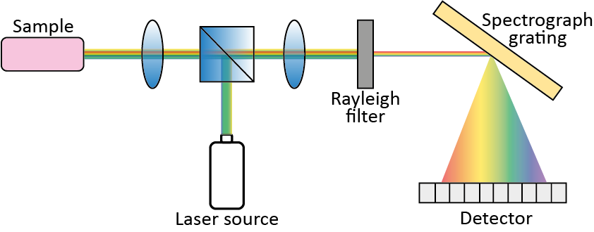
An array detector provides many pixels, laid out in a linear or two-dimensional format. Typically, there is no need for an array with a 1:1 (squared) aspect ratio in dispersive Raman spectroscopy, since the diffraction element spreads Raman wavelengths across a spectrum of lines. Hence, a linear array simplifies the whole system architecture because, by confining all detectors in a defined area, the electronics can be implemented aside, thus not impairing the Fill-Factor (FF), when considering standard planar technologies. FF is a fundamental figure of merit related to the SPAD active area, the pixel geometry, and the pixel array layout, and it is defined as the ratio between the detection active area and the total area illuminated by Raman light. Figure 6a,b underline the difference between a classical architecture with in-pixel electronic, usually employed in near 1:1 aspect-ratio arrays, and out-of-pixel electronics, more suitable for linear arrays. Out-of-pixel electronics also allows achieving a significantly smaller pixel pitch, thus increasing spatial resolution. As shown in Figure 6c, in a linear Raman array, the required number of pixels in the longer dimension, i.e., number of columns, depends on the number of spectral lines to be discriminated (i.e., wavenumber) and on the desired spectral resolution. These two parameters are specific for each Raman application and sample and depend on the optical system. The latter also defines the desired number of SPAD rows, that should match the transversal photon distribution given by the optical grating. In other words, more SPADs can be arranged in the same column pixels to increase the detected signal without losing in spectral resolution.
Figure 6. Example of (a) in-pixel and (b) out-of-pixel electronics for generic linear arrays, and (c) column pixels (associated to Raman lines) with out-of-pixel electronics for Raman linear arrays.
In-pixel electronics is no more an FF limitation when considering a 3D-stacked approach, where a top-tier includes SPADs fabricated in an optimized CMOS Image Sensor (CIS) process, while all processing electronics is implemented in a bottom-tier chip in a more scaled-down technology [
53].
Discussing spatial resolution, the minimum distance between adjacent SPADs benefits from advanced isolation techniques, such as deep trench isolation (DTI) [
54], which guarantees voltage isolation, parasitic reduction, and crosstalk minimization with narrow clearance among SPADs. Eventually, detector spatial resolution and pixel pitch directly translate into spectral resolution of Raman shifts.
Obviously, besides FF, high photon detection probability (PDP), defined as the ratio between detected and incident photons within the active area, is a key parameter to maximize photon detection. PDP is intrinsically related to the SPAD; FF depends on the array layout; the product of the two gives the overall photon detection efficiency (PDE). In Raman spectroscopy, the relative position of Raman bands with respect to the excitation frequency is independent of the excitation frequency itself. Therefore, the designer should choose an excitation frequency where the PDP is maximum. For further improving FF, hence PDP, a microlenses array (MLA) can be employed to precisely focus light onto the active areas.
The most relevant SPAD noise contribution is given by dark-count-rate (DCR) events, i.e., intrinsic avalanche generation rate of the detector in absence of illumination. A good quality fabrication technology, reducing lattice defects and minimizing generation-recombination centers [
55], is essential to improve detector noise. In large-size arrays, it is common to find some “hot pixels”, which are pixels showing a DCR much higher than the median DCR of the array, usually related to local defects. Since their presence negatively impacts the imager performance, the array should embed a way to selectively disable them during an initial configuration. However, in TG SPAD arrays, the gate on/off duty-cycle helps decreasing the probability of detecting dark counts [
51].
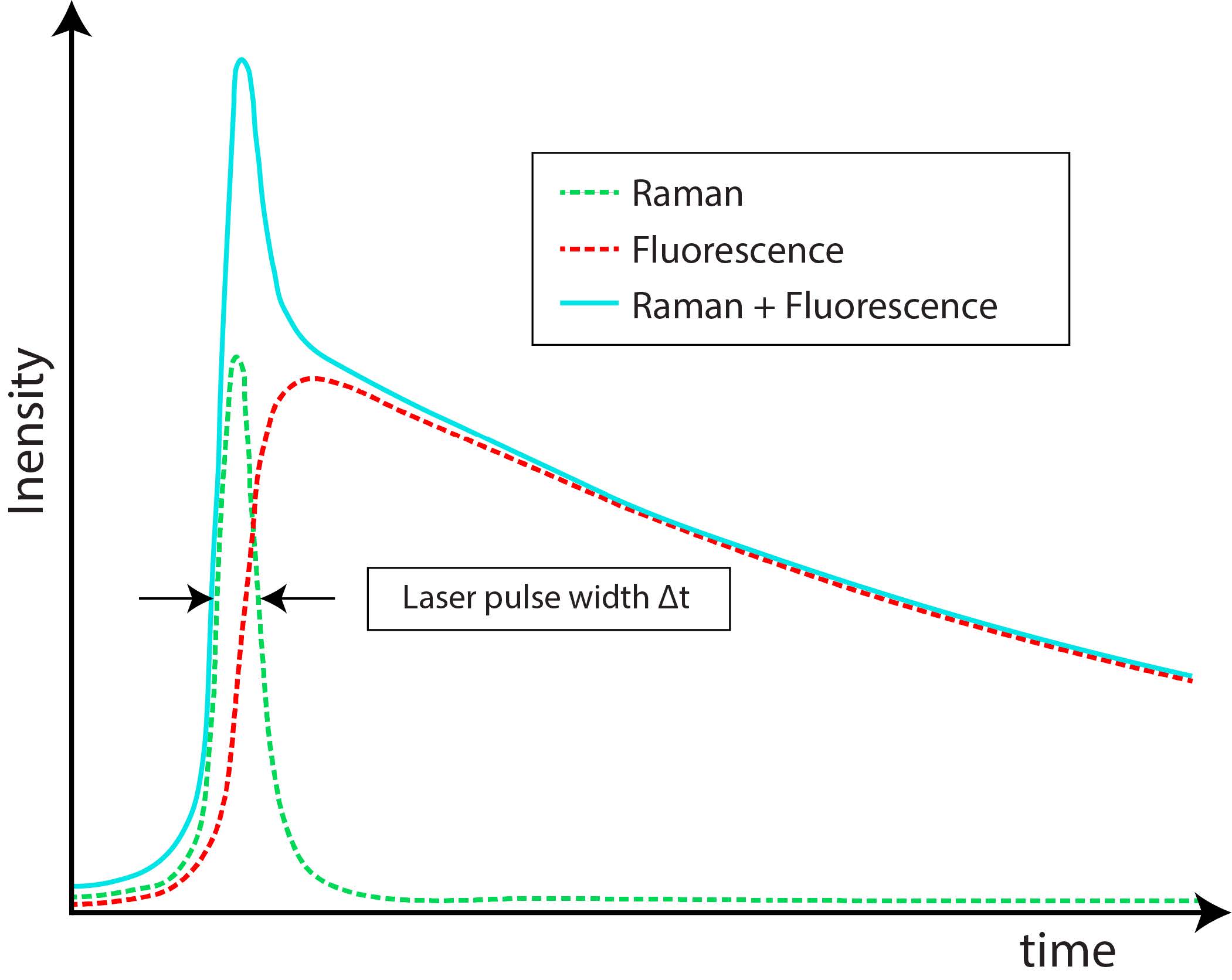
Combining a picosecond excitation pulse with a sub-nanosecond TG allows an effective main rejection of the broad unwelcome fluorescence. The rejection degree is roughly proportional to the ratio between fluorescence time constant and gate width [
56], which should ideally match the laser pulse width to maximize the collection of Raman photons scattered during the pulse, but reject the delayed fluorescence. Indeed, different gate widths and positions determine signal-to-noise ratio (SNR) changes according to:
where
NR,
NF, and
NDCR are the numbers of detected Raman, fluorescent, and dark count photons, respectively, during time-gating [
57].
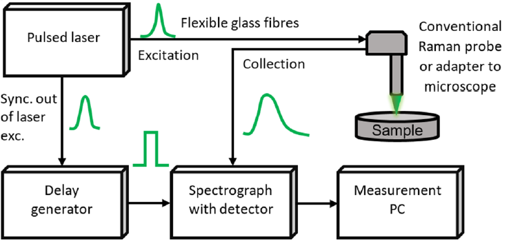
In this regard, fast and precise detector gating capability is needed. Two different approaches are possible: “hard-gating” and “soft-gating”. In “hard-gating”, SPADs are disabled outside the gate window, by biasing them below the breakdown voltage through additional transistors in their front-end circuitry, that therefore should provide both a fast activation and deactivation of the SPAD [
58]. In “soft-gating”, SPADs are not actively disabled, but the front-end’s digital output is masked to the subsequent processing electronics or, in other words, the counting or timing logic is disabled outside the gate window. In this case, rising and falling edges of the activation signal are only limited by the speed of the logic gates. In both approaches, the electronic blocks generating gate signals should be carefully designed to minimize time skews, which cause gate shifts and gate-width variations across array positions (i.e., wavelength points), becoming even larger when the number of SPADs in the array increases. This detrimental effect would give a different photon count at different spectral points even if the signal intensity remains the same [
59]. To avoid distortion in the detected Raman spectrum, it is important that all pixels get activated in the same time interval, perfectly synchronized with Raman signal. [
59] also computes signal-to-RMS-distortion ratio to define the quality of the spectra. Conversely, when fluorescence is rejected by post-processing time-to-digital converter (TDC) data, slower and less precise gate signals are needed if TDC resolution is enough to distinguish Raman and fluorescent photons. Also in this case, time skews related to TDC signals (e.g., delay lines and clocks) should be minimized, since they could affect the conversion precision. However, the TDC-based approach has the disadvantages of requiring a TDC per pixel, storing only one photon per pixel per time-frame, and slowing down the readout phase.
With high-performance timing electronics, the bottleneck could be set by the intrinsic SPAD performance, namely time-jitter and exponentially decaying tail [
60]. Time-jitter refers to the statistical distribution of delays from the actual photon arrival to the actual detection time. Instead, the exponential tail is given by photons absorbed in the neutral region (instead of the high electric field depleted region of the SPAD junction), able to trigger avalanches after a not negligible delay from the actual photon absorption: it depends both on light wavelength and SPAD cross-section. Moreover, high excess bias is beneficial because it increases the avalanche current, which can be more precisely detected by the sensing electronics [
61]. The obvious effect of these non-idealities is the time spreading of the SPAD ignition, thus the need of expanding the gate duration to match both laser width and SPAD jitter, thus increasing the detection of fluorescent photons present within the time gate and deteriorate the SNR according to (1).
When a photon is absorbed and the avalanche is triggered, the SPAD sensing and quenching circuit stops the current, preventing power dissipation, and restores the SPAD initial conditions after a given hold-off time [
44]. The latter is necessary to release the charge trapped inside the junction, if any, that could retrigger the SPAD if brought above breakdown too soon, thus giving false events correlated to the primary ignition, called afterpulses [
62]. Hold-off times in the 20–50 ns range are enough to limit afterpulsing to less than 1% in Si SPADs.
The gating frequency should be sufficiently high to repeat the laser excitation to collect a sufficient number of Raman photons within a reasonably short measurement time. At the same time, the repetition rate should be reduced to limit the overall system power consumption. The latter, indeed, is strictly related to the risk of overheating and consequently DCR increasing. If the chip temperature is kept limited without the need of a cooling system, the portability and compactness of the complete system is not compromised. Furthermore, TG inherently leads to significant dynamic power consumption, above all in the case of very fast on/off transitions applied to detectors with large capacitive loading. Therefore, particular care should be given to minimize cross-conduction currents (e.g., due to non-perfect synchronism between the signals that turn on and off the SPADs) and static power consumption due to leakage currents.
Finally, the array readout architecture plays an important role in achieving high frame-rate, hence short overall measurement time. For example, a double-buffered readout allows to perform a new acquisition while the previous data is being transferred to the on-chip electronics or to off-chip processing, virtually eliminating the typical dead time of global shutter.


