+1 credit
| Version | Summary | Created by | Modification | Content Size | Created at | Operation |
|---|---|---|---|---|---|---|
| 1 | Antonio Alessio Leonardi | + 5544 word(s) | 5544 | 2021-02-16 05:01:48 | | | |
| 2 | Vivi Li | Meta information modification | 5544 | 2021-02-23 07:09:42 | | |
Video Upload Options
Silicon is the undisputed leader for microelectronics among all the industrial materials and Si nanostructures flourish as natural candidates for tomorrow’s technologies due to the rising of novel physical properties at the nanoscale. In particular, silicon nanowires (Si NWs) are emerging as a promising resource in different fields such as electronics, photovoltaic, photonics, and sensing. Despite the plethora of techniques available for the synthesis of Si NWs, metal-assisted chemical etching (MACE) is today a cutting-edge technology for cost-effective Si nanomaterial fabrication already adopted in several research labs. During these years, MACE demonstrates interesting results for Si NW fabrication outstanding other methods. A critical study of all the main MACE routes for Si NWs is here presented, providing the comparison among all the advantages and drawbacks for different MACE approaches. All these fabrication techniques are investigated in terms of equipment, cost, complexity of the process, repeatability, also analyzing the possibility of a commercial transfer of these technologies for microelectronics, and which one may be preferred as industrial approach.
1. Introduction
In the last half-century, microelectronics and telecommunications have completely changed our world. The two application fields have in common the use of silicon (and silicon oxide) technology for both integrated circuits and optical fibers. The huge abundance on earth combined with its low-cost and its good electrical properties made the Si extremely advantageous compared to other semiconductors. Moreover, the stability, the easy and finely controlled realization of silicon oxide have determined the arising of Si as the leading material of the current technology, even outstanding germanium. Since 1970, we saw the doubling of Si transistors inside the same integrated circuit area approximately every 2 years. This technological trend was discovered by Moore, and is known as Moore’s law [1][2][3]. However, the trend has started to change in the last decades, reaching the saturation regime due to the complexity of a further down-scaling.
Nowadays, one of the strictest limits is represented by the interconnection bottleneck. The dimension decrease implies longer and so, more power- and time-consuming interconnections, in addition to a more complex circuit realization [4]. The interconnection bottleneck due to RC delays limits the advantages of device downsizing, hindering their further downscaling. These issues are not the concern of a future challenge but are already present today.
The arising of new physical phenomena on the nanoscale promoted the emerging of Si nanostructures for the past, present and future technologies. In particular, silicon nanowires (Si NWs) developed as a novel resource in many different fields, such as electronics [5][6][7], photovoltaics [8][9][10], photonics [11][12][13], and sensing [14][15][16], as schematized in Figure 1.
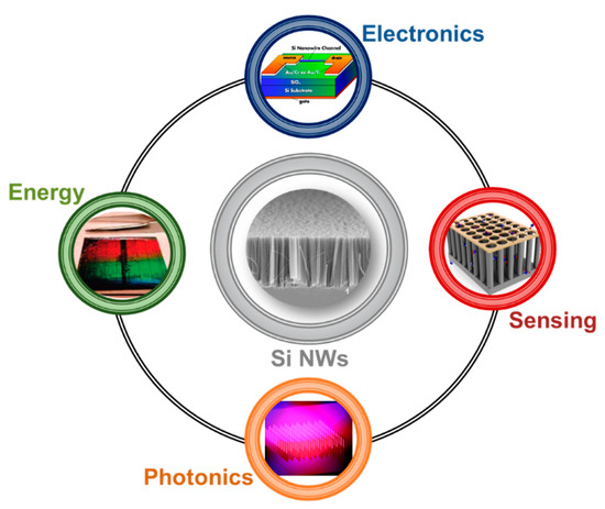
Figure 1. Schematic showing the main application fields of silicon nanowire from the top corner to the left one in clockwise order: Electronics with a Si NW Field-Effect Transistor [7], Sensing with a Si NWs-based gas sensor [16], Photonics with Si NW luminescence [11], Energy with a solar cell based on a vertically-aligned Si NWs array [8]. Top [7] and right [16] images are reproduced with permission, Copyright 2005 and 2011, IOP Publishing. Bottom [11] and left [8] images are reproduced with permission, Copyright 2010, American Chemical Society.
Indeed, 1D nanostructures can be easily integrated in the typical flat architectures of integrated circuits, benefitting from such nanomaterials’ advantages.
During these years, a lot of effort was spent on the realization of novel Field Effect Transistor (FET) based on Si NWs [17][18][19], as well as on the integration of silicon photonics in microelectronics industries [11][20][21]. Metal Oxide Semiconductors Field Effect Transistor (MOSFET) technology’s constant miniaturization for microelectronics led scientists to design new improvements based on nanomaterials, such as nanowires and nanotubes. Si NWs arise as a natural candidate, and Lieber’s group [5] showed their substantial advantages on the state-of-the-art of planar silicon FET transistors. Their Si NW FET was obtained using the same planar geometry on a silicon bridge between the source and the drain. The FET was realized with p-type Si NWs having diameters of 10–20 nm dispersed on a 600 nm silicon oxide layer on top of a silicon wafer. Moreover, the paper of Feng et al. [6] reports a low-frequency noise behavior of Si NW FET compared to the planar standard due to the electrons quantum confinement in 1D. As an example of a typical Si NW FET architecture, the device obtained from Koo et al. [7] is shown at the top of Figure 1.
2. Silver Salt and Single Step MACE
In 2002 Peng et al. realized a high density of vertically aligned Si NWs with the MACE by using an AgNO3:HF aqueous solution in a teflon-lined stainless-steel autoclave [22]. After three cleaning steps in acetone, ethanol, and diluted aqueous HF solution to remove organic grease and native oxide, the cleaned wafer was etched with 5.0:0.02 M solution of HF:AgNO3 and treated at 50 °C for 60 min. During the etching process, the silicon wafers showed the formation of a thick layer of Ag dendrites on top of the nanowires, which is promptly removed by nitric acid solution (70%). Indeed, due to the formation of silver precipitates and to the use of AgNO3, this method is commonly known as the silver salts approach and it is identified as the main single step MACE approach.
In Figure 5a–d the scheme of the silver salt process is shown in detail. After the cleaning procedure, the sample is immersed in an aqueous AgNO3:HF solution (Figure 5a). When in solution, the AgNO3 catalyst precipitates forming Ag nanoparticles (NPs) which are randomly distributed onto the silicon flat surface, catalyzing the HF driven Si etching in a very similar way to the one described for H2O2. Indeed, AgNO3 acts both as an oxidant and as a metal source. Ag NPs, with dimensions and density related to the starting silver nitrate solution, precipitate onto the Si surface biasing the etching. The Ag nanoparticles formed in solution are more electronegative than the Si and inject holes into the substrate that is oxidized due to the presence of radical NO−3. The selective oxidation process is driven at the Ag NPs/Si interface resulting in the formation of SiO2 underneath the metal NPs, and the etching continues by the HF presence, resulting in the formation of Si nanowires in the Si uncovered regions. As a byproduct of the process, Ag dendrites are formed onto the newly etched Si NWs as depicted in the scheme in Figure 5b. The Ag dendrites form a dense network of several microns thick (about 40 µm) onto the Si NWs, as displayed in the SEM cross-section (Figure 5d). Finally, the silver dendrites in excess are selectively etched by nitric acid (Figure 5c) and the Si NWs vertical array are obtained as shown from the SEM cross-section (Figure 5e).
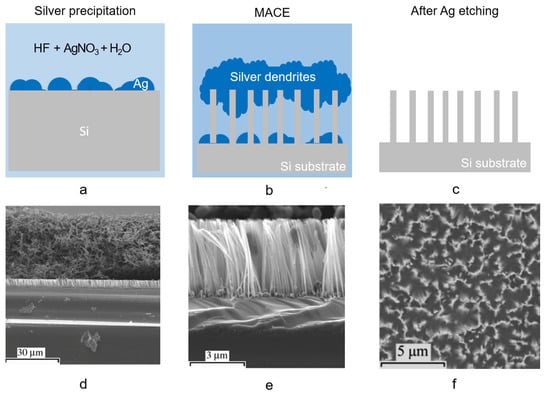
Figure 5. Scheme of Si NWs synthesis by silver salt single step MACE: (a) Ag precipitation from the HF/AgNO3 solution onto the Si surface, (b) Ag dendrites and Si NW formation, (c) Ag dendrites removal by nitric acid. Cross-section SEM of Si NW realized onto p-type (111) by HF/AgNO3 single step MACE for 30 min, (d) during Ag dendrites formation, and (e) after its removal [23]. (f) SEM plan view of Si NWs produced by HF/KAuCl4 synthesis after 30 s [24]. (d,e) ref. [23] are reproduced with permission, Copyright 2006, John Wiley and Sons. (f) ref. [24] is reproduced with permission, Copyright 2005, John Wiley and Sons.
Figure 5e shows the typical cross-section of Si NWs realized by using a HF/AgNO3 solution for 30 min with concentrations of 4.6/0.02 M. The Si NWs were obtained onto a (111) p-Si substrate preserving their crystalline quality, and are about 4 µm long [23]. The average diameter of NWs realized by single step approaches is about 70 nm ± 20 nm [25] as usually obtained by the silver salt approach, ranging from about 60 nm up to 140 nm on average [26]. As already stated, the length of the NW array can be increased with the etching time from a few hundreds of nm up to several tens of microns, leading to nanostructures with an aspect ratio above 200 [27]. Aside from AgNO3 precursors, also KAuCl4 is widely diffused for the single step MACE process. The SEM plan-view of Si NWs obtained by MACE with HF/KAuCl4 with concentrations ratio of 6.0/0.005 M after 30s, as shown in Figure 5f [24].
This single step silver salts MACE process is fast, does not need complicated sample preparation, and is less expensive than the other MACE procedures. In their pioneering works, Peng et al. investigated the strong correlation of the growth parameters, mainly the solution type and concentration, growth temperature, illumination, and substrate orientation.
Indeed, a variety of oxidative metal-based solutions can be used to drive the Si etching, such as AgNO3 [28][29], KAuCl4 [24], Fe(NO3)3 [30], KMnO4 [31], KBrO3 [32], K2Cr2O7 [31], and so on, however Ag and Fe-based oxidants presents the lowest redox potential [33]. Additionally, different noble metals such as Ag, Pt, Fe, Pd, and Au are mainly used to catalytically reduce H2O and O2 [34][35][36]. In general, dendrite structures are produced during the oxidation and dissolution of the Si substrate when the metal ions are reduced to particles, resulting in the formation of vertically aligned Si NWs with differences in the oxidation and etching rate, and for the NW morphology [33]. Higher concentrations of the metal salts result in a denser metal catalyst, hence forming nanowires with lower density, smaller diameter, and more spaced within each other. Indeed, it is not simple to control the NW planar arrangement by this approach, since their diameter, density, and interspacing are determined by the metal concentration.
Another parameter highly affecting the morphologies of the etched NWs is the type of noble metal used during the MACE. Usually, Ag and Au nanoparticles formed in solution result in straight pores during the etching, while straight or helical pores can be achieved by Pt catalyst were reported by Tsujino et al. [37][38]. Indeed, through its precipitation, Pt nanoparticles move randomly during the etching, resulting in curvy pores without a uniform etching direction. Moreover, the formation of porous nanostructures is also influenced by metal. Generally, Au-coated or Ag-coated substrates result in smoother NWs with low porosity, while Pt-driven synthesis results in a more porous structure [37]. Similarly, while standard p and n doping results in a similar etching rate for the formation of low porosity NWs, the presence of a high concentration of dopants (around 1020 dopant atoms × cm−3) for p++ and n++ Si wafers results in the formation of highly porous Si NWs due to the occurrence of lateral etching.
Peng’s MACE synthesis is a single step approach for the easy and fast formation of Si nanowires without the need of a second etching step in other oxidizing species such as H2O2 [39] or thin film depositions [40].
In general, this process is carried out at room temperature although the correlation between the temperature and the etching rate structure was also studied. The NW length approximately follows a linear trend with time. However, the etching rate also depends on the temperature and increases linearly between 0° to 50 °C [41]. Another parameter affecting the etching rate is illumination. If the intensity of illumination is sufficiently high so that the injection of the photoexcited holes is comparable or higher than the concentration of holes injected from the oxidant species, then the etching occurs faster. Studies revealed that the process is independent of the room illumination within a confidence of 5%, but an increment of about 1.5 times the etching rate was observed under light illumination with a 20 W lamp [42].
To control the axial orientation of vertically aligned Si nanowires it is possible to vary the Si wafers with other orientations, such as (100) and (110). According to the back-bond breaking theory [43][44], the (100)-orientation presents the lowest bond energy and so (100) wafer are preferentially etched vertically along with this orientation. In contrast, an atom on the (110) and (111) have three back-bond to break, hence the etching occurs again preferentially along the (100) when the etching rate dominates on the oxidation process. On the contrary, increasing the oxidant concentration favors the etching of non-(100) orientation resulting in tilted nanowires [45][46][47].
However, a crucial drawback compared to the other MACE approaches is that during the process the presence of Ag dendrites is attested onto the samples and the dendrites etching may damage the Si NWs, resulting also in Ag contaminants [48]. Hence, the MACE single step methods allow to achieve high yield, fast production rate at the expense of a lack of control on the NWs planar arrangement and diameter control [23].
Indeed, more advanced syntheses were optimized by using masked approaches, granting also the control on the NWs diameter and planar arrangement (density and spacing) by using single-step MACE coupled with lithography processes.
As an example, Nassiopoulou et al. used UV photolithography onto p-type (100) Si wafers with resistivity ranging of about 1 Ω × cm to open square-shaped windows ranging from 2 × 2 μm2 to 400 × 400 μm2 with the AZ5214 photoresist applied by spin coating, as shown in Figure 6a,b. Then, Si NWs were grown by MACE in a AgNO3/HF/H2O solution with a concentration ratio of 0.67 g:35 mL:182 mL at a temperature of 30 °C, as reported in Figure 6c. Figure 6d shows the top-view SEM microscopies imaged of the exposed windows where Si NWs are grown, confirming the efficiency of this approach. The SEM cross-section reported in Figure 6e,f shows that it is possible to grown 15 µm long vertically aligned Si NWs with good quality even at the window edge, confirming the robustness of two-steps MACE methods. Nonetheless, photolithography is limited to small areas of about 104 µm2 [49], and other approaches based on two step MACE using films achieved by the metal deposition onto silica bead can also be used [50].
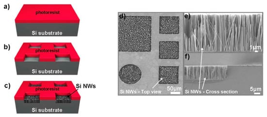
Figure 6. Flow chart for Si NW formation by MACE at a temperature of 30 °C on the confined areas by (a) applying AZ5214 photoresist, (b) opening windows from 2 × 2 μm2 to 400 × 400 μm2, and using (c) AgNO3/HF/H2O solution with a concentration ratio of 0.67 g:35 mL:182 mL. (d) Plan-view and (e,f) Cross-sections SEM images of the etched confined areas [49]. This figure [49] is reproduced with permission (open access), Copyright 2011, Springer Nature.
The primary catalysts for MACE are Ag, Au, and Pt because of their stability and catalytic activity in HF/ H2O2 solution, but apart from their high cost, the main drawbacks of these noble metals are their diffusivity in Si, which is detrimental to the performance of CMOS [51]. As an alternative W and Ni can also be used. Both W/H2O2 and Ni/H2O2 result in a lower etching rate compared to noble metal, the first one allowing the production of very large holes up to 800 nm in diameter and the latter resulting in the formation of pyramidal etched structures [52].
Gallium and Platinum ions deposited by focused ion beam can also be adopted for the Si MACE [53] and the produced NWs show poor morphology and low reproducibility.
Ti metal was also introduced to HF/ H2O2 aqueous etchant to etch Ag-loaded Si (n-type, 100) [54], resulting in a lower etching rate by increasing Ti concentration. This decrease was attributed to the lowering of H2O2 concentration because TiF62− produced by the reaction of Ti and HF can complex with H2O2 to form anions of [TiF6(H2O2)]2−.
Similar to AgNO3, also AgO (insoluble) [55] and Ag2O (soluble) [56] have been utilized instead of AgNO3 in one-step MACE always forming Ag dendrites as a byproduct. The activation energy of Si etching for HF/AgO and HF/Ag2O are lower smaller than HF/AgNO3, being 0.20 eV in HF/AgO etchant [55], and 0.15 eV in HF/Ag2O etchant [56].
The same MACE techniques used for Si NWs synthesis can also be used for the production of Si microstructures [57], and 3D structures [58].
Si microstructures are easily obtained in a sequence of steps that include selective MACE Si NWs in pre-patterned regions by masked photolithography, which are then sacrificed in an over-etching process leaving the microstructures standing. Si microstructures first synthesis step consists of the patterning realization on Si wafer by photolithography, deposition of noble metal catalyst for MACE in HF/oxidants solution to produce Si nanowires only in the patterned areas, and then etching away the Si nanowires in a KOH-based solution [59]. To allow the MACE processing, noble metal (mainly Ag, Au, and Pt) can be deposited onto the Si surface by different methods which include thermal evaporation [60][61], sputtering [47], electron beam evaporation [27], electroless deposition [24] and spin coating [62]. The whole process can be carried out at room temperature without complex equipment or special facilities, and it can be applicable on a wafer-scale.
3. Metal Film or Two Step MACE
In the literature it is possible to find both the name of metal film and thin film approaches for several types of two step MACE routes. In this paragraph will be presented all the methods reporting the use of metal film in the literature.
Metal film can be deposited on Si wafer and used as a metal catalyst in a MACE approach. Several works report the use of metal film to offer several advantages in terms of geometry control, diameter, spacing, and density [27][47][61][63][64] compared to MACE approaches that involve layers of nanoparticles similarly to single step MACE (e.g., the silver salts). The metal geometry determines the formation of silicon nanostructures and self-assembly methods can also be used for masking. Most of the approaches take advantage of metal films integration with some masking methods to strictly determine the geometry of the metal array (negative mask of the silicon nanowire array). Indeed, to surpass the lack of control in the Si NWs array geometry, the MACE can be coupled with self-assembly or a lithography process by using ordered metal film as catalysts. This method can be used to realize several silicon nano- and microstructures with a very high aspect ratio, surpassing the limit of 50:1 typical of DRIE. Different groups [65][51] report the use of MACE by high control patterned metal films (usually obtained through EBL) for nano and microfabrication of silicon. This approach can be used to fabricate Si gratings [65], honeycomb array [66] and other microstructures [67][68] or vertical aligned [33][51][63][69], tilted [46][70][71][72], zigzag [73][74][75], or tapered Si nanowires [76].
A typical approach is the one of Miao et al. [66] used to realize a silicon honeycomb array. This array was obtained by depositing the metal in a previously patterned resist, in this case, exposed and developed by UV lithography. After the lift-off, the metal results structured as the negative of the resist mask. After a typical MACE process at room temperature in a HF/H2O2 bath (H2O2 30 wt.%, HF 40wt.%), they obtained a honeycomb array of 50 µm width and 280 µm deep [66].
Another possible approach reported by Li et al. [65] consists of patterning the metal (Ti-Au) through an RIE process. Initially, a 3 nm of Ti as an adhesion layer and 20 nm of Au is deposited by EBE in a Si substrate. The sample is then spun with PMMA and patterned through EBL. The pattern realized through EBL corresponds to the final structure. In fact, the exposed metal is then etched by RIE and then the PMMA is removed. Finally, the sample is immersed in a H2O2:HF solution with the hydrogen peroxide used as an oxidation agent and a high aspect ratio is obtained with Si structures characterized by a length of 250 nm and a height of 21 µm.
Yeom et al. report the use of nanosphere lithography for the fabrication of Si NWs through MACE as visible in Figure 7 [77]. In particular, in Figure 7a the schematic of the nanosphere lithography for the realization of the Ti/Au metal film used as a catalyst is shown. After the reduction of the nanosphere dimension by RIE a Ti adhesion layer of a few nm was deposited and then followed by 10–25 nm of Au deposition. In Figure 7b–d, the main possible issues related to the nanosphere etching by RIE are reported. Figure 7b shows that a continuous RIE reduction can increase the roughness of the nanospheres or it can ruin the starting spherical shape (Figure 7c). Another issue is the formation of a continuous metal film (Figure 7d) that completely covers the nanosphere, making the lift-off process very difficult. Finally, in Figure 7e the authors show that as a function of the etching solution main parameters is possible to obtain tapered and porous Si NWs.
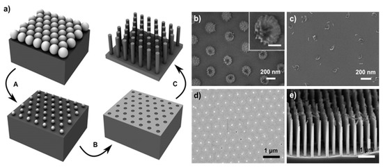
Figure 7. (a) Scheme of the Si NWs fabrication by nanosphere lithography coupled with MACE. In particular: (A) nanosphere reduction, (B) lift-off process, and (C) metal-assisted chemical etching. SEM images of the main issues and challenging steps of the process: (b) roughened nanosphere due to the RIE etching, in the inset a single roughened nanosphere is shown with a scale bar of 100 nm; (c) nanosphere shape ruined after excessive RIE, (d) unsuccessfully lift-off of an Au layer, (e) tapered and porous Si NWs by MACE [77]. This figure [77] is reproduced with permission, Copyright 2013, John Wiley and Sons.
Several types of masking procedures are being used during these years besides the elicited EBL. Wendisch et al. report on the use of colloidal lithography followed by a plasma treatment to reduce the nanosphere size [78]. Kim et al. [63] demonstrate the use of an anodic aluminium oxide mask also used in several other works [79][80]. Other types of diffused masking procedures are polystyrene spheres [61], laser interference lithography [81], superionic solid state stamping [70], and block copolymer lithography [27][82], and even Focused-Ion Beam (FIB) [53].
Despite masked approaches permits to achieve a high control on the Si structure geometry, quantum confined Si NWs remain very complicated to be obtained due to the required resolution of few nanometers. Different authors [12][51] demonstrate the application of MACE without masking approaches. To surpass the common diameter limitations, the group of Irrera engineered a metal film approach by using few nanometers of Au or Ag discontinuous layers. By the percolative self-assembly of the gold obtained at the right deposition condition, this method permits to obtain Si NWs with an average diameter of few nanometers and with a very high density. In this case, no masking procedures are applied and the NWs geometry is determined by the negative development of the percolative gold geometry.
As shown in Figure 8a–d, a discontinuous thin metal film is deposited by EBE on an oxide-free Si substrate (Figure 8a,b). The sample is then immersed into a watery solution of H2O2:HF (around 0.44 M:5 M) with the metal that drives the Si oxidation and so the etching by the HF (Figure 8c). Silicon nanowires are realized on the uncovered region, and the gold is finally removed by a gold etchant solution (Figure 8d). All the processes are performed at room temperature. The presence of the gold is not attested inside the Si NWs by using Energy Dispersive X-ray analysis and Rutherford Backscattering Spectrometry [83][84].
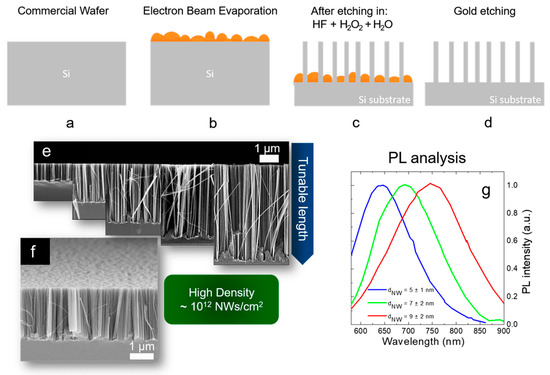
Figure 8. Scheme of Si NW synthesis by thin film MACE: (a) native oxide etching, (b) thin metal film deposition by EBE, (c) metal-assisted chemical etching, (d) gold etching. All the processes are performed at room temperature. (e) Cross-section SEM images showing the possibility to tune the NW lengths from hundreds of nanometers to several micrometers. (f) Tilted Cross-section SEM showing the high NW density of about 1012 NWs/cm2. Raman analysis of the first order stokes silicon peak. The average Si NW diameter is obtained for each different metal by fitting the Raman peak with the Campbell-Fauchet model [85]. (g) Normalized PL spectra of the different NW samples.
As shown in Figure 8e, by changing the etching time the Si NW length varies from a few hundreds of nanometers to several micrometers. Therefore, as visible in Figure 8f the density of the Si NWs is huge (about 1012 NWs/cm2) and this is a crucial point for all the applications. NW walls are smooth and with high crystalline quality, as previously observed by TEM [84]. The average diameter of these synthesized Si NWs is determined by the thickness and the type of metal used as a catalyst. In fact, the thin metal layer is discontinuous and nanometric areas of uncovered silicon are present. The average dimension of these areas is determined by the material wettability and thickness. By using 10 nm of Ag, 2 nm of Au, and 3 nm of Au an average uncovered Si diameter of 12 nm, 9 nm, and 7 nm, was respectively demonstrated. These data were obtained from the statistical analysis performed on the SEM characterizations of the different films. The dimension of the diameters of these uncovered Si holes is strictly related to the final Si NW average diameters.
In particular, for the different metal thin films, the Si NW average diameters were obtained through Raman analyses. Indeed, the Raman signals of the Si are asymmetrical due to the quantum confinement effect, and fitting them with the Campbell-Fauchet method [85] is possible to obtain the average NW diameter for each used metal. Average diameters of 10 nm, 7 nm, and 5 nm were obtained by using 10 nm of Ag (red line), 2 nm of Au (blue line), and 3 nm of Au (green line), respectively. These diameters were further confirmed by an accurate statistical TEM analysis. These NW diameters are enough to present quantum confinement effect. The emission of all the samples is reported in Figure 8g, demonstrating their quantum confinement nature. In fact, the PL is redshifted by increasing the average diameter of the Si NWs, in perfect agreement with quantum confinement theory [86][87].
A possible drawback for this MACE approach is the lack of order. However, the desired geometry that can be obtained by a masking procedure. However, this thin metal film approach is cost-effective to obtain vertically aligned and room temperature luminescent Si NWs.
Different metals were employed in these years as a catalyst during a MACE approach such as Ag [63][84][88][89], Au [65][86][51][66], Pt [53], Ni [52], Cu [74], W [51]. The most used one remains the gold due to the best quality of fabricated Si NWs, for the stability in the etching solution compared to the silver, and for the fast and high tunable etching rate compared to other metals. Ti and other material such as AZO were also used as an adhesion layer for thick Au films, permitting to improve the film stability [77][78][90]. Kim et al. report the application of an Au/Ag bilayer mesh to avoid the issue on the Ag stability and anodic dissolution during the etching [63]. Wendisch et al. used an AZO reporting an improvement in the homogeneity of the etching and the possibility to vary the etching rate by changing its thickness [78]. The same group and also Yeom et al. [77] report gold delamination for high H2O2 concentrations (e.g., for 10:1:10 HF/H2O2/H2O) and for in general high etch rates (>400–600 nm/m) and small thin films (<20 nm) [78]. The dependence on the etching rate is confirmed by other works [65] and it is reasonable to assume that metal instability may be also affected by the wafer pre-treatment and deposition type. The etching rate is the key parameter, and a too fast process can be unstable and not affordable in terms of reproducibility. Indeed, in our experiment using few nanometers of Au we never observed gold delamination or large area defects in the Si NW array by an etching rate of 460 nm/min and a solution of HF (5 M) and H2O2 (0.44 M). The role of a high concentration of H2O2 is clear because it can increase the hole injection and reaction at the metal silicon interface, thus increasing the bubble formation during the etching possibly affecting the metal stability. These effects and issues regard the use of a connected Au film.
The etching rate is influenced by the gold coverage and so by the NWs diameter. Indeed, the amount of silicon to be etched depends on the covered region of the gold template, on the pitches (average gold region between Si NWs), and on the diameter of Si NWs [78].
NW average diameter is determined by the metal film and usually ranges around 50 nm [51][63] but as seen in Figure 7 with the possibility to reach few nanometers and quantum confinement suitable dimensions [12].
The reported preferential etching direction depends on several factors as wafer crystalline orientation, used etchant/oxidant solution, and its molar ratio, temperature, and metal film type and thickness [51][71][73][78][91]. The wafer crystalline orientation has been found as the main parameter that determines the etching orientation with a preferential etching along the <100> direction [38][43][51][92][93]. However, the concentration and ratio between the etchant and oxidant (usually HF/H2O2) can lead to other orientation etching. This can be understood considering that for a starting crystalline orientation, the etching orientation is driven by the reaction kinetic. Starting from Si (100) it was demonstrated that <100> remain the etching direction at a low etching rate [63]. On the contrary, increasing the etching rate the same authors observed an etching in the <110> direction. The etching rate is characterized by the interplay of holes injection into silicon that is proportional to the metal electronegativity and to the oxidant H2O2 concentration and by the HF etching of silicon associated with the cleavage of Si back bonds [63]. Indeed, Si atom density exposed to the interface depends on the considered crystal plane [94]. At standard operation conditions, the hole injection is the limiting process of MACE. Increasing the concentration of injected holes above a certain threshold will cause the remotion of Si atoms where there is a higher concentration of Si back bonds causing in certain cases a change in the etching orientation. However, this condition requires a high enough HF concentration and the oxidant concentration as a limiting condition. Otherwise, with a Si (100) wafer, a low concentration of HF slowly etch the silicon in the <100> direction and the excess of holes diffuses causing new pore nucleation sites in presence of defect or doping atoms [51][63]. The temperature plays a role in the activation of non-<100> direction etching. Indeed, considering the same etching solution this can lead to an <100> etching at room temperature and <110> etching at higher temperatures (>50 °C for H2O2 1 M and HF/H2O2 molar ratio of about 23) [63]. Temperature control is also used to low the etching rate and so the possible lateral etching with some works that report on cold MACE synthesis performed near 0 °C [65], while other works used higher temperature above 55 °C to form zigzag Si NWs [73].
As elicited, the type of metal mesh plays a role in the etching direction. Several experiments were performed in the same etching condition by using isolated metal particles instead of connected metal films. For metal film the etching is preferentially vertical to the wafer surface due to the difficulty of horizontal movement of the film. On the contrary, metal particles or isolated islands have more degrees of freedom. Indeed, MACE has been used to realize 3D etching taking advantage of the unconstrained metal particles movement during etching at the right conditions [95][96].
Lateral etching or in general a more isotropic etching is found to happen when a large number of holes are injected at the metal-silicon interface [66][97]. The diffusion of these holes can oxidize the sidewall, and lead to a lateral etching and porous nanostructures. The porosity of Si NWs depends on the doping level of Si wafer and on the solution concentration, especially of H2O2 or other oxidant agents [51]. Heavily doped Si wafers produce more easily porous Si NWs because the doping atoms may act as nucleation centers (e.g., metal atoms in solution), catalyzing the lateral etching and the pore formations [98][99][100]. In highly doped substrates, a competition between vertical etching and lateral etching (and so porous formation) occurs [101][102]. If the vertical etching is fast enough it is possible to obtain crystalline Si NWs at the right bath condition without the formation of porous structure [51][84]. As for the crystalline orientation, there is a strong dependence on the ratio between the H2O2 (and so hole injection) and HF (and so Si atom remotion) [51].
Concerning the standard HF/H2O2 Mace bath Kim et al. reported that ethanol can be used to lower the etching rate influencing the etching direction and the final morphology [103]. This can also lead to tapered Si NWs as demonstrate by Azeredo et al. by controlling the ethanol concentration [104]. The addition of other oxidant co-solvent as methanol, isopropanol, acetonitrile, and so on has also been found as a method to change the etching orientation [103].
A final consideration is the possible agglomeration of the NWs tips as a result of a very high aspect ratio, and as a function of the drying protocol. Several works reported on the NW tips bunching for very long Si NWs [65][40]. A possible solution proposed in these years is a drying protocol that involves a final bath in isopropanol (lower capillary forces than water) followed by natural evaporation of the alcohol [65][105]. Bunching of micro and nanostructures are typical issues of MEMS. Hence another viable industrial solution for Si NWs or other microstructures is to use a critical point dryer [27][106].
Metal film MACE permits a high flexibility of use for Si NW fabrication with several routes that can be followed to change diameter, orientation, density, porous formation, and so on. As demonstrated by the current trend of publications, the MACE method is becoming an outstanding tool for Si NWs synthesis and, for certain applications able to challenge RIE approaches for Si microstructure fabrication. In the next future, this relative novel approach may be really adopted for large-scale production of Si NWs thanks to the advantage of being compatible with the current industrial standard equipment. Indeed, the low-cost of this approach coupled with the very high aspect ratio makes it really appealing for microfabrication, challenging the more diffuse and consolidated approaches as DRIE.
References
- Waldrop, M.M. More Than Moore. Nature 2016, 530, 144–147.
- Radamson, H.H.; Zhu, H.; Wu, Z.; He, X.; Lin, H.; Liu, J.; Xiang, J.; Kong, Z.; Xiong, W.; Li, J.; et al. State of the Art and Future Perspectives in Advanced CMOS Technology. Nanomaterials 2020, 10, 1555.
- Radamson, H.H.; He, X.; Zhang, Q.; Liu, J.; Cui, H.; Xiang, J.; Kong, Z.; Xiong, W.; Li, J.; Gao, J.; et al. Miniaturization of CMOS. Micromachines 2019, 10, 293.
- Cobalt Could Untangle Chips’ Wiring Problems—IEEE Spectrum. Available online: https://spectrum.ieee.org/semiconductors/materials/cobalt-could-untangle-chips-wiring-problems (accessed on 3 December 2020).
- Cui, Y.; Zhong, Z.; Wang, D.; Wang, W.U.; Lieber, C.M. High performance silicon nanowire field effect transistors. Nano Lett. 2003, 3, 149–152.
- Feng, W.; Hettiarachchi, R.; Sato, S.; Kakushima, K.; Niwa, M.; Iwai, H.; Yamada, K.; Ohmori, K. Advantages of silicon nanowire metal-oxide-semiconductor field-effect transistors over planar ones in noise properties. Jpn. J. Appl. Phys. 2012, 51, 04DC06.
- Koo, S.M.; Edelstein, M.D.; Li, Q.; Richter, C.A.; Vogel, E.M. Silicon nanowires as enhancement-mode Schottky barrier field-effect transistors. Nanotechnology 2005, 16, 1482–1485.
- Garnett, E.; Yang, P. Light Trapping in Silicon Nanowire Solar Cells. Nano Lett. 2010, 10, 1082–1087.
- Kelzenberg, M.D.; Boettcher, S.W.; Petykiewicz, J.A.; Turner-Evans, D.B.; Putnam, M.C.; Warren, E.L.; Spurgeon, J.M.; Briggs, R.M.; Lewis, N.S.; Atwater, H.A. Enhanced absorption and carrier collection in Si wire arrays for photovoltaic applications. Nat. Mater. 2010, 9, 239–244.
- Cao, L.; Fan, P.; Vasudev, A.P.; White, J.S.; Yu, Z.; Cai, W.; Schuller, J.A.; Fan, S.; Brongersma, M.L. Semiconductor Nanowire Optical Antenna Solar Absorbers. Nano Lett. 2010, 10, 439–445.
- Walavalkar, S.S.; Hofmann, C.E.; Homyk, A.P.; Henry, M.D.; Atwater, H.A.; Scherer, A. Tunable visible and near-IR emission from sub-10 nm etched single-crystal Si nanopillars. Nano Lett. 2010, 10, 4423–4428.
- Leonardi, A.A.; Nastasi, F.; Morganti, D.; Lo Faro, M.J.; Picca, R.A.; Cioffi, N.; Franzò, G.; Serroni, S.; Priolo, F.; Puntoriero, F.; et al. New Hybrid Light Harvesting Antenna Based on Silicon Nanowires and Metal Dendrimers. Adv. Opt. Mater. 2020, 8, 2001070.
- Kalem, S.; Werner, P.; Talalaev, V. Near-IR photoluminescence from Si/Ge nanowire-grown silicon wafers: Effect of HF treatment. Appl. Phys. A Mater. Sci. Process. 2013, 112, 561–567.
- Leonardi, A.A.A.A.; Lo Faro, M.J.M.J.; Di Franco, C.; Palazzo, G.; D’Andrea, C.; Morganti, D.; Manoli, K.; Musumeci, P.; Fazio, B.; Lanza, M.; et al. Silicon nanowire luminescent sensor for cardiovascular risk in saliva. J. Mater. Sci. Mater. Electron. 2020, 31, 10–17.
- Patolsky, F.; Zheng, G.; Lieber, C.M. Nanowire sensors for medicine and the life sciences. Nanomedicine 2006, 1, 51–65.
- In, H.J.; Field, C.R.; Pehrsson, P.E. Periodically porous top electrodes on vertical nanowire arrays for highly sensitive gas detection. Nanotechnology 2011, 22, 355501.
- Nah, J.; Liu, E.S.; Shahrjerdi, D.; Varahramyan, K.M.; Banerjee, S.K.; Tutuc, E. Realization of dual-gated Ge- SixGe1-x core-shell nanowire field effect transistors with highly doped source and drain. Appl. Phys. Lett. 2009, 94, 063117.
- Javey, A.; Nam, S.; Friedman, R.S.; Yan, H.; Lieber, C.M. Layer-by-layer assembly of nanowires for three-dimensional, multifunctional electronics. Nano Lett. 2007, 7, 773–777.
- Goldberger, J.; Hochbaum, A.I.; Fan, R.; Yang, P. Silicon vertically integrated nanowire field effect transistors. Nano Lett. 2006, 6, 973–977.
- Lo Faro, M.J.; Leonardi, A.A.; Morganti, D.; Fazio, B.; Vasi, C.; Musumeci, P.; Priolo, F.; Irrera, A. Low Cost Fabrication of Si NWs/CuI Heterostructures. Nanomaterials 2018, 8, 569.
- Liu, K.; Zhu, Z.H.; Li, X.J.; Zhang, J.F.; Yuan, X.D.; Guo, C.C.; Xu, W.; Qin, S.Q. Bright Multicolored Photoluminescence of Hybrid Graphene/Silicon Optoelectronics. ACS Photonics 2015, 2, 797–804.
- Peng, K.Q.; Yan, Y.J.; Gao, S.P.; Zhu, J. Synthesis of large-area silicon nanowire arrays via self-assembling nanoelectrochemistry. Adv. Mater. 2002, 14, 1164–1167.
- Peng, K.; Fang, H.; Hu, J.; Wu, Y.; Zhu, J.; Yan, Y.; Lee, S. Metal-Particle-Induced, Highly Localized Site-Specific Etching of Si and Formation of Single-Crystalline Si Nanowires in Aqueous Fluoride Solution. Chem. A Eur. J. 2006, 12, 7942–7947.
- Peng, K.; Hu, J.; Yan, Y.; Wu, Y.; Fang, H.; Xu, Y.; Lee, S.; Zhu, J. Fabrication of single-crystalline silicon nanowires by scratching a silicon surface with catalytic metal particles. Adv. Funct. Mater. 2006, 16, 387–394.
- Donato, M.G.M.G.; Brzobohatý, O.; Simpson, S.H.S.H.; Irrera, A.; Leonardi, A.A.A.A.; Lo Faro, M.J.M.J.; Svak, V.; Maragò, O.M.O.M.; Zemánek, P. Optical Trapping, Optical Binding, and Rotational Dynamics of Silicon Nanowires in Counter-Propagating Beams. Nano Lett. 2019, 19, 342–352.
- Venkatesan, R.; Arivalagan, M.K.; Venkatachalapathy, V.; Pearce, J.M.; Mayandi, J. Effects of silver catalyst concentration in metal assisted chemical etching of silicon. Mater. Lett. 2018, 221, 206–210.
- Chang, S.W.; Chuang, V.P.; Boles, S.T.; Ross, C.A.; Thompson, C.V. Densely packed arrays of ultra-high-as pect-ratio silicon nanowires fabricated using block-copolymer lithography and metal-assisted etching. Adv. Funct. Mater. 2009, 19, 2495–2500.
- Ono, S.; Oide, A.; Asoh, H. Nanopatterning of silicon with use of self-organized porous alumina and colloidal crystals as mask. Electrochim. Acta 2007, 52, 2898–2904.
- Pal, A.; Ghosh, R.; Giri, P.K. Early stages of growth of Si nanowires by metal assisted chemical etching: A scaling study. Appl. Phys. Lett. 2015, 107, 072104.
- Nahidi, M.; Kolasinski, K.W. Effects of Stain Etchant Composition on the Photoluminescence and Morphology of Porous Silicon. J. Electrochem. Soc. 2006, 153, C19.
- Nahm, K.S.; Seo, Y.H.; Lee, H.J. Formation mechanism of stains during Si etching reaction in HF-oxidizing agent-H2O solutions. J. Appl. Phys. 1997, 81, 2418–2424.
- Seo, Y.H.; Nahm, K.S.; Lee, K.B. Mechanistic Study of Silicon Etching in HF-KBrO3-H2O Solution. J. Electrochem. Soc. 1993, 140, 1453–1458.
- Huang, Z.; Geyer, N.; Werner, P.; de Boor, J.; Gösele, U. Metal-Assisted Chemical Etching of Silicon: A Review. Adv. Mater. 2011, 23, 285–308.
- Huang, J.C.; Sen, R.K.; Yeager, E. Oxygen Reduction on Platinum in 85% Orthophosphoric Acid. J. Electrochem. Soc. 1979, 126, 786–792.
- Zeis, R.; Lei, T.; Sieradzki, K.; Snyder, J.; Erlebacher, J. Catalytic reduction of oxygen and hydrogen peroxide by nanoporous gold. J. Catal. 2008, 253, 132–138.
- Flätgen, G.; Wasle, S.; Lübke, M.; Eickes, C.; Radhakrishnan, G.; Doblhofer, K.; Ertl, G. Autocatalytic mechanism of H2O2 reduction on Ag electrodes in acidic electrolyte: Experiments and simulations. Electrochim. Acta 1999, 44, 4499–4506.
- Tsujino, K.; Matsumura, M. Boring deep cylindrical nanoholes in silicon using silver nanoparticles as a catalyst. Adv. Mater. 2005, 17, 1045–1047.
- Chen, C.Y.; Wu, C.S.; Chou, C.J.; Yen, T.J. Morphological control of single-crystalline silicon nanowire arrays near room temperature. Adv. Mater. 2008, 20, 3811–3815.
- Naffeti, M.; Postigo, P.A.; Chtourou, R.; Zaïbi, M.A. Elucidating the Effect of Etching Time Key-Parameter toward Optically and Electrically-Active Silicon Nanowires. Nanomaterials 2020, 10, 404.
- Lo Faro, M.J.M.J.; Leonardi, A.A.A.A.; D’Andrea, C.; Morganti, D.; Musumeci, P.; Vasi, C.; Priolo, F.; Fazio, B.; Irrera, A. Low cost synthesis of silicon nanowires for photonic applications. J. Mater. Sci. Mater. Electron. 2020, 31, 34–40.
- Cheng, S.L.; Chung, C.H.; Lee, H.C. A Study of the Synthesis, Characterization, and Kinetics of Vertical Silicon Nanowire Arrays on (001)Si Substrates. J. Electrochem. Soc. 2008, 155, D711.
- Chattopadhyay, S.; Li, X.; Bohn, P.W. In-plane control of morphology and tunable photoluminescence in porous silicon produced by metal-assisted electroless chemical etching. J. Appl. Phys. 2002, 91, 6134–6140.
- Peng, K.; Lu, A.; Zhang, R.; Lee, S.T. Motility of metal nanoparticles in silicon and induced anisotropic silicon etching. Adv. Funct. Mater. 2008, 18, 3026–3035.
- Peng, K.; Yan, Y.; Gao, S.; Zhu, J. Dendrite-Assisted Growth of Silicon Nanowires in Electroless Metal Deposition. Adv. Funct. Mater. 2003, 13, 127–132.
- Salem, A.M.S.; Harraz, F.A.; El-Sheikh, S.M.; Ismat Shah, S. Novel Si nanostructures via Ag-assisted chemical etching route on single and polycrystalline substrates. Mater. Sci. Eng. B Solid-State Mater. Adv. Technol. 2020, 262, 114793.
- Huang, Z.; Shimizu, T.; Senz, S.; Zhang, Z.; Geyer, N.; Gösele, U. Oxidation rate effect on the direction of metal-assisted chemical and electrochemical etching of silicon. J. Phys. Chem. C 2010, 114, 10683–10690.
- Huang, Z.; Shimizu, T.; Senz, S.; Zhang, Z.; Zhang, X.; Lee, W.; Geyer, N.; Gösele, U. Ordered arrays of vertically aligned [110] silicon nanowires by suppressing the crystallographically preferred <100> etching directions. Nano Lett. 2009, 9, 2519–2525.
- Smith, Z.R.; Smith, R.L.; Collins, S.D. Mechanism of nanowire formation in metal assisted chemical etching. Electrochim. Acta 2013, 92, 139–147.
- Nassiopoulou, A.G.; Gianneta, V.; Katsogridakis, C. Si nanowires by a single-step metal-assisted chemical etching process on lithographically defined areas: Formation kinetics. Nanoscale Res. Lett. 2011, 6, 1–8.
- Weisse, J.M.; Kim, D.R.; Lee, C.H.; Zheng, X. Vertical transfer of uniform silicon nanowire arrays via crack formation. Nano Lett. 2011, 11, 1300–1305.
- Han, H.; Huang, Z.; Lee, W. Metal-assisted chemical etching of silicon and nanotechnology applications. Nano Today 2014, 9, 271–304.
- Yue, Z.; Shen, H.; Jiang, Y.; Wang, W.; Jin, J. Novel and low reflective silicon surface fabricated by Ni-assisted electroless etching and coated with atomic layer deposited Al2O 3 film. Appl. Phys. A Mater. Sci. Process. 2014, 114, 813–817.
- Hildreth, O.; Rykaczewski, K.; Wong, C.P. Participation of focused ion beam implanted gallium ions in metal-assisted chemical etching of silicon. J. Vac. Sci. Technol. B Nanotechnol. Microelectron. Mater. Process. Meas. Phenom. 2012, 30, 040603.
- Cui, L.; Xia, W.W.; Wang, F.; Yang, L.J.; Hu, Y.J. Investigations on the Si/SiO2 interface defects of silicon nanowires. Phys. B Condens. Matter 2013, 409, 47–50.
- Kato, Y.; Adachi, S. Synthesis of Si Nanowire Arrays in AgO/HF Solution and Their Optical and Wettability Properties. J. Electrochem. Soc. 2011, 158, K157.
- Kato, Y.; Adachi, S. Fabrication and optical characterization of Si nanowires formed by catalytic chemical etching in Ag2O/HF solution. Appl. Surf. Sci. 2012, 258, 5689–5697.
- Kim, S.-M.; Khang, D.-Y. Bulk Micromachining of Si by Metal-assisted Chemical Etching. Small 2014, 10, 3761–3766.
- Hildreth, O.J.; Lin, W.; Wong, C.P. Effect of catalyst shape and etchant composition on etching direction in metal-assisted chemical etching of silicon to fabricate 3D nanostructures. ACS Nano 2009, 3, 4033–4042.
- Pérez-Díaz, O.; Quiroga-González, E.; Silva-González, N.R. Silicon microstructures through the production of silicon nanowires by metal-assisted chemical etching, used as sacrificial material. J. Mater. Sci. 2019, 54, 2351–2357.
- Fang, H.; Wu, Y.; Zhao, J.; Zhu, J. Silver catalysis in the fabrication of silicon nanowire arrays. Nanotechnology 2006, 17, 3768–3774.
- Huang, Z.; Fang, H.; Zhu, J. Fabrication of silicon nanowire arrays with controlled diameter, length, and density. Adv. Mater. 2007, 19, 744–748.
- Harada, Y.; Li, X.; Bohn, P.W.; Nuzzo, R.G. Catalytic amplification of the soft lithographic patterning of Si. Nonelectrochemical orthogonal fabrication of photoluminescent porous Si pixel arrays. J. Am. Chem. Soc. 2001, 123, 8709–8717.
- Kim, J.; Han, H.; Kim, Y.H.; Choi, S.H.; Kim, J.C.; Lee, W. Au/Ag bilayered metal mesh as a Si etching catalyst for controlled fabrication of Si nanowires. ACS Nano 2011, 5, 3222–3229.
- Wang, S.; Liu, H.; Han, J. Comprehensive study of Au nano-mesh as a catalyst in the fabrication of silicon nanowires arrays by metal-assisted chemical etching. Coatings 2019, 9, 149.
- Li, H.; Ye, T.; Shi, L.; Xie, C. Fabrication of ultra-high aspect ratio (>160:1) silicon nanostructures by using Au metal assisted chemical etching. J. Micromech. Microeng. 2017, 27, 124002.
- Miao, B.; Zhang, J.; Ding, X.; Wu, D.; Wu, Y.; Lu, W.; Li, J. Improved metal assisted chemical etching method for uniform, vertical and deep silicon structure. J. Micromech. Microeng. 2017, 27, 055019.
- Zahedinejad, M.; Farimani, S.D.; Khaje, M.; Mehrara, H.; Erfanian, A.; Zeinali, F. Deep and vertical silicon bulk micromachining using metal assisted chemical etching. J. Micromech. Microeng. 2013, 23, 055015.
- Li, L.; Zhang, G.; Wong, C.P. Formation of Through Silicon Vias for Silicon Interposer in Wafer Level by Metal-Assisted Chemical Etching. IEEE Trans. Compon. Packag. Manuf. Technol. 2015, 5, 1039–1049.
- Zhang, M.L.; Peng, K.Q.; Fan, X.; Jie, J.S.; Zhang, R.Q.; Lee, S.T.; Wong, N.B. Preparation of large-area uniform silicon nanowires arrays through metal-assisted chemical etching. J. Phys. Chem. C 2008, 112, 4444–4450.
- Chern, W.; Hsu, K.; Chun, I.S.; Azeredo, B.P.D.; Ahmed, N.; Kim, K.H.; Zuo, J.M.; Fang, N.; Ferreira, P.; Li, X. Nonlithographic patterning and metal-assisted chemical etching for manufacturing of tunable light-emitting silicon nanowire arrays. Nano Lett. 2010, 10, 1582–1588.
- Kim, J.; Kim, Y.H.; Choi, S.H.; Lee, W. Curved silicon nanowires with ribbon-like cross sections by metal-assisted chemical etching. ACS Nano 2011, 5, 5242–5248.
- Sandu, G.; Avila Osses, J.; Luciano, M.; Caina, D.; Stopin, A.; Bonifazi, D.; Gohy, J.F.; Silhanek, A.; Florea, I.; Bahri, M.; et al. Kinked Silicon Nanowires: Superstructures by Metal-Assisted Chemical Etching. Nano Lett. 2019, 19, 7681–7690.
- Chen, H.; Wang, H.; Zhang, X.H.; Lee, C.S.; Lee, S.T. Wafer-scale synthesis of single-crystal zigzag silicon nanowire arrays with controlled turning angles. Nano Lett. 2010, 10, 864–868.
- Huang, Z.P.; Geyer, N.; Liu, L.F.; Li, M.Y.; Zhong, P. Metal-assisted electrochemical etching of silicon. Nanotechnology 2010, 21, 465301.
- Chen, Y.; Li, L.; Zhang, C.; Tuan, C.C.; Chen, X.; Gao, J.; Wong, C.P. Controlling Kink Geometry in Nanowires Fabricated by Alternating Metal-Assisted Chemical Etching. Nano Lett. 2017, 17, 1014–1019.
- Lin, H.; Cheung, H.Y.; Xiu, F.; Wang, F.; Yip, S.; Han, N.; Hung, T.; Zhou, J.; Ho, J.C.; Wong, C.Y. Developing controllable anisotropic wet etching to achieve silicon nanorods, nanopencils and nanocones for efficient photon trapping. J. Mater. Chem. A 2013, 1, 9942–9946.
- Yeom, J.; Ratchford, D.; Field, C.R.; Brintlinger, T.H.; Pehrsson, P.E. Decoupling Diameter and Pitch in Silicon Nanowire Arrays Made by Metal-Assisted Chemical Etching. Adv. Funct. Mater. 2014, 24, 106–116.
- Wendisch, F.J.; Rey, M.; Vogel, N.; Bourret, G.R. Large-Scale Synthesis of Highly Uniform Silicon Nanowire Arrays Using Metal-Assisted Chemical Etching. Chem. Mater. 2020, 32, 9425–9434.
- Huang, J.; Chiam, S.Y.; Tan, H.H.; Wang, S.; Chim, W.K. Fabrication of silicon nanowires with precise diameter control using metal nanodot arrays as a hard mask blocking material in chemical etching. Chem. Mater. 2010, 22, 4111–4116.
- Huang, Z.; Zhang, X.; Reiche, M.; Ltu, L.; Lee, W.; Shimizu, T.; Senz, S.; Gösele, U. Extended arrays of vertically aligned Sub-10 nm diameter [100] Si nanowires by metal-assisted chemical etching. Nano Lett. 2008, 8, 3046–3051.
- De Boor, J.; Geyer, N.; Wittemann, J.V.; Gösele, U.; Schmidt, V. Sub-100 nm silicon nanowires by laser interference lithography and metal-assisted etching. Nanotechnology 2010, 21, 095302.
- Gowrishankar, V.; Miller, N.; McGehee, M.D.; Misner, M.J.; Ryu, D.Y.; Russell, T.P.; Drockenmuller, E.; Hawker, C.J. Fabrication of densely packed, well-ordered, high-aspect-ratio silicon nanopillars over large areas using block copolymer lithography. Thin Solid Films 2006, 513, 289–294.
- Irrera, A.; Magazzù, A.; Artoni, P.; Simpson, S.H.; Hanna, S.; Jones, P.H.; Priolo, F.; Gucciardi, P.G.; Maragò, O.M. Photonic Torque Microscopy of the Nonconservative Force Field for Optically Trapped Silicon Nanowires. Nano Lett. 2016, 16, 4181–4188.
- Irrera, A.; Lo Faro, M.J.; D’Andrea, C.; Leonardi, A.A.; Artoni, P.; Fazio, B.; Anna Picca, R.; Cioffi, N.; Trusso, S.; Franzò, G.; et al. Light-emitting silicon nanowires obtained by metal-assisted chemical etching. Semicond. Sci. Technol. 2017, 32, 043004.
- Campbell, I.H.; Fauchet, P.M. The effects of microcrystal size and shape on the one phonon Raman spectra of crystalline semiconductors. Solid State Commun. 1986, 58, 739–741.
- Leonardi, A.A.; Lo Faro, M.J.; Irrera, A. CMOS-Compatible and Low-Cost Thin Film MACE Approach for Light-Emitting Si NWs Fabrication. Nanomaterials 2020, 10, 966.
- Lo Faro, M.J.; Leonardi, A.A.; Priolo, F.; Fazio, B.; Miritello, M.; Irrera, A. Erbium emission in Er:Y2O3 decorated fractal arrays of silicon nanowires. Sci. Rep. 2020, 10, 12854.
- Geyer, N.; Fuhrmann, B.; Huang, Z.; De Boor, J.; Leipner, H.S.; Werner, P. Model for the mass transport during metal-assisted chemical etching with contiguous metal films as catalysts. J. Phys. Chem. C 2012, 116, 13446–13451.
- Li, X.; Xiao, Y.; Bang, J.H.; Lausch, D.; Meyer, S.; Miclea, P.-T.; Jung, J.-Y.; Schweizer, S.L.; Lee, J.-H.; Wehrspohn, R.B. Upgraded Silicon Nanowires by Metal-Assisted Etching of Metallurgical Silicon: A New Route to Nanostructured Solar-Grade Silicon. Adv. Mater. 2013, 25, 3187–3191.
- Wendisch, F.J.; Abazari, M.; Mahdavi, H.; Rey, M.; Vogel, N.; Musso, M.; Diwald, O.; Bourret, G.R. Morphology-Graded Silicon Nanowire Arrays via Chemical Etching: Engineering Optical Properties at the Nanoscale and Macroscale. ACS Appl. Mater. Interfaces 2020, 12, 13140–13147.
- Bodo, F.; Hartmut, S.L.; Höche, H.-R.; Schubert, L.; Werner, P.; Gösele, U. Ordered Arrays of Silicon Nanowires Produced by Nanosphere Lithography and Molecular Beam Epitaxy. Nano Lett. 2005, 5, 2524–2527.
- Christophersen, M.; Carstensen, J.; Rönnebeck, S.; Jäger, C.; Jäger, W.; Föll, H. Crystal Orientation Dependence and Anisotropic Properties of Macropore Formation of p- and n-Type Silicon. J. Electrochem. Soc. 2001, 148, E267.
- Lehmann, V. The Physics of Macropore Formation in Low Doped n-Type Silicon. J. Electrochem. Soc. 1993, 140, 2836–2843.
- Sze, S.M.; Ng, K.K. Physics of Semiconductor Devices; John Wiley & Sons, Inc.: Hoboken, NJ, USA, 2006; ISBN 9780470068328.
- Hildreth, O.J.; Fedorov, A.G.; Wong, C.P. 3D spirals with controlled chirality fabricated using metal-assisted chemical etching of silicon. ACS Nano 2012, 6, 10004–10012.
- Hildreth, O.J.; Brown, D.; Wong, C.P. 3D Out-of-Plane Rotational Etching with Pinned Catalysts in Metal-Assisted Chemical Etching of Silicon. Adv. Funct. Mater. 2011, 21, 3119–3128.
- Li, L.; Zhao, X.; Wong, C.P. Deep etching of single- and polycrystalline silicon with high speed, high aspect ratio, high uniformity, and 3D complexity by electric bias-attenuated metal-assisted chemical etching (EMaCE). ACS Appl. Mater. Interfaces 2014, 6, 16782–16791.
- Qu, Y.; Liao, L.; Li, Y.; Zhang, H.; Huang, Y.; Duan, X. Electrically conductive and optically active porous silicon nanowires. Nano Lett. 2009, 9, 4539–4543.
- Zhong, X.; Qu, Y.; Lin, Y.C.; Liao, L.; Duan, X. Unveiling the formation pathway of single crystalline porous silicon nanowires. ACS Appl. Mater. Interfaces 2011, 3, 261–270.
- Balasundaram, K.; Sadhu, J.S.; Shin, J.C.; Azeredo, B.; Chanda, D.; Malik, M.; Hsu, K.; Rogers, J.A.; Ferreira, P.; Sinha, S.; et al. Porosity control in metal-assisted chemical etching of degenerately doped silicon nanowires. Nanotechnology 2012, 23, 305304.
- Chiappini, C.; Liu, X.; Fakhoury, J.R.; Ferrari, M. Biodegradable Porous Silicon Barcode Nanowires with Defined Geometry. Adv. Funct. Mater. 2010, 20, 2231–2239.
- To, W.-K.; Tsang, C.-H.; Li, H.-H.; Huang, Z. Fabrication of n-Type Mesoporous Silicon Nanowires by One-Step Etching. Nano Lett. 2011, 11, 5252–5258.
- Kim, Y.; Tsao, A.; Lee, D.H.; Maboudian, R. Solvent-induced formation of unidirectionally curved and tilted Si nanowires during metal-assisted chemical etching. J. Mater. Chem. C 2013, 1, 220–224.
- Azeredo, B.P.; Sadhu, J.; Ma, J.; Jacobs, K.; Kim, J.; Lee, K.; Eraker, J.H.; Li, X.; Sinha, S.; Fang, N.; et al. Silicon nanowires with controlled sidewall profile and roughness fabricated by thin-film dewetting and metal-assisted chemical etching. Nanotechnology 2013, 24, 225305–225313.
- Togonal, A.S.; He, L.; Roca I Cabarrocas, P. Rusli Effect of wettability on the agglomeration of silicon nanowire arrays fabricated by metal-assisted chemical etching. Langmuir 2014, 30, 10290–10298.
- Jafri, I.H.; Busta, H.; Walsh, S.T. Critical point drying and cleaning for MEMS technology. In Proceedings of the MEMS Reliability for Critical and Space Applications, Santa Clara Lawton, CA, USA, 21–22 September 1999; Lawton, R.A., Miller, W.M., Lin, G., Ramesham, R., Eds.; SPIE: Bellingham, WA, USA, 1999; Volume 3880, pp. 51–58.