3. Metal Film or Two Step MACE
In the literature it is possible to find both the name of metal film and thin film approaches for several types of two step MACE routes. In this paragraph will be presented all the methods reporting the use of metal film in the literature.
Metal film can be deposited on Si wafer and used as a metal catalyst in a MACE approach. Several works report the use of metal film to offer several advantages in terms of geometry control, diameter, spacing, and density [
79,
99,
112,
113,
114] compared to MACE approaches that involve layers of nanoparticles similarly to single step MACE (e.g., the silver salts). The metal geometry determines the formation of silicon nanostructures and self-assembly methods can also be used for masking. Most of the approaches take advantage of metal films integration with some masking methods to strictly determine the geometry of the metal array (negative mask of the silicon nanowire array). Indeed, to surpass the lack of control in the Si NWs array geometry, the MACE can be coupled with self-assembly or a lithography process by using ordered metal film as catalysts. This method can be used to realize several silicon nano- and microstructures with a very high aspect ratio, surpassing the limit of 50:1 typical of DRIE. Different groups [
64,
102] report the use of MACE by high control patterned metal films (usually obtained through EBL) for nano and microfabrication of silicon. This approach can be used to fabricate Si gratings [
64], honeycomb array [
115] and other microstructures [
116,
117] or vertical aligned [
70,
102,
113,
118], tilted [
98,
119,
120,
121], zigzag [
122,
123,
124], or tapered Si nanowires [
125].
A typical approach is the one of Miao et al. [
115] used to realize a silicon honeycomb array. This array was obtained by depositing the metal in a previously patterned resist, in this case, exposed and developed by UV lithography. After the lift-off, the metal results structured as the negative of the resist mask. After a typical MACE process at room temperature in a HF/H
2O
2 bath (H
2O
2 30 wt.%, HF 40wt.%), they obtained a honeycomb array of 50 µm width and 280 µm deep [
115].
Another possible approach reported by Li et al. [
64] consists of patterning the metal (Ti-Au) through an RIE process. Initially, a 3 nm of Ti as an adhesion layer and 20 nm of Au is deposited by EBE in a Si substrate. The sample is then spun with PMMA and patterned through EBL. The pattern realized through EBL corresponds to the final structure. In fact, the exposed metal is then etched by RIE and then the PMMA is removed. Finally, the sample is immersed in a H
2O
2:HF solution with the hydrogen peroxide used as an oxidation agent and a high aspect ratio is obtained with Si structures characterized by a length of 250 nm and a height of 21 µm.
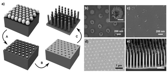
Yeom et al. report the use of nanosphere lithography for the fabrication of Si NWs through MACE as visible in [
126]. In particular, in a the schematic of the nanosphere lithography for the realization of the Ti/Au metal film used as a catalyst is shown. After the reduction of the nanosphere dimension by RIE a Ti adhesion layer of a few nm was deposited and then followed by 10–25 nm of Au deposition. In b–d, the main possible issues related to the nanosphere etching by RIE are reported. b shows that a continuous RIE reduction can increase the roughness of the nanospheres or it can ruin the starting spherical shape (c). Another issue is the formation of a continuous metal film (d) that completely covers the nanosphere, making the lift-off process very difficult. Finally, in e the authors show that as a function of the etching solution main parameters is possible to obtain tapered and porous Si NWs.
Figure 7. (
a) Scheme of the Si NWs fabrication by nanosphere lithography coupled with MACE. In particular: (A) nanosphere reduction, (B) lift-off process, and (C) metal-assisted chemical etching. SEM images of the main issues and challenging steps of the process: (
b) roughened nanosphere due to the RIE etching, in the inset a single roughened nanosphere is shown with a scale bar of 100 nm; (
c) nanosphere shape ruined after excessive RIE, (
d) unsuccessfully lift-off of an Au layer, (
e) tapered and porous Si NWs by MACE [
126]. This figure [
126] is reproduced with permission, Copyright 2013, John Wiley and Sons.
Several types of masking procedures are being used during these years besides the elicited EBL. Wendisch et al. report on the use of colloidal lithography followed by a plasma treatment to reduce the nanosphere size [
127]. Kim et al. [
113] demonstrate the use of an anodic aluminium oxide mask also used in several other works [
128,
129]. Other types of diffused masking procedures are polystyrene spheres [
112], laser interference lithography [
130], superionic solid state stamping [
119], and block copolymer lithography [
79,
131], and even Focused-Ion Beam (FIB) [
104].
Despite masked approaches permits to achieve a high control on the Si structure geometry, quantum confined Si NWs remain very complicated to be obtained due to the required resolution of few nanometers. Different authors [
12,
102] demonstrate the application of MACE without masking approaches. To surpass the common diameter limitations, the group of Irrera engineered a metal film approach by using few nanometers of Au or Ag discontinuous layers. By the percolative self-assembly of the gold obtained at the right deposition condition, this method permits to obtain Si NWs with an average diameter of few nanometers and with a very high density. In this case, no masking procedures are applied and the NWs geometry is determined by the negative development of the percolative gold geometry.
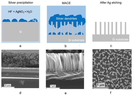
As shown in a–d, a discontinuous thin metal film is deposited by EBE on an oxide-free Si substrate (a,b). The sample is then immersed into a watery solution of H
2O
2:HF (around 0.44 M:5 M) with the metal that drives the Si oxidation and so the etching by the HF (c). Silicon nanowires are realized on the uncovered region, and the gold is finally removed by a gold etchant solution (d). All the processes are performed at room temperature. The presence of the gold is not attested inside the Si NWs by using Energy Dispersive X-ray analysis and Rutherford Backscattering Spectrometry [
132,
133].
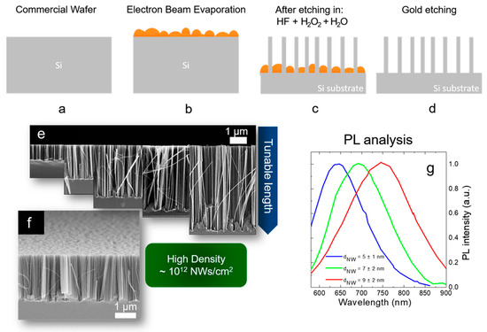
Figure 8. Scheme of Si NW synthesis by thin film MACE: (
a) native oxide etching, (
b) thin metal film deposition by EBE, (
c) metal-assisted chemical etching, (
d) gold etching. All the processes are performed at room temperature. (
e) Cross-section SEM images showing the possibility to tune the NW lengths from hundreds of nanometers to several micrometers. (
f) Tilted Cross-section SEM showing the high NW density of about 10
12 NWs/cm
2. Raman analysis of the first order stokes silicon peak. The average Si NW diameter is obtained for each different metal by fitting the Raman peak with the Campbell-Fauchet model [
134]. (
g) Normalized PL spectra of the different NW samples.
As shown in e, by changing the etching time the Si NW length varies from a few hundreds of nanometers to several micrometers. Therefore, as visible in f the density of the Si NWs is huge (about 10
12 NWs/cm
2) and this is a crucial point for all the applications. NW walls are smooth and with high crystalline quality, as previously observed by TEM [
132]. The average diameter of these synthesized Si NWs is determined by the thickness and the type of metal used as a catalyst. In fact, the thin metal layer is discontinuous and nanometric areas of uncovered silicon are present. The average dimension of these areas is determined by the material wettability and thickness. By using 10 nm of Ag, 2 nm of Au, and 3 nm of Au an average uncovered Si diameter of 12 nm, 9 nm, and 7 nm, was respectively demonstrated. These data were obtained from the statistical analysis performed on the SEM characterizations of the different films. The dimension of the diameters of these uncovered Si holes is strictly related to the final Si NW average diameters.
In particular, for the different metal thin films, the Si NW average diameters were obtained through Raman analyses. Indeed, the Raman signals of the Si are asymmetrical due to the quantum confinement effect, and fitting them with the Campbell-Fauchet method [
134] is possible to obtain the average NW diameter for each used metal. Average diameters of 10 nm, 7 nm, and 5 nm were obtained by using 10 nm of Ag (red line), 2 nm of Au (blue line), and 3 nm of Au (green line), respectively. These diameters were further confirmed by an accurate statistical TEM analysis. These NW diameters are enough to present quantum confinement effect. The emission of all the samples is reported in g, demonstrating their quantum confinement nature. In fact, the PL is redshifted by increasing the average diameter of the Si NWs, in perfect agreement with quantum confinement theory [
72,
135].
A possible drawback for this MACE approach is the lack of order. However, the desired geometry that can be obtained by a masking procedure. However, this thin metal film approach is cost-effective to obtain vertically aligned and room temperature luminescent Si NWs.
Different metals were employed in these years as a catalyst during a MACE approach such as Ag [
113,
132,
136,
137], Au [
64,
72,
102,
115], Pt [
104], Ni [
103], Cu [
123], W [
102]. The most used one remains the gold due to the best quality of fabricated Si NWs, for the stability in the etching solution compared to the silver, and for the fast and high tunable etching rate compared to other metals. Ti and other material such as AZO were also used as an adhesion layer for thick Au films, permitting to improve the film stability [
126,
127,
138]. Kim et al. report the application of an Au/Ag bilayer mesh to avoid the issue on the Ag stability and anodic dissolution during the etching [
113]. Wendisch et al. used an AZO reporting an improvement in the homogeneity of the etching and the possibility to vary the etching rate by changing its thickness [
127]. The same group and also Yeom et al. [
126] report gold delamination for high H
2O
2 concentrations (e.g., for 10:1:10 HF/H
2O
2/H2O) and for in general high etch rates (>400–600 nm/m) and small thin films (<20 nm) [
127]. The dependence on the etching rate is confirmed by other works [
64] and it is reasonable to assume that metal instability may be also affected by the wafer pre-treatment and deposition type. The etching rate is the key parameter, and a too fast process can be unstable and not affordable in terms of reproducibility. Indeed, in our experiment using few nanometers of Au we never observed gold delamination or large area defects in the Si NW array by an etching rate of 460 nm/min and a solution of HF (5 M) and H
2O
2 (0.44 M). The role of a high concentration of H
2O
2 is clear because it can increase the hole injection and reaction at the metal silicon interface, thus increasing the bubble formation during the etching possibly affecting the metal stability. These effects and issues regard the use of a connected Au film.
The etching rate is influenced by the gold coverage and so by the NWs diameter. Indeed, the amount of silicon to be etched depends on the covered region of the gold template, on the pitches (average gold region between Si NWs), and on the diameter of Si NWs [
127].
NW average diameter is determined by the metal film and usually ranges around 50 nm [
102,
113] but as seen in with the possibility to reach few nanometers and quantum confinement suitable dimensions [
12].
The reported preferential etching direction depends on several factors as wafer crystalline orientation, used etchant/oxidant solution, and its molar ratio, temperature, and metal film type and thickness [
102,
120,
122,
127,
139]. The wafer crystalline orientation has been found as the main parameter that determines the etching orientation with a preferential etching along the <100> direction [
90,
95,
102,
140,
141]. However, the concentration and ratio between the etchant and oxidant (usually HF/H
2O
2) can lead to other orientation etching. This can be understood considering that for a starting crystalline orientation, the etching orientation is driven by the reaction kinetic. Starting from Si (100) it was demonstrated that <100> remain the etching direction at a low etching rate [
113]. On the contrary, increasing the etching rate the same authors observed an etching in the <110> direction. The etching rate is characterized by the interplay of holes injection into silicon that is proportional to the metal electronegativity and to the oxidant H
2O
2 concentration and by the HF etching of silicon associated with the cleavage of Si back bonds [
113]. Indeed, Si atom density exposed to the interface depends on the considered crystal plane [
142]. At standard operation conditions, the hole injection is the limiting process of MACE. Increasing the concentration of injected holes above a certain threshold will cause the remotion of Si atoms where there is a higher concentration of Si back bonds causing in certain cases a change in the etching orientation. However, this condition requires a high enough HF concentration and the oxidant concentration as a limiting condition. Otherwise, with a Si (100) wafer, a low concentration of HF slowly etch the silicon in the <100> direction and the excess of holes diffuses causing new pore nucleation sites in presence of defect or doping atoms [
102,
113]. The temperature plays a role in the activation of non-<100> direction etching. Indeed, considering the same etching solution this can lead to an <100> etching at room temperature and <110> etching at higher temperatures (>50 °C for H
2O
2 1 M and HF/H
2O
2 molar ratio of about 23) [
113]. Temperature control is also used to low the etching rate and so the possible lateral etching with some works that report on cold MACE synthesis performed near 0 °C [
64], while other works used higher temperature above 55 °C to form zigzag Si NWs [
122].
As elicited, the type of metal mesh plays a role in the etching direction. Several experiments were performed in the same etching condition by using isolated metal particles instead of connected metal films. For metal film the etching is preferentially vertical to the wafer surface due to the difficulty of horizontal movement of the film. On the contrary, metal particles or isolated islands have more degrees of freedom. Indeed, MACE has been used to realize 3D etching taking advantage of the unconstrained metal particles movement during etching at the right conditions [
143,
144].
Lateral etching or in general a more isotropic etching is found to happen when a large number of holes are injected at the metal-silicon interface [
115,
145]. The diffusion of these holes can oxidize the sidewall, and lead to a lateral etching and porous nanostructures. The porosity of Si NWs depends on the doping level of Si wafer and on the solution concentration, especially of H
2O
2 or other oxidant agents [
102]. Heavily doped Si wafers produce more easily porous Si NWs because the doping atoms may act as nucleation centers (e.g., metal atoms in solution), catalyzing the lateral etching and the pore formations [
146,
147,
148]. In highly doped substrates, a competition between vertical etching and lateral etching (and so porous formation) occurs [
73,
149]. If the vertical etching is fast enough it is possible to obtain crystalline Si NWs at the right bath condition without the formation of porous structure [
102,
132]. As for the crystalline orientation, there is a strong dependence on the ratio between the H
2O
2 (and so hole injection) and HF (and so Si atom remotion) [
102].
Concerning the standard HF/H
2O
2 Mace bath Kim et al. reported that ethanol can be used to lower the etching rate influencing the etching direction and the final morphology [
150]. This can also lead to tapered Si NWs as demonstrate by Azeredo et al. by controlling the ethanol concentration [
151]. The addition of other oxidant co-solvent as methanol, isopropanol, acetonitrile, and so on has also been found as a method to change the etching orientation [
150].
A final consideration is the possible agglomeration of the NWs tips as a result of a very high aspect ratio, and as a function of the drying protocol. Several works reported on the NW tips bunching for very long Si NWs [
64,
92]. A possible solution proposed in these years is a drying protocol that involves a final bath in isopropanol (lower capillary forces than water) followed by natural evaporation of the alcohol [
64,
152]. Bunching of micro and nanostructures are typical issues of MEMS. Hence another viable industrial solution for Si NWs or other microstructures is to use a critical point dryer [
79,
153].
Metal film MACE permits a high flexibility of use for Si NW fabrication with several routes that can be followed to change diameter, orientation, density, porous formation, and so on. As demonstrated by the current trend of publications, the MACE method is becoming an outstanding tool for Si NWs synthesis and, for certain applications able to challenge RIE approaches for Si microstructure fabrication. In the next future, this relative novel approach may be really adopted for large-scale production of Si NWs thanks to the advantage of being compatible with the current industrial standard equipment. Indeed, the low-cost of this approach coupled with the very high aspect ratio makes it really appealing for microfabrication, challenging the more diffuse and consolidated approaches as DRIE.