Silicon is the undisputed leader for microelectronics among all the industrial materials and Si nanostructures flourish as natural candidates for tomorrow’s technologies due to the rising of novel physical properties at the nanoscale. In particular, silicon nanowires (Si NWs) are emerging as a promising resource in different fields such as electronics, photovoltaic, photonics, and sensing. Despite the plethora of techniques available for the synthesis of Si NWs, metal-assisted chemical etching (MACE) is today a cutting-edge technology for cost-effective Si nanomaterial fabrication already adopted in several research labs. During these years, MACE demonstrates interesting results for Si NW fabrication outstanding other methods. A critical study of all the main MACE routes for Si NWs is here presented, providing the comparison among all the advantages and drawbacks for different MACE approaches. All these fabrication techniques are investigated in terms of equipment, cost, complexity of the process, repeatability, also analyzing the possibility of a commercial transfer of these technologies for microelectronics, and which one may be preferred as industrial approach.
1. Introduction
In the last half-century, microelectronics and telecommunications have completely changed our world. The two application fields have in common the use of silicon (and silicon oxide) technology for both integrated circuits and optical fibers. The huge abundance on earth combined with its low-cost and its good electrical properties made the Si extremely advantageous compared to other semiconductors. Moreover, the stability, the easy and finely controlled realization of silicon oxide have determined the arising of Si as the leading material of the current technology, even outstanding germanium. Since 1970, we saw the doubling of Si transistors inside the same integrated circuit area approximately every 2 years. This technological trend was discovered by Moore, and is known as Moore’s law [1][2][3]. However, the trend has started to change in the last decades, reaching the saturation regime due to the complexity of a further down-scaling.
In the last half-century, microelectronics and telecommunications have completely changed our world. The two application fields have in common the use of silicon (and silicon oxide) technology for both integrated circuits and optical fibers. The huge abundance on earth combined with its low-cost and its good electrical properties made the Si extremely advantageous compared to other semiconductors. Moreover, the stability, the easy and finely controlled realization of silicon oxide have determined the arising of Si as the leading material of the current technology, even outstanding germanium. Since 1970, we saw the doubling of Si transistors inside the same integrated circuit area approximately every 2 years. This technological trend was discovered by Moore, and is known as Moore’s law [1,2,3]. However, the trend has started to change in the last decades, reaching the saturation regime due to the complexity of a further down-scaling.
Nowadays, one of the strictest limits is represented by the interconnection bottleneck. The dimension decrease implies longer and so, more power- and time-consuming interconnections, in addition to a more complex circuit realization [4]. The interconnection bottleneck due to RC delays limits the advantages of device downsizing, hindering their further downscaling. These issues are not the concern of a future challenge but are already present today.
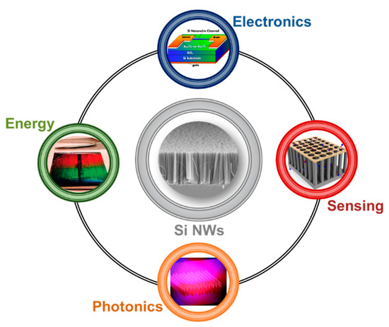
The arising of new physical phenomena on the nanoscale promoted the emerging of Si nanostructures for the past, present and future technologies. In particular, silicon nanowires (Si NWs) developed as a novel resource in many different fields, such as electronics [5][6][7], photovoltaics [8][9][10], photonics [11][12][13], and sensing [14][15][16], as schematized in
The arising of new physical phenomena on the nanoscale promoted the emerging of Si nanostructures for the past, present and future technologies. In particular, silicon nanowires (Si NWs) developed as a novel resource in many different fields, such as electronics [5,6,7], photovoltaics [8,9,10], photonics [11,12,13], and sensing [14,15,16], as schematized in .
Figure 1. Schematic showing the main application fields of silicon nanowire from the top corner to the left one in clockwise order: Electronics with a Si NW Field-Effect Transistor [7], Sensing with a Si NWs-based gas sensor [16], Photonics with Si NW luminescence [11], Energy with a solar cell based on a vertically-aligned Si NWs array [8]. Top [7] and right [16] images are reproduced with permission, Copyright 2005 and 2011, IOP Publishing. Bottom [11] and left [8] images are reproduced with permission, Copyright 2010, American Chemical Society.
Schematic showing the main application fields of silicon nanowire from the top corner to the left one in clockwise order: Electronics with a Si NW Field-Effect Transistor [7], Sensing with a Si NWs-based gas sensor [16], Photonics with Si NW luminescence [11], Energy with a solar cell based on a vertically-aligned Si NWs array [8]. Top [7] and right [16] images are reproduced with permission, Copyright 2005 and 2011, IOP Publishing. Bottom [11] and left [8] images are reproduced with permission, Copyright 2010, American Chemical Society.
Indeed, 1D nanostructures can be easily integrated in the typical flat architectures of integrated circuits, benefitting from such nanomaterials’ advantages.
During these years, a lot of effort was spent on the realization of novel Field Effect Transistor (FET) based on Si NWs [17][18][19], as well as on the integration of silicon photonics in microelectronics industries [11][20][21]. Metal Oxide Semiconductors Field Effect Transistor (MOSFET) technology’s constant miniaturization for microelectronics led scientists to design new improvements based on nanomaterials, such as nanowires and nanotubes. Si NWs arise as a natural candidate, and Lieber’s group [5] showed their substantial advantages on the state-of-the-art of planar silicon FET transistors. Their Si NW FET was obtained using the same planar geometry on a silicon bridge between the source and the drain. The FET was realized with p-type Si NWs having diameters of 10–20 nm dispersed on a 600 nm silicon oxide layer on top of a silicon wafer. Moreover, the paper of Feng et al. [6] reports a low-frequency noise behavior of Si NW FET compared to the planar standard due to the electrons quantum confinement in 1D. As an example of a typical Si NW FET architecture, the device obtained from Koo et al. [7] is shown at the top of
During these years, a lot of effort was spent on the realization of novel Field Effect Transistor (FET) based on Si NWs [17,18,19], as well as on the integration of silicon photonics in microelectronics industries [11,20,21]. Metal Oxide Semiconductors Field Effect Transistor (MOSFET) technology’s constant miniaturization for microelectronics led scientists to design new improvements based on nanomaterials, such as nanowires and nanotubes. Si NWs arise as a natural candidate, and Lieber’s group [5] showed their substantial advantages on the state-of-the-art of planar silicon FET transistors. Their Si NW FET was obtained using the same planar geometry on a silicon bridge between the source and the drain. The FET was realized with p-type Si NWs having diameters of 10–20 nm dispersed on a 600 nm silicon oxide layer on top of a silicon wafer. Moreover, the paper of Feng et al. [6] reports a low-frequency noise behavior of Si NW FET compared to the planar standard due to the electrons quantum confinement in 1D. As an example of a typical Si NW FET architecture, the device obtained from Koo et al. [7] is shown at the top of .
2. Silver Salt and Single Step MACE
In 2002 Peng et al. realized a high density of vertically aligned Si NWs with the MACE by using an AgNO3:HF aqueous solution in a teflon-lined stainless-steel autoclave [22]. After three cleaning steps in acetone, ethanol, and diluted aqueous HF solution to remove organic grease and native oxide, the cleaned wafer was etched with 5.0:0.02 M solution of HF:AgNO
:HF aqueous solution in a teflon-lined stainless-steel autoclave [75]. After three cleaning steps in acetone, ethanol, and diluted aqueous HF solution to remove organic grease and native oxide, the cleaned wafer was etched with 5.0:0.02 M solution of HF:AgNO3
and treated at 50 °C for 60 min. During the etching process, the silicon wafers showed the formation of a thick layer of Ag dendrites on top of the nanowires, which is promptly removed by nitric acid solution (70%). Indeed, due to the formation of silver precipitates and to the use of AgNO3
, this method is commonly known as the silver salts approach and it is identified as the main single step MACE approach.
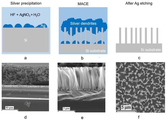
In a–d the scheme of the silver salt process is shown in detail. After the cleaning procedure, the sample is immersed in an aqueous AgNO3
:HF solution (a). When in solution, the AgNO3
catalyst precipitates forming Ag nanoparticles (NPs) which are randomly distributed onto the silicon flat surface, catalyzing the HF driven Si etching in a very similar way to the one described for H2
O2
. Indeed, AgNO3
acts both as an oxidant and as a metal source. Ag NPs, with dimensions and density related to the starting silver nitrate solution, precipitate onto the Si surface biasing the etching. The Ag nanoparticles formed in solution are more electronegative than the Si and inject holes into the substrate that is oxidized due to the presence of radical NO−3
. The selective oxidation process is driven at the Ag NPs/Si interface resulting in the formation of SiO2
underneath the metal NPs, and the etching continues by the HF presence, resulting in the formation of Si nanowires in the Si uncovered regions. As a byproduct of the process, Ag dendrites are formed onto the newly etched Si NWs as depicted in the scheme in b. The Ag dendrites form a dense network of several microns thick (about 40 µm) onto the Si NWs, as displayed in the SEM cross-section (d). Finally, the silver dendrites in excess are selectively etched by nitric acid (c) and the Si NWs vertical array are obtained as shown from the SEM cross-section (e).
Figure 5.
Scheme of Si NWs synthesis by silver salt single step MACE: (
a
) Ag precipitation from the HF/AgNO3 solution onto the Si surface, (
b
) Ag dendrites and Si NW formation, (
c
) Ag dendrites removal by nitric acid. Cross-section SEM of Si NW realized onto p-type (111) by HF/AgNO
3
single step MACE for 30 min, (
d
) during Ag dendrites formation, and (
e) after its removal [23]. (
) after its removal [76]. ( f
) SEM plan view of Si NWs produced by HF/KAuCl
4 synthesis after 30 s [24]. (
synthesis after 30 s [80]. ( d
,
e) ref. [23] are reproduced with permission, Copyright 2006, John Wiley and Sons. (
) ref. [76] are reproduced with permission, Copyright 2006, John Wiley and Sons. ( f) ref. [24] is reproduced with permission, Copyright 2005, John Wiley and Sons.
) ref. [80] is reproduced with permission, Copyright 2005, John Wiley and Sons.
e shows the typical cross-section of Si NWs realized by using a HF/AgNO3 solution for 30 min with concentrations of 4.6/0.02 M. The Si NWs were obtained onto a (111) p-Si substrate preserving their crystalline quality, and are about 4 µm long [23]. The average diameter of NWs realized by single step approaches is about 70 nm ± 20 nm [25] as usually obtained by the silver salt approach, ranging from about 60 nm up to 140 nm on average [26]. As already stated, the length of the NW array can be increased with the etching time from a few hundreds of nm up to several tens of microns, leading to nanostructures with an aspect ratio above 200 [27]. Aside from AgNO
solution for 30 min with concentrations of 4.6/0.02 M. The Si NWs were obtained onto a (111) p-Si substrate preserving their crystalline quality, and are about 4 µm long [76]. The average diameter of NWs realized by single step approaches is about 70 nm ± 20 nm [77] as usually obtained by the silver salt approach, ranging from about 60 nm up to 140 nm on average [78]. As already stated, the length of the NW array can be increased with the etching time from a few hundreds of nm up to several tens of microns, leading to nanostructures with an aspect ratio above 200 [79]. Aside from AgNO3
precursors, also KAuCl4
is widely diffused for the single step MACE process. The SEM plan-view of Si NWs obtained by MACE with HF/KAuCl4
with concentrations ratio of 6.0/0.005 M after 30s, as shown in f [24].
f [80].
This single step silver salts MACE process is fast, does not need complicated sample preparation, and is less expensive than the other MACE procedures. In their pioneering works, Peng et al. investigated the strong correlation of the growth parameters, mainly the solution type and concentration, growth temperature, illumination, and substrate orientation.
Indeed, a variety of oxidative metal-based solutions can be used to drive the Si etching, such as AgNO3 [28][29], KAuCl
[81,82], KAuCl4 [24], Fe(NO
[80], Fe(NO3
)3 [30], KMnO
[83], KMnO4 [31], KBrO
[84], KBrO3 [32], K2Cr
[85], K2Cr2
O7 [31], and so on, however Ag and Fe-based oxidants presents the lowest redox potential [33]. Additionally, different noble metals such as Ag, Pt, Fe, Pd, and Au are mainly used to catalytically reduce H
[84], and so on, however Ag and Fe-based oxidants presents the lowest redox potential [70]. Additionally, different noble metals such as Ag, Pt, Fe, Pd, and Au are mainly used to catalytically reduce H2
O and O2 [34][35][36]. In general, dendrite structures are produced during the oxidation and dissolution of the Si substrate when the metal ions are reduced to particles, resulting in the formation of vertically aligned Si NWs with differences in the oxidation and etching rate, and for the NW morphology [33]. Higher concentrations of the metal salts result in a denser metal catalyst, hence forming nanowires with lower density, smaller diameter, and more spaced within each other. Indeed, it is not simple to control the NW planar arrangement by this approach, since their diameter, density, and interspacing are determined by the metal concentration.
[86,87,88]. In general, dendrite structures are produced during the oxidation and dissolution of the Si substrate when the metal ions are reduced to particles, resulting in the formation of vertically aligned Si NWs with differences in the oxidation and etching rate, and for the NW morphology [70]. Higher concentrations of the metal salts result in a denser metal catalyst, hence forming nanowires with lower density, smaller diameter, and more spaced within each other. Indeed, it is not simple to control the NW planar arrangement by this approach, since their diameter, density, and interspacing are determined by the metal concentration.
Another parameter highly affecting the morphologies of the etched NWs is the type of noble metal used during the MACE. Usually, Ag and Au nanoparticles formed in solution result in straight pores during the etching, while straight or helical pores can be achieved by Pt catalyst were reported by Tsujino et al. [37][38]. Indeed, through its precipitation, Pt nanoparticles move randomly during the etching, resulting in curvy pores without a uniform etching direction. Moreover, the formation of porous nanostructures is also influenced by metal. Generally, Au-coated or Ag-coated substrates result in smoother NWs with low porosity, while Pt-driven synthesis results in a more porous structure [37]. Similarly, while standard p and n doping results in a similar etching rate for the formation of low porosity NWs, the presence of a high concentration of dopants (around 10
Another parameter highly affecting the morphologies of the etched NWs is the type of noble metal used during the MACE. Usually, Ag and Au nanoparticles formed in solution result in straight pores during the etching, while straight or helical pores can be achieved by Pt catalyst were reported by Tsujino et al. [89,90]. Indeed, through its precipitation, Pt nanoparticles move randomly during the etching, resulting in curvy pores without a uniform etching direction. Moreover, the formation of porous nanostructures is also influenced by metal. Generally, Au-coated or Ag-coated substrates result in smoother NWs with low porosity, while Pt-driven synthesis results in a more porous structure [89]. Similarly, while standard p and n doping results in a similar etching rate for the formation of low porosity NWs, the presence of a high concentration of dopants (around 1020
dopant atoms × cm−3
) for p++ and n++ Si wafers results in the formation of highly porous Si NWs due to the occurrence of lateral etching.
Peng’s MACE synthesis is a single step approach for the easy and fast formation of Si nanowires without the need of a second etching step in other oxidizing species such as H2
O2 [39] or thin film depositions [40].
[91] or thin film depositions [92].
In general, this process is carried out at room temperature although the correlation between the temperature and the etching rate structure was also studied. The NW length approximately follows a linear trend with time. However, the etching rate also depends on the temperature and increases linearly between 0° to 50 °C [41]. Another parameter affecting the etching rate is illumination. If the intensity of illumination is sufficiently high so that the injection of the photoexcited holes is comparable or higher than the concentration of holes injected from the oxidant species, then the etching occurs faster. Studies revealed that the process is independent of the room illumination within a confidence of 5%, but an increment of about 1.5 times the etching rate was observed under light illumination with a 20 W lamp [42].
In general, this process is carried out at room temperature although the correlation between the temperature and the etching rate structure was also studied. The NW length approximately follows a linear trend with time. However, the etching rate also depends on the temperature and increases linearly between 0° to 50 °C [93]. Another parameter affecting the etching rate is illumination. If the intensity of illumination is sufficiently high so that the injection of the photoexcited holes is comparable or higher than the concentration of holes injected from the oxidant species, then the etching occurs faster. Studies revealed that the process is independent of the room illumination within a confidence of 5%, but an increment of about 1.5 times the etching rate was observed under light illumination with a 20 W lamp [94].
To control the axial orientation of vertically aligned Si nanowires it is possible to vary the Si wafers with other orientations, such as (100) and (110). According to the back-bond breaking theory [43][44], the (100)-orientation presents the lowest bond energy and so (100) wafer are preferentially etched vertically along with this orientation. In contrast, an atom on the (110) and (111) have three back-bond to break, hence the etching occurs again preferentially along the (100) when the etching rate dominates on the oxidation process. On the contrary, increasing the oxidant concentration favors the etching of non-(100) orientation resulting in tilted nanowires [45][46][47].
To control the axial orientation of vertically aligned Si nanowires it is possible to vary the Si wafers with other orientations, such as (100) and (110). According to the back-bond breaking theory [95,96], the (100)-orientation presents the lowest bond energy and so (100) wafer are preferentially etched vertically along with this orientation. In contrast, an atom on the (110) and (111) have three back-bond to break, hence the etching occurs again preferentially along the (100) when the etching rate dominates on the oxidation process. On the contrary, increasing the oxidant concentration favors the etching of non-(100) orientation resulting in tilted nanowires [97,98,99].
However, a crucial drawback compared to the other MACE approaches is that during the process the presence of Ag dendrites is attested onto the samples and the dendrites etching may damage the Si NWs, resulting also in Ag contaminants [48]. Hence, the MACE single step methods allow to achieve high yield, fast production rate at the expense of a lack of control on the NWs planar arrangement and diameter control [23].
However, a crucial drawback compared to the other MACE approaches is that during the process the presence of Ag dendrites is attested onto the samples and the dendrites etching may damage the Si NWs, resulting also in Ag contaminants [100]. Hence, the MACE single step methods allow to achieve high yield, fast production rate at the expense of a lack of control on the NWs planar arrangement and diameter control [76].
Indeed, more advanced syntheses were optimized by using masked approaches, granting also the control on the NWs diameter and planar arrangement (density and spacing) by using single-step MACE coupled with lithography processes.
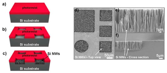
As an example, Nassiopoulou et al. used UV photolithography onto p-type (100) Si wafers with resistivity ranging of about 1 Ω × cm to open square-shaped windows ranging from 2 × 2 μm2
to 400 × 400 μm2
with the AZ5214 photoresist applied by spin coating, as shown in a,b. Then, Si NWs were grown by MACE in a AgNO3
/HF/H2
O solution with a concentration ratio of 0.67 g:35 mL:182 mL at a temperature of 30 °C, as reported in c. d shows the top-view SEM microscopies imaged of the exposed windows where Si NWs are grown, confirming the efficiency of this approach. The SEM cross-section reported in e,f shows that it is possible to grown 15 µm long vertically aligned Si NWs with good quality even at the window edge, confirming the robustness of two-steps MACE methods. Nonetheless, photolithography is limited to small areas of about 104
µm2 [49], and other approaches based on two step MACE using films achieved by the metal deposition onto silica bead can also be used [50].
[67], and other approaches based on two step MACE using films achieved by the metal deposition onto silica bead can also be used [101].
Figure 6.
Flow chart for Si NW formation by MACE at a temperature of 30 °C on the confined areas by (
a
) applying AZ5214 photoresist, (
b
) opening windows from 2 × 2 μm
2
to 400 × 400 μm
2
, and using (
c
) AgNO
3
/HF/H
2
O solution with a concentration ratio of 0.67 g:35 mL:182 mL. (
d
) Plan-view and (
e
,
f) Cross-sections SEM images of the etched confined areas [49]. This figure [49] is reproduced with permission (open access), Copyright 2011, Springer Nature.
) Cross-sections SEM images of the etched confined areas [67]. This figure [67] is reproduced with permission (open access), Copyright 2011, Springer Nature.
The primary catalysts for MACE are Ag, Au, and Pt because of their stability and catalytic activity in HF/ H2
O2 solution, but apart from their high cost, the main drawbacks of these noble metals are their diffusivity in Si, which is detrimental to the performance of CMOS [51]. As an alternative W and Ni can also be used. Both W/H
solution, but apart from their high cost, the main drawbacks of these noble metals are their diffusivity in Si, which is detrimental to the performance of CMOS [102]. As an alternative W and Ni can also be used. Both W/H2
O2
and Ni/H2
O2 result in a lower etching rate compared to noble metal, the first one allowing the production of very large holes up to 800 nm in diameter and the latter resulting in the formation of pyramidal etched structures [52].
result in a lower etching rate compared to noble metal, the first one allowing the production of very large holes up to 800 nm in diameter and the latter resulting in the formation of pyramidal etched structures [103].
Gallium and Platinum ions deposited by focused ion beam can also be adopted for the Si MACE [53] and the produced NWs show poor morphology and low reproducibility.
Gallium and Platinum ions deposited by focused ion beam can also be adopted for the Si MACE [104] and the produced NWs show poor morphology and low reproducibility.
Ti metal was also introduced to HF/ H2
O2 aqueous etchant to etch Ag-loaded Si (n-type, 100) [54], resulting in a lower etching rate by increasing Ti concentration. This decrease was attributed to the lowering of H
aqueous etchant to etch Ag-loaded Si (n-type, 100) [105], resulting in a lower etching rate by increasing Ti concentration. This decrease was attributed to the lowering of H2
O2
concentration because TiF62−
produced by the reaction of Ti and HF can complex with H2
O2
to form anions of [TiF6
(H2
O2
)]2−
.
Similar to AgNO3, also AgO (insoluble) [55] and Ag
, also AgO (insoluble) [106] and Ag2O (soluble) [56] have been utilized instead of AgNO
O (soluble) [107] have been utilized instead of AgNO3
in one-step MACE always forming Ag dendrites as a byproduct. The activation energy of Si etching for HF/AgO and HF/Ag2
O are lower smaller than HF/AgNO3, being 0.20 eV in HF/AgO etchant [55], and 0.15 eV in HF/Ag
, being 0.20 eV in HF/AgO etchant [106], and 0.15 eV in HF/Ag2O etchant [56].
O etchant [107].
The same MACE techniques used for Si NWs synthesis can also be used for the production of Si microstructures [57], and 3D structures [58].
The same MACE techniques used for Si NWs synthesis can also be used for the production of Si microstructures [108], and 3D structures [109].
Si microstructures are easily obtained in a sequence of steps that include selective MACE Si NWs in pre-patterned regions by masked photolithography, which are then sacrificed in an over-etching process leaving the microstructures standing. Si microstructures first synthesis step consists of the patterning realization on Si wafer by photolithography, deposition of noble metal catalyst for MACE in HF/oxidants solution to produce Si nanowires only in the patterned areas, and then etching away the Si nanowires in a KOH-based solution [59]. To allow the MACE processing, noble metal (mainly Ag, Au, and Pt) can be deposited onto the Si surface by different methods which include thermal evaporation [60][61], sputtering [47], electron beam evaporation [27], electroless deposition [24] and spin coating [62]. The whole process can be carried out at room temperature without complex equipment or special facilities, and it can be applicable on a wafer-scale.
Si microstructures are easily obtained in a sequence of steps that include selective MACE Si NWs in pre-patterned regions by masked photolithography, which are then sacrificed in an over-etching process leaving the microstructures standing. Si microstructures first synthesis step consists of the patterning realization on Si wafer by photolithography, deposition of noble metal catalyst for MACE in HF/oxidants solution to produce Si nanowires only in the patterned areas, and then etching away the Si nanowires in a KOH-based solution [110]. To allow the MACE processing, noble metal (mainly Ag, Au, and Pt) can be deposited onto the Si surface by different methods which include thermal evaporation [111,112], sputtering [99], electron beam evaporation [79], electroless deposition [80] and spin coating [69]. The whole process can be carried out at room temperature without complex equipment or special facilities, and it can be applicable on a wafer-scale.
3. Metal Film or Two Step MACE
In the literature it is possible to find both the name of metal film
and thin film
approaches for several types of two step MACE routes. In this paragraph will be presented all the methods reporting the use of metal film in the literature.
Metal film can be deposited on Si wafer and used as a metal catalyst in a MACE approach. Several works report the use of metal film to offer several advantages in terms of geometry control, diameter, spacing, and density [27][47][61][63][64] compared to MACE approaches that involve layers of nanoparticles similarly to single step MACE (e.g., the silver salts). The metal geometry determines the formation of silicon nanostructures and self-assembly methods can also be used for masking. Most of the approaches take advantage of metal films integration with some masking methods to strictly determine the geometry of the metal array (negative mask of the silicon nanowire array). Indeed, to surpass the lack of control in the Si NWs array geometry, the MACE can be coupled with self-assembly or a lithography process by using ordered metal film as catalysts. This method can be used to realize several silicon nano- and microstructures with a very high aspect ratio, surpassing the limit of 50:1 typical of DRIE. Different groups [65][51] report the use of MACE by high control patterned metal films (usually obtained through EBL) for nano and microfabrication of silicon. This approach can be used to fabricate Si gratings [65], honeycomb array [66] and other microstructures [67][68] or vertical aligned [33][51][63][69], tilted [46][70][71][72], zigzag [73][74][75], or tapered Si nanowires [76].
Metal film can be deposited on Si wafer and used as a metal catalyst in a MACE approach. Several works report the use of metal film to offer several advantages in terms of geometry control, diameter, spacing, and density [79,99,112,113,114] compared to MACE approaches that involve layers of nanoparticles similarly to single step MACE (e.g., the silver salts). The metal geometry determines the formation of silicon nanostructures and self-assembly methods can also be used for masking. Most of the approaches take advantage of metal films integration with some masking methods to strictly determine the geometry of the metal array (negative mask of the silicon nanowire array). Indeed, to surpass the lack of control in the Si NWs array geometry, the MACE can be coupled with self-assembly or a lithography process by using ordered metal film as catalysts. This method can be used to realize several silicon nano- and microstructures with a very high aspect ratio, surpassing the limit of 50:1 typical of DRIE. Different groups [64,102] report the use of MACE by high control patterned metal films (usually obtained through EBL) for nano and microfabrication of silicon. This approach can be used to fabricate Si gratings [64], honeycomb array [115] and other microstructures [116,117] or vertical aligned [70,102,113,118], tilted [98,119,120,121], zigzag [122,123,124], or tapered Si nanowires [125].
A typical approach is the one of Miao et al. [66] used to realize a silicon honeycomb array. This array was obtained by depositing the metal in a previously patterned resist, in this case, exposed and developed by UV lithography. After the lift-off, the metal results structured as the negative of the resist mask. After a typical MACE process at room temperature in a HF/H
A typical approach is the one of Miao et al. [115] used to realize a silicon honeycomb array. This array was obtained by depositing the metal in a previously patterned resist, in this case, exposed and developed by UV lithography. After the lift-off, the metal results structured as the negative of the resist mask. After a typical MACE process at room temperature in a HF/H2
O2
bath (H2
O2 30 wt.%, HF 40wt.%), they obtained a honeycomb array of 50 µm width and 280 µm deep [66].
30 wt.%, HF 40wt.%), they obtained a honeycomb array of 50 µm width and 280 µm deep [115].
Another possible approach reported by Li et al. [65] consists of patterning the metal (Ti-Au) through an RIE process. Initially, a 3 nm of Ti as an adhesion layer and 20 nm of Au is deposited by EBE in a Si substrate. The sample is then spun with PMMA and patterned through EBL. The pattern realized through EBL corresponds to the final structure. In fact, the exposed metal is then etched by RIE and then the PMMA is removed. Finally, the sample is immersed in a H
Another possible approach reported by Li et al. [64] consists of patterning the metal (Ti-Au) through an RIE process. Initially, a 3 nm of Ti as an adhesion layer and 20 nm of Au is deposited by EBE in a Si substrate. The sample is then spun with PMMA and patterned through EBL. The pattern realized through EBL corresponds to the final structure. In fact, the exposed metal is then etched by RIE and then the PMMA is removed. Finally, the sample is immersed in a H2
O2
:HF solution with the hydrogen peroxide used as an oxidation agent and a high aspect ratio is obtained with Si structures characterized by a length of 250 nm and a height of 21 µm.
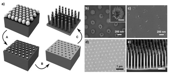
Yeom et al. report the use of nanosphere lithography for the fabrication of Si NWs through MACE as visible in [77]. In particular, in
[126]. In particular, in a the schematic of the nanosphere lithography for the realization of the Ti/Au metal film used as a catalyst is shown. After the reduction of the nanosphere dimension by RIE a Ti adhesion layer of a few nm was deposited and then followed by 10–25 nm of Au deposition. In b–d, the main possible issues related to the nanosphere etching by RIE are reported. b shows that a continuous RIE reduction can increase the roughness of the nanospheres or it can ruin the starting spherical shape (c). Another issue is the formation of a continuous metal film (d) that completely covers the nanosphere, making the lift-off process very difficult. Finally, in e the authors show that as a function of the etching solution main parameters is possible to obtain tapered and porous Si NWs.
Figure 7.
(
a
) Scheme of the Si NWs fabrication by nanosphere lithography coupled with MACE. In particular: (A) nanosphere reduction, (B) lift-off process, and (C) metal-assisted chemical etching. SEM images of the main issues and challenging steps of the process: (
b
) roughened nanosphere due to the RIE etching, in the inset a single roughened nanosphere is shown with a scale bar of 100 nm; (
c
) nanosphere shape ruined after excessive RIE, (
d
) unsuccessfully lift-off of an Au layer, (
e) tapered and porous Si NWs by MACE [77]. This figure [77] is reproduced with permission, Copyright 2013, John Wiley and Sons.
) tapered and porous Si NWs by MACE [126]. This figure [126] is reproduced with permission, Copyright 2013, John Wiley and Sons.
Several types of masking procedures are being used during these years besides the elicited EBL. Wendisch et al. report on the use of colloidal lithography followed by a plasma treatment to reduce the nanosphere size [78]. Kim et al. [63] demonstrate the use of an anodic aluminium oxide mask also used in several other works [79][80]. Other types of diffused masking procedures are polystyrene spheres [61], laser interference lithography [81], superionic solid state stamping [70], and block copolymer lithography [27][82], and even Focused-Ion Beam (FIB) [53].
Several types of masking procedures are being used during these years besides the elicited EBL. Wendisch et al. report on the use of colloidal lithography followed by a plasma treatment to reduce the nanosphere size [127]. Kim et al. [113] demonstrate the use of an anodic aluminium oxide mask also used in several other works [128,129]. Other types of diffused masking procedures are polystyrene spheres [112], laser interference lithography [130], superionic solid state stamping [119], and block copolymer lithography [79,131], and even Focused-Ion Beam (FIB) [104].
Despite masked approaches permits to achieve a high control on the Si structure geometry, quantum confined Si NWs remain very complicated to be obtained due to the required resolution of few nanometers. Different authors [12][51] demonstrate the application of MACE without masking approaches. To surpass the common diameter limitations, the group of Irrera engineered a metal film approach by using few nanometers of Au or Ag discontinuous layers. By the percolative self-assembly of the gold obtained at the right deposition condition, this method permits to obtain Si NWs with an average diameter of few nanometers and with a very high density. In this case, no masking procedures are applied and the NWs geometry is determined by the negative development of the percolative gold geometry.
Despite masked approaches permits to achieve a high control on the Si structure geometry, quantum confined Si NWs remain very complicated to be obtained due to the required resolution of few nanometers. Different authors [12,102] demonstrate the application of MACE without masking approaches. To surpass the common diameter limitations, the group of Irrera engineered a metal film approach by using few nanometers of Au or Ag discontinuous layers. By the percolative self-assembly of the gold obtained at the right deposition condition, this method permits to obtain Si NWs with an average diameter of few nanometers and with a very high density. In this case, no masking procedures are applied and the NWs geometry is determined by the negative development of the percolative gold geometry.
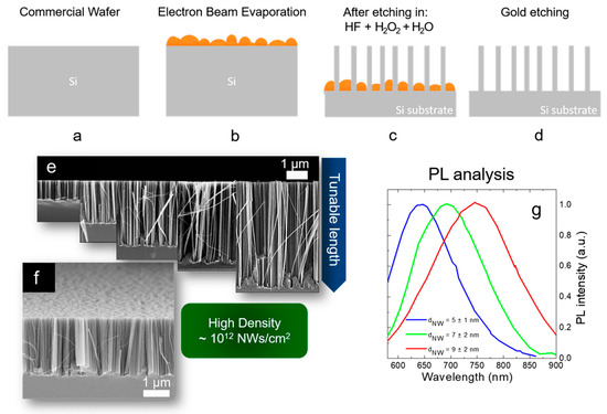
As shown in a–d, a discontinuous thin metal film is deposited by EBE on an oxide-free Si substrate (a,b). The sample is then immersed into a watery solution of H2
O2
:HF (around 0.44 M:5 M) with the metal that drives the Si oxidation and so the etching by the HF (c). Silicon nanowires are realized on the uncovered region, and the gold is finally removed by a gold etchant solution (d). All the processes are performed at room temperature. The presence of the gold is not attested inside the Si NWs by using Energy Dispersive X-ray analysis and Rutherford Backscattering Spectrometry [83][84].
d). All the processes are performed at room temperature. The presence of the gold is not attested inside the Si NWs by using Energy Dispersive X-ray analysis and Rutherford Backscattering Spectrometry [132,133].
Figure 8.
Scheme of Si NW synthesis by thin film MACE: (
a
) native oxide etching, (
b
) thin metal film deposition by EBE, (
c
) metal-assisted chemical etching, (
d
) gold etching. All the processes are performed at room temperature. (
e
) Cross-section SEM images showing the possibility to tune the NW lengths from hundreds of nanometers to several micrometers. (
f
) Tilted Cross-section SEM showing the high NW density of about 10
12
NWs/cm
2. Raman analysis of the first order stokes silicon peak. The average Si NW diameter is obtained for each different metal by fitting the Raman peak with the Campbell-Fauchet model [85]. (
. Raman analysis of the first order stokes silicon peak. The average Si NW diameter is obtained for each different metal by fitting the Raman peak with the Campbell-Fauchet model [134]. ( g
) Normalized PL spectra of the different NW samples.
As shown in e, by changing the etching time the Si NW length varies from a few hundreds of nanometers to several micrometers. Therefore, as visible in f the density of the Si NWs is huge (about 1012
NWs/cm2) and this is a crucial point for all the applications. NW walls are smooth and with high crystalline quality, as previously observed by TEM [84]. The average diameter of these synthesized Si NWs is determined by the thickness and the type of metal used as a catalyst. In fact, the thin metal layer is discontinuous and nanometric areas of uncovered silicon are present. The average dimension of these areas is determined by the material wettability and thickness. By using 10 nm of Ag, 2 nm of Au, and 3 nm of Au an average uncovered Si diameter of 12 nm, 9 nm, and 7 nm, was respectively demonstrated. These data were obtained from the statistical analysis performed on the SEM characterizations of the different films. The dimension of the diameters of these uncovered Si holes is strictly related to the final Si NW average diameters.
) and this is a crucial point for all the applications. NW walls are smooth and with high crystalline quality, as previously observed by TEM [132]. The average diameter of these synthesized Si NWs is determined by the thickness and the type of metal used as a catalyst. In fact, the thin metal layer is discontinuous and nanometric areas of uncovered silicon are present. The average dimension of these areas is determined by the material wettability and thickness. By using 10 nm of Ag, 2 nm of Au, and 3 nm of Au an average uncovered Si diameter of 12 nm, 9 nm, and 7 nm, was respectively demonstrated. These data were obtained from the statistical analysis performed on the SEM characterizations of the different films. The dimension of the diameters of these uncovered Si holes is strictly related to the final Si NW average diameters.
In particular, for the different metal thin films, the Si NW average diameters were obtained through Raman analyses. Indeed, the Raman signals of the Si are asymmetrical due to the quantum confinement effect, and fitting them with the Campbell-Fauchet method [85] is possible to obtain the average NW diameter for each used metal. Average diameters of 10 nm, 7 nm, and 5 nm were obtained by using 10 nm of Ag (red line), 2 nm of Au (blue line), and 3 nm of Au (green line), respectively. These diameters were further confirmed by an accurate statistical TEM analysis. These NW diameters are enough to present quantum confinement effect. The emission of all the samples is reported in
In particular, for the different metal thin films, the Si NW average diameters were obtained through Raman analyses. Indeed, the Raman signals of the Si are asymmetrical due to the quantum confinement effect, and fitting them with the Campbell-Fauchet method [134] is possible to obtain the average NW diameter for each used metal. Average diameters of 10 nm, 7 nm, and 5 nm were obtained by using 10 nm of Ag (red line), 2 nm of Au (blue line), and 3 nm of Au (green line), respectively. These diameters were further confirmed by an accurate statistical TEM analysis. These NW diameters are enough to present quantum confinement effect. The emission of all the samples is reported in g, demonstrating their quantum confinement nature. In fact, the PL is redshifted by increasing the average diameter of the Si NWs, in perfect agreement with quantum confinement theory