 +1 credit
| Version | Summary | Created by | Modification | Content Size | Created at | Operation |
|---|---|---|---|---|---|---|
| 1 | Zheng Gong | + 5521 word(s) | 5521 | 2021-04-22 05:42:45 | | | |
| 2 | Camila Xu | Meta information modification | 5521 | 2021-04-25 07:38:42 | | |
Video Upload Options
Layer transfer is a technique to transfer a layer of a particular semiconductor material, often of a wafer-scale size, from the original substrate to the target substrate of interest.
1. Layer Transfer Techniques
Layer transfer is a technique to transfer a layer of a particular semiconductor material, often of a wafer-scale size, from the original substrate to the target substrate of interest. The key process is to remove the growth substrate on which the semiconductor layer is deposited. The technique allows the integration of both lattice-matched and mismatched material systems for enabling extended functionality and performance by assembling diverse materials or devices in a more compact space. The additional benefit is the potential reuse of the growth substrate if it is not damaged during lift-off, thereby reducing the cost [1][2][3]. As one example, the transfer of GaN micro-LEDs onto silicon complementary metal oxide semiconductor (CMOS) allows a high-quality display with additional functionality such as pulse control.
The conventional method for layer transfer is mainly based on wafer bonding and mechanical thinning [4][5][6][7]. However, thinning techniques are difficult for accurate control of the film thickness and surface roughness across the wafer. For instance, in most cases, reducing the layer thickness down to 10 µm by mechanical thinning is extremely challenging. To address these challenges, a variety of new lift-off technologies have been developed to assist the wafer-scale layer transfer, some of which have the potential for volume production. These include epitaxial lift-off (ELO), mechanical spalling, laser lift-off, and ion cutting, as schematically shown in Figure 1 below.
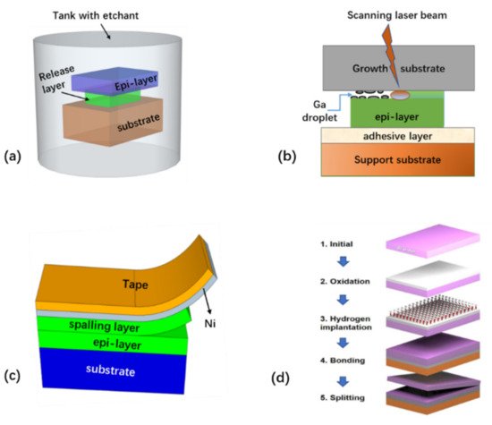
Figure 1. Sketches of common layer transfer techniques: (a) chemical epitaxial lift-off, (b) laser lift-off, (c) mechanical spalling, and (d) ion cutting.
2. Layer Transfer by Epitaxial Lift-off (ELO)
Referring to Figure 1a, ELO relies on the removal of a releasable or sacrificial layer introduced in the epi-stacks using various chemical etchants, such that the epi-layer on top of the releasing layer can be transferred to other substrates while preserving the original growth substrate [8][9][10][11][12][13][14][15][16][3][17][18][19][20][21][22][23][24][25][26][27][28][29][30][31][32][33][34][35][36][37][38][39][40][41][42][43][44][45][46][47][48][49][50][51][52][53][54][55][56][57][58][59][60][61][62][63][64][65]. The primary requirements for this technique are: (i) high etch selectivity of the releasing layer, (ii) the capability for high-quality growth of the epi-layer on the releasing layer, and (iii) minimized damage to the epi-layer after release. Therefore, the suitable release layer not only determines the epi-layer quality, but also determines the ELO quality. Selecting the right release layer is highly dependent on the epi-layer (to be released), substrate, and etchant solvent to be used. Commonly, chemical lift-off of small samples is relatively quick, but wafer-level release remains challenging. Depending on the specific release layer in the epi-stack, the etching duration for releasing the full wafer may vary from a few hours to a few days, which may impose practical limitations for large-volume production. Therefore, to accelerate the release, several variants of the conventional ELO have been proposed, including weight-assisted, surface tension force-assisted, or roller-assisted ELO techniques [3][51][52].
2.1. ELO Assisted by Lattice-Matched Release Layer
Earlier ELO studies of III-V semiconductor layers in the past were mainly based on lattice-matched release layers, primarily because the growth of high-quality layered semiconductors on a lattice-matched release layer is much easier than on a dissimilar sacrificial layer. Depending on the specific epitaxial structures and the growth substrate, the release layer and corresponding etching solvent can be quite different. For example, one common release layer for III-V semiconductors grown on GaAs is AlAs [55], which is a material lattice- matched with the substrate and can be removed by hydrofluoric acid. However, a recent investigation reveals that etching AlAs using hydrofluoric acid is fast, but it leads to reaction residuals and increased roughness of the released layer and substrate [3]. To alleviate this issue, lattice-matched AlInP was introduced to act as the release layer, which can be etched by a different solvent, hydrochloride acid [3]. In the latter case, very smooth III-V layers and substrate free from residuals can be achieved via a modified ELO technique termed as “surface tension-assisted ELO”, enabling the prospect of substrate reuse (Figure 2). In the case of InP-based nanomembranes grown on InP substrates, InGaAs was found to be a desirable sacrificial layer, which can be selectively etched by either HF+H2O2 [58] or H3PO4 and H2O2 [66]. Alternatively, InAlAs was also explored for releasing InP-based devices, which has higher etch selectivity, and less dependence on the crystal orientation caused by the etching solvent, compared with InGaAs [46]. In all cases, the release layer and corresponding etching solvent are chosen such that the semiconductor layer to be released maintains high epitaxy quality while the etch selectivity is high.
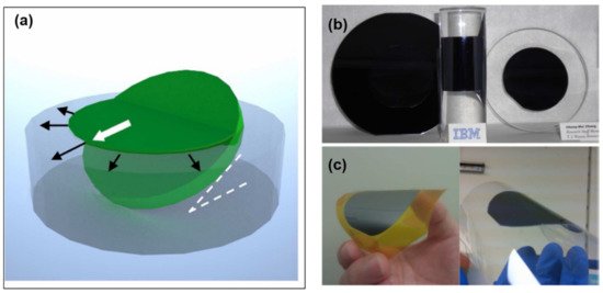
Figure 2. (a) Sketch of surface tension-assisted epitaxial lift-off (ELO) transfer techniques. (b) Demonstrations of the transferred GaAs thin films to the rigid substrate (left image, GaAs on 4′’ Si wafer. Center image, GaAs on curved solid object. Right image, GaAs on glass) and (c) flexible substrates (left, GaAs on tape. Right, GaAs on flexible sheet). Adapted from [3].
Releasing III-V semiconductor layers from the growth substrate to a receiving substrate by ELO has been researched for many years, and can be dated back to 1978. The ELO technique based on a lattice-matched release layer is now well developed, particularly for high-efficiency III-V solar cells [67][19][68][69].
2.2. ELO Assisted by Heterogeneous Release Layer
More recently, dissimilar release layers have also been explored, particularlyfor III-nitride layer release. Similar to III-V semiconductors, releasing III-nitride by ELO is also possible, but more challenging. Unlike III-V semiconductors, III-nitride layers themselves are resistant to most of etchant solvents and, therefore, they are not ideal release layers for GaN. To overcome this limit, most of efforts are therefore focused on introducing a dissimilar release layer rather than GaN alloy into the III-nitride epi-stack for ELO [17][20][30][32][41][42][44][45][50][60]. However, the epitaxial growth of GaN on a heterogeneous release layer is more challenging, and may lead to degraded material quality due to the lattice mismatch. Despite of these challenges, various release layers, including SiO2 [17][20][60], Ga2O3 [32], CrN [30], Nb2N [45], AlN [41][42], and ZnO [44][50], have been successfully explored to lift off GaN membranes.
Hsueh et al. demonstrated the use of ZnO as a sacrificial layer [50]. A 2-inch ZnO template layer was grown on a sapphire substrate by using pulsed laser deposition (PLD). The wafer was then loaded into an hydride organometallic vapor phase epitaxy (HOVPE) chamber for further growth of GaN epi-layers on top of the ZnO release layer. A low-pressure/temperature HOVPE approach was adopted to prevent ZnO decomposition. The completed wafer was then fixed onto a glass support using wax. Afterward, ELO was performed using HCL as an etchant solvent, resulting in the entire transfer of the 2-inch GaN epi-layer to the support substrate without apparent degradation of the GaN epi-layer. Due to the lateral etching mechanism, the etch rate at the wafer edge was found to be faster than in the wafer center. The surface of the released substrate was found to be very smooth, opening up the prospect of substrate reuse and cost reduction.
As another example of suitable release layers for GaN lift-off, CrN [30] was formed on a sapphire substrate by depositing chromium with a radio frequency (RF) sputtering system, followed by a nitridation process. LED layer structures were then grown on the CrN buffer/substrate by low-pressure HOVPE. A gold layer was electroplated to the p-GaN side to act as the support substrate. By selectively etching the CrN release layer using a mixture of H2O, Ce(NH4)2 (NO3)6, and HClO4, high-performance vertical LEDs transferred onto a gold support can be achieved. It was found that such vertical LEDs have much smaller serial resistance, showing the potential for general lighting. However, in this particular work, only centimeter-scale lift-off was realized. Whether it is suited for wafer-level ELO remains an open question.
Hsueh et al. demonstrated the use of Ga2O3 [32] as a release layer for III-nitride lift-off. LED layers grown on Ga2O3 can then be readily removed by HF, resulting in the transfer of 2-inch GaN LEDs to the electroplated Cu support. As GaN is inert to HF etching, the LED layer experiences minimal damage. One disadvantage of Ga2O3 is its decomposition under high temperatures in a H2-rich environment. Therefore, Ga2O3 must be grown separately in a N-rich atmosphere.
While various dissimilar release layer-assisted ELO techniques have been explored, great challenges remain for releasing III-nitride semiconductors. Thus far, the feasibility for commercial production of nitride compound semiconductors based on release layer-assisted ELO is not proven yet. The major challenges are relevant to the compromised epitaxy quality grown on a dissimilar sacrificial layer, and the etching-induced damage to the semiconductor layer to be released.
2.3. ELO Assisted by Micro/Nanopatterned Structures
In some cases, micro/nanopatterned structures can be used to assist the layer transfer [17]. In one example, nanoporous SiO2 [60] is formed by using an anodized alumina template as a mask. A GaN epi-layer is then grown on top of the nanoporous SiO2. After finishing the growth, wet etching of the nanoporous SiO2 using HF is performed, leading to the spontaneous release of the GaN film. The nanoporous SiO2 also facilitates the lateral epitaxial growth of high-quality GaN on the nanoporous SiO2, which can reduce the dislocation density in the epi-layer.
Void microstructures are also utilized to assist the layer release [18][42]. Lin et al. [42] demonstrated the growth of nitride semiconductors on a truncated triangle striped pattern sapphire substrate (Figure 3). This leads to the formation of an epi-stack with embedded void structures. These voids facilitate the wet etching of a thin AlN sacrificial layer in the lateral direction by hot KOH etching, leading to the formation of released GaN layers.
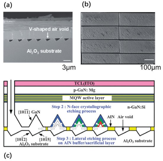
Figure 3. (a) An LED epitaxial layer was grown on the patterned sapphire substrate with V-shaped void channels. (b) The individual LED chips defined through the laser scribing process were lifted off from the void structures. (c) Schematic diagram of the multiple-quantum-well (MQW) LED structure topped with a transparent conductive layer (TCL) ITO for the chemical lift-off (CLO) process. Adapted with permission of [42]. Copyright Applied Physics Express, 2010.
2.4. Photoelectrochemical (PEC) or Electrochemical (EC) Etching
PEC etching methods [8][9][11][24][31][35][43][47][48][57][59][63] have been developed to release III-nitride, although conventional wet etching is difficult for etching III-nitride. This method exploits the illumination that only absorbs in the specific layer, in order to form electron–hole pairs in the semiconductor material [59]. The photogenerated holes result in the oxidation and dissolution of the semiconductor layer, while the electrons are moved to the cathode to participate in a reduction reaction. An example of PEC etching is demonstrated by Youtsey et al. [59]. The detailed PEC etching procedure is shown in Figure 4a. By selective PEC etching of an InGaN release layer, wafer-scale lift-off of 4-inch GaN films was demonstrated (Figure 4b).
Figure 4. (a) The detailed process flow of ELO based on photoelectrochemical (PEC) etching, and (b) full 4-inch GaN layer released by PEC etching. Adapted with permission from [59]. Copyright John Wiley and Sons, 2017.
In 2011, Lin et al. reported the lift-off of InGaN LED structures using a hybrid approach of PEC etching and mechanical peeling [43]. LED structures are prepatterned and fabricated on a sapphire substrate, followed by PEC lateral etching of the InGaN/GaN superlattices. A tape is then laminated onto the LED top. Mechanical peeling of the tape allows LEDs to be successfully transferred to the tape, with the emission blueshift to a shorter wavelength due to the strain relaxation. In a more recent work [11], similar PEC etching is conducted to release nanopillar LEDs defined by nanosphere lithography.
One of the disadvantages of PEC etching methods, however, is the requirement of external illumination sources. To address this issue, EC etching techniques without light illumination have also bene developed. For instance, Park et al. developed a method based on dope-selective EC etching to release GaN membranes [47]. The EC etching is fast for n-GaN but it is almost inert for p-GaN and undoped GaN. Making use of this highly selective etching, successful lift-off of patterned p-GaN films was achieved.
Modified EC etching methods for GaN release have also been developed [64]. Porous GaN formed by EC etching is exploited to assist the lift-off, whose porosity can be tuned by changing the doping concentration and adjusting the etching voltage. Zhang et al. [64] developed two different schemes for GaN layer transfer (Figure 5). In the first procedure (i.e, Procedure A shown in Figure 5a), two-stage EC etching was applied to n-doped GaN. Initially, a lower bias is applied to the GaN, and results in the formation of a porous GaN film of a certain depth. The bias is then increased in the second stage, leading to the formation of a void layer with larger porosity exactly below the porous layer generated in the first stage. Consequently, the GaN film can be released from the substrate. Alternatively, GaN release is also demonstrated based on a GaN sample with lightly doped n-GaN and heavily doped n-GaN, but only a constant bias is applied for conducting EC etching (Procedure B in Figure 5b). In this case, a void layer with larger porosity can be formed below lightly doped GaN. In both cases, centimeter-scale free-standing GaN membranes without degradation have been achieved. In the latter case, the thickness of the transferred layer can be accurately controlled by the doping concentration. However, wafer-scale release of GaN based on EC etching remains challenging.
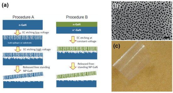
Figure 5. (a) Sketches of two different EC etching procedures, (b) SEM image of the porous structures formed by EC etching, and (c) the GaN membrane released from the porous GaN layer formed by EC etching. NP GaN in (a) stands for the nanoporous GaN. Adapted with permission from [64]. Copyright IOP Publishing, 2010.
In the above, successful lift-off of a single doped GaN layer from porous GaN formed by EC etching is demonstrated. This idea can be further extended to release InGaN/GaN MQW LED structures overgrown on a porous-GaN template formed by EC etching [62]. PEC- or EC-based transfer techniques have some advantages, compared with other ELO methods. Since the release layer is a GaN-based material (e.g., InGaN), the epi-layer quality can be maintained, and only one metal-organic chemical vapor deposition (MOCVD) growth cycle is needed, without introducing an extra dissimilar release layer which is commonly deposited by different equipment. One potential disadvantage, however, is the high surface roughness after lift-off. Furthermore, large-scale lift-off based on these techniques remains challenging.
3. Layer Transfer by Laser Lift-Off (LLO)
While ELO discussed in the previous section has achieved good success in some particular cases, the nature of wet etching also tends to cause partial damage to the semiconductor layer to be released. Finding a chemical etchant which is absolutely inert to the semiconductor layer but has a very high etch rate for the sacrificial layer is very difficult. The long etch duration for the wafer-level of ELO in many cases is also another constraint for fast production. Furthermore, wet etching is commonly not environmentally friendly, and is also hazardous in many cases. For these reasons, a few “dry” lift-off mechanisms are explored for layer transfer to minimize wet etching-induced damage and accelerate the lift-off.
One example of dry lift-off for layer release is LLO [70][71][72][73][74][75][76][77]. As schematically shown in Figure 1b, LLO makes use of the difference in absorption of the laser light between the substrate and the layer being released. In the case of GaN LEDs grown on a sapphire substrate, for example, the GaN epi-layer has a band gap of about 3.3 eV, whereas the sapphire band gap energy is ~ 9.9 eV. Short-wavelength laser light is therefore transparent for the sapphire, and but strongly absorbed in the GaN layer, thereby generating intense heat. This localized heat leads to the decomposition of the GaN near to the GaN/sapphire interface into Ga droplets and nitrogen gas, thereby separating the epi-layer from the substrate.
One particular application of this technique is the wafer-scale layer transfer of a GaN thin film to a support substrate. To assist the laser lift-off, the wafer is commonly fixed onto a temporary substrate by wafer bonding or adhesive bonding. One example [71] of such a strategy is demonstrated by Wang et al. (Figure 6). GaN wafer grown on sapphire was bonded with a Mo substrate using Ni/Au as the bonding layer. LLO was conducted to take off the sapphire substrate. A further bonding and subsequent annealing were applied to the released GaN layer on the Mo substrate. As a result, the resulting two-inch-diameter GaN template showed improved stability and a minimized stress state. Similarly, successful thin-layer transfer of 2-inch GaN via LLO has also been achieved by other support substrates including GaAs and polydimethylsiloxane (PDMS) [73].
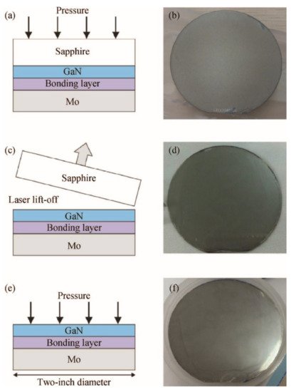
Figure 6. Schematic diagram of sample (a) after first bonding, (c) after laser-lift-off, and (e) after second bonding; image of the 2-inch-diameter sample after it went through (b) first bonding, (d) laser-lift-off, and (f) second bonding. Adapted with permission from [71]. Copyright IOP Science, 2016.
Many investigations indicate that LLO can also be used for fabricating free-standing GaN substrates with large thickness [70][73][75][76]. The free-standing GaN wafer size by LLO was limited to 1.5~2 inches in earlier investigations [75][76], but 4-inch free-standing GaN wafers have been demonstrated recently [70]. Major factors preventing the achievement of large, thick GaN templates include cracks induced by the thermal strain relaxation and laser-induced shock waves, causing damage at the N-polar face of GaN. It was reported that a heating plate above 800 degrees is helpful to release the compressive strain and avoid cracks during LLO. Laser spot size is another critical parameter affecting the laser-induced damage [70].
The laser lift-off technique is also applicable for fabricating flexible devices [78][72][74][79][80][81]. An example of the process flow for making flexible OLED displays based on LLO is shown in Figure 7. A sacrificial layer of polyimide [74] or α-GaOx [79] is formed on glass substrate. OLED devices are then formed on the sacrificial layer. Laser beam scanning results in intense heat generated in the interface between the sacrificial layer and glass substrate. Consequently, the sacrificial layer is ablated, resulting in the top OLEDs becoming delaminated from the substrate. This technique is now applied in large-volume production of flexible OLED display screens [74].
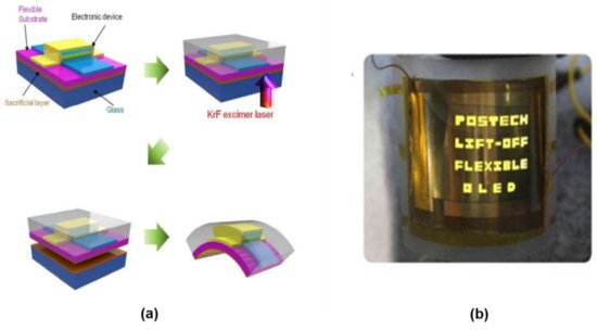
Figure 7. (a) Schematic diagram of the process flow for fabricating flexible OLED display by LLO. (b) The corresponding flexible OLED display fabricated by laser lift-off (LLO) based on the technology shown in (a). A 248 nm excimer KrF laser with a pulse width of 25 ns is used for the LLO. Adapted with permissions from [79]. Copyright Royal Society of Chemistry, 2014.
The LLO method is fast and scalable for any wafer size. For example, a 2” wafer, in principle, could be lifted off in a few seconds. However, in order to achieve high-quality transferred layers free from damage by laser lift-off, the beam quality and control must be well controlled. The cost of LLO facilities is another disadvantage that restricts its availability to regular users.
4. Layer Transfer by Mechanical Release
Mechanical release relies on mechanical force to separate the semiconductor layer from a growth substrate and transfer it to a support substrate. Broadly speaking, there are three major mechanical release approaches: spalling, 2D layer assisted peeling, and water-induced de-lamination.
4.1. Stress-Induced Delamination
Stress-induced delamination, or spalling [82][83][84][85][86][87][88][89][90][91][92], refers to a phenomenon where a layer with tensile stress tends to peel away from the substrate where the layer is grown, accompanied by the removal of a portion of the substrate material (Figure 8a). The mechanism behind spalling (or cracking) is due to the edge load created by the tensile stressor which guides the crack to be propagated at an equilibrium depth below the interface [83][85].
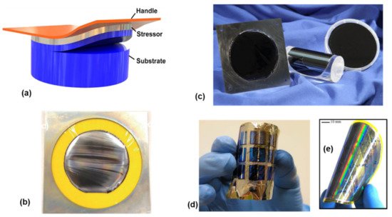
Figure 8. (a) Sketch of the mechanical spalling. Adapted from [86]. (b) Optical image of the released GaN film. Adapted with permission from [85]. Copyright IOP Science, 2013. (c) Optical images of Si on plastic mounted in a handling frame, 8 µm thick III–V multijunction layers on tape and mounted on a cylinder, and the bulk Si substrate from which the 20 µm thick layer was removed (from left to right). (d) Solar cells. Adapted with permission from [83]. Copyright IEEE, 2016. (e) flexible CMOS circuits fabricated by spalling techniques. Adapted with permission from [88]. Copyright American Chemical Society, 2012.
To achieve a controllable fracture and continuous film transfer, a tensile stressor layer with suitable thickness is coated on the substrate, followed by attaching a tape as the handle layer. A small force is then applied on the handle layer, resulting in forming a crack at a predetermined depth in the substrate. By mechanically guiding the handle layer, this crack can be guided and propagated in a controllable manner, resulting in transferring a portion of the material from the substrate to the handle layer [86].
This effect has been known for many years, and now it is possible to make use of this effect to achieve wafer-scale layer transfer of a variety of materials and devices, as shown in Figure 8. For example, silicon [82][87], InGaP/(In)GaAs [89], and GaN [85][91] have been successfully released by spalling. A wide range of flexible devices have also been demonstrated by spalling, including solar cells [83][84][89], LEDs [85][91], CMOS [86][88][92], etc. The figure below shows, for example, representative images of the full-wafer scale semiconductor layers and devices transferred by using this technique (Figure 8b–e).
Compared with epitaxial lift-off, stress-controlled spalling is much simpler, independent of area, and does not require the use of specialized etch layers. Substrate reuse is also demonstrated, opening up the prospect of cost reduction. One disadvantage of this technique, however, is fracture depth (or the thickness of the transferred layer) control, which is largely dependent on a variety of factors such as the stress amplitude, stress layer thickness, the stress layer material, and also the substrate material [86]. Accurate control of the thickness of the transferred layer induced by the spalling is therefore possible but extremely challenging. Another challenge lies in the residual stress and slight curvature that the layers possess after spalling. To process such thin, stressed films requires the development of particular film handling strategies and equipment. The third challenge lies in the high roughness of the released layer. For instance, roughnesses up to 500 nm root mean square (RMS) have been reported for released GaN [91]. The high roughness of the released layer is undesirable for subsequent device fabrication and integration.
4.2. 2D Layer-Assisted Delamination
2D layer-assisted delamination exploits the weak adhesion of the thin layer grown on layered 2D semiconductors [93][94][95][96][97][98][99][100][101][102][103][104][105][106][107][108][109][110]. This technique is also referred to as van der Waals (VDW) epitaxy [110] (Figure 9). Applying a mechanical force will break up the weak adhesion, and induce the delamination of the thin film from the 2D layered semiconductor. This method can potentially be used to obtain wafer-scale layer transfer at a low cost. Thanks to the advancement in epitaxial growth, VDW growth of high-quality III-nitride on such 2D semiconductor layers has been demonstrated, despite the large lattice mismatch. Various 2D layered materials, such as boron nitride [97][98][101][103] and graphene [93][94][95][96][99][100][102][104][105][106][107][108][109], have been explored to assist the lift-off of the thin semiconductor layers grown on 2D layered materials.
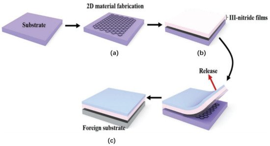
Figure 9. Schematic of 2D layer-assisted layer transfer, including three steps: (a) 2D material fabrication, (b) VDW epitaxy of III-nitride film, and (c) transfer printing onto foreign substrate. Adapted with permission from [110]. Copyright John Wiley and Sons, 2019.
Kobayashi et al. demonstrated the high quality of growth AlGaN/GaN LED layers on a boron nitride single-crystal layer [97]. The boron nitride layer has two functions. Besides the role for subsequent lift-off, it also acts as the buffer layer for nucleation of the high-quality AlGaN/GaN LED layer. To prevent from formation of polycrystalline GaN, an AlGaN layer is first deposited on the BN layer, followed by growing the final GaN LED layer structures. Due to its weak adhesion on the boron nitride, the LED layer can then be readily separated from the substrate to an indium sheet by weak peeling. Based on similar techniques, prototype vertical LEDs have also been demonstrated by the same group [98]. However, only centimeter-scale layer transfer has been demonstrated. Wafer-scale transfer based on BN needs to be explored. To overcome the size limit, one possible route is to grow a BN monolayer on a modified substrate with a quasi-3D mainspring shape in a furnace tube, instead of the conventional flat substrate [103]. This allows a high-quality h-BN monolayer with a size up to 25 inch to be grown, which can be then transferred to sapphire substrate for growing GaN. A 2-inch GaN wafer free of misfit strain grown on a BN monolayer has been achieved based on this technique.
Graphene-assisted growth has also been explored for fabricating free-standing semiconductor membranes [93][100][102][104]. Since the nucleation of atoms on a pristine graphene surface is remarkably suppressed due to the inert surface reactivity of graphene, earlier studies were therefore mainly focused on growing 3D microstructures on graphene. For instance, Chung et al. demonstrated the growth of regular GaN microdisk arrays on graphene dot patterns using epitaxial lateral overgrowth (ELOG) [102]. In another example, GaN microrods on graphene were demonstrated [100].
The 2D nucleation difficulty, however, can be overcome by introducing an intermediate layer. For instance, Chung et al. [94] demonstrated that ZnO nanowalls grown on graphene can assist the subsequent growth of 2D GaN LED layers (Figure 10). Due to the same crystal structure and small lattice mismatch with GaN, epitaxial GaN films are formed on the nanowalls in a manner similar to the lateral overgrowth, and eventually a flat GaN overgrowth layer can be formed. Such high-quality GaN LED layers grown on graphene allow the fabrication of LEDs transferred to various substrates, including glass, metal, and plastic, by simple mechanical peeling, and strong blue emissions have been obtained from such devices.
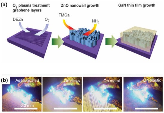
Figure 10. (a) Schematic illustrations of fabrication processes for epitaxial GaN thin films. (b) Optical images of light emissions from the as-fabricated LED on the original substrate and transferred LEDs on the foreign metal, glass, and plastic substrates. Adapted with permission from [94]. Copyright The American Association for the Advancement of Science, 2010.
In another study, to overcome the nucleation difficulty in 2D growth on graphene, an AlN buffer layer was introduced between the growth layer and graphene [105]. The graphene layer was grown on sapphire substrates by a catalyst-free atmospheric pressure chemical vapor deposition (APCVD) process, instead of using the complex transfer process of ex situ-grown graphene. An AlN buffer layer is then deposited on the nitrogen plasma-treated graphene to promote the GaN nucleation. The epitaxy is then finalized by growing GaN LED layers on the AlN/graphene buffer [105]. The APCVD method allows the high-quality growth of 2-inch single-crystal graphene. Due to the strain relaxation by the graphene, the as-prepared GaN shows significant improvements in the epitaxial quality, with a dislocation density as low as 1.7 × 107cm−2. The fabricated LED devices therefore are able to deliver much high optical power output than the device directly grown on sapphire.
Instead of using intermediate buffer layers, the nucleation difficulty can also be addressed by using a different growth strategy based on an off-angle substrate [93]. Such an off-angle substrate can remarkably promote the atom nucleation at the periodically distributed step edges, resulting in forming high-quality 2D materials grown directly on graphene. A good example based on this strategy is shown in the paper [93] (Figure 11). Miscut SiC substrates are used to grown graphene. Then, single-crystalline GaN films on graphene/SiC substrates are grown by using periodically distributed steps as the GaN nucleation sites. The following step is to deposit a stressor metal (Ni) and attach a thermal release tape to separate entire GaN films from the graphene surface and transfer the released GaN to host substrates. Fully functional blue light-emitting diodes (LEDs) have been demonstrated by this technique. SiC substrate reuse is also demonstrated.
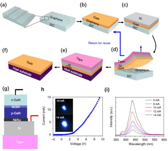
Figure 11. Schematic of a method for growing/transferring single-crystalline thin films on/from epitaxial graphene (a–f). (g) Schematic of a transferred visible LED device on the tape. (h) I–V characteristic of a transferred LED stack measured by applying positive bias on Ni and negative bias on n-GaN. The pictures of the LED emitting blue light are displayed in an inset. (i) Electroluminescence (EL) spectra of a transferred LED stack taken as a function of injection current. Adapted from [93].
Compared to the thermal, chemical, and mechanical approaches, the abovementioned strategy is a simple and feasible transfer technique with no need for additional procedures or equipment. This technique is similar to spalling, but one distinct merit is the accurate thickness control of the released layer—the thickness of the layer to be released is controlled by epitaxial growth, rather by the fracture depth decided by the stress amplitude. The other advantage is the reduced stress required for transfer, compared with spalling. Finally, the separation interface is smoother due to the 2D buffer layer not allowing covalent bonds between the epi-layer and the substrate.
4.3. Water-Assisted Delamination
Water-assisted delamination exploits the phenomenon of water-assisted debonding at the interface between a metallic layer (e.g., Ni) and an oxide layer (SiO2) [111][112][113]. This debonding in turn lifts off the upper layer from the original SiO2/Si substrate. The underlying mechanism is due to the water-induced decrease in the critical adhesion energy of the metal–SiO2 interface, which can be over 70% [112].
The discovery of this technique can be credited to Lee and coworkers [111][112]. An example [111] of an application using this technique is the transfer of thin-film solar cells (TFSCs) onto arbitrary substrates (Figure 12). TFSC films are deposited on Ni-coated SiO2/Si substrates, followed by standard microfabrication to form TFSC devices. A tape is attached to the TFSC surface as the temporary holder. The entire sample is then loaded into a water bath. A small peeling force is then applied at the tape edge to promote water penetration into the interface, and thus inducing the delamination of the TFSC devices from the substrate. The final step is transferring the released TFSC devices to the receiver substrates by sticking and removing the tape. Based on this technique, high-efficiency solar cells transferred to arbitrary substrates, such as cell phones, business cards, and glass windows, have been demonstrated. Such transferred devices maintained the same efficiency of 7.5%, implying no obvious degradation caused by the transfer process.
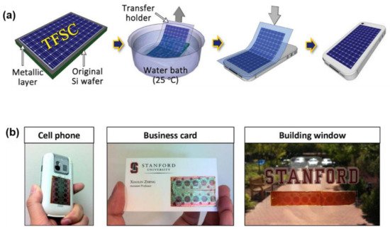
Figure 12. (a) Procedures of the peel-and-stick process. (b) Solar cells on cell phone (left), business card (middle), and building window (right). Adapted from [111].
In a more recent work [113], the same method is exploited to fabricate a wide range of thin-film nanoelectronic devices, such as a transferred Ag nanowirebased resistor, Si nanoribbon-based p-i-n diode, Si nanomembrane-based transistor, Si nanomembrane-based thin-film capacitors, nanomembrane-based MOSFETs, and a hybrid photodiode system that combines p-doped Si NM and n-doped MoS2 (Figure 13). The process has two primary steps: (i) transfer printing various single-crystalline semiconducting nanomaterials onto specific locations of a SiO2/Si wafer in a single device layout, followed by conventional CMOS fabrication to form electronic circuits on the wafer, and (ii) physically separating the entire layer of the completed thin-film nanoelectronics from the fabrication SiO2/Si wafer, which can be then pasted onto an arbitrary kind of supporting substrate or surface. The technique discussed here is wafer-recyclable, environmentally friendly, and cost-effective, showing good prospects for wafer-level production and integration of thin-film devices onto a single substrate.
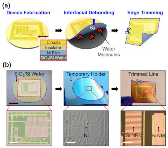
Figure 13. (a) Schematic illustrations of key steps for physically liberating thin-film nanoelectronics from a fabrication SiO2/Si wafer in water. (b) Optical images of the thin-film nanoelectronics on the SiO2/Si wafer (left), and peeled with a thermally releasable tape (middle), and then trimmed neatly (right). The bottom frame shows the corresponding microscope images. Si NRs in (b) stands for Si nanoribbons, and Si NM in (b) refers to Si nanomembrane. Adapted from [113].
5. Layer Transfer by Smart Cut
Smart Cut, or ion cut, is a technique of exploiting both ion implantation and wafer bonding to transfer ultrathin single-crystal layers from a donor substrate to a receiving substrate. This technology has been commercialized for the fabrication of silicon-on-insulator (SOI) wafers for many years [4], but it has also been explored for fabricating free-standing GaN membranes recently [114][115][116][117][118][119][120][121]. Taking splitting GaN, for example, the key processing steps of ion cut [114] are schematically shown in Figure 14a. A free-standing GaN template is prepared by depositing a thick GaN layer on a sapphire substrate, followed by LLO. The N-face of free-standing GaN is then implanted with H+ ions after lapping and chemical mechanical polishing. Argon atom beam irradiation on the N-face GaN and sapphire surfaces under vacuum is then conducted, in order to form chemically active dangling bonds. The next step is bonding the free-standing GaN to another sapphire substrate via plasma-treated hydrophilic bonding. Afterwards, the layer transfer is carried out in a furnace by annealing GaN/sapphire. Finally, the implantation-induced damaged layer on the low temperature grown GaN (LT-GaN) surface is removed using a dry etcher, resulting in LT-GaN transferred to the receiving wafer. Based on this technique, both a free-standing GaN template and GaN layer transferred to the receiving substrate with a wafer size up to 4 inches were demonstrated, as shown in Figure 14b,c.
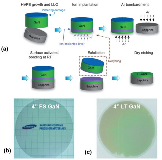
Figure 14. (a) Schematic illustrations of key steps for ion cutting techniques for GaN layer transfer. (b) Four-inch free-standing GaN template, and (c) transferred 4-inch GaN layer on the sapphire substrate. Adapted with permission from [114]. Copyright IOP Science, 2013.
One of the distinguishing features of the ion cut process is the production of multiple templates from a single donor wafer, thereby reducing the cost per template without compromising the crystalline quality. Another advantage is that the layer thickness can be finely controlled with nanometer-scale accuracy. For instance, with Smart Cut techniques, wafer-scale processed silicon films in the range of 0.2 to 1 µm in thickness have been reported.
References
- Lee, K.; Zimmerman, J.D.; Xiao, X.; Sun, K.; Forrest, S.R. Reuse of GaAs substrates for epitaxial lift-off by employing protection layers. J. Appl. Phys. 2012, 111, 033527.
- van Geelen, A.; Hageman, P.R.; Bauhuis, G.J.; van Rijsingen, P.C.; Schmidt, P.; Giling, L.J. Epitaxial lift-off GaAs solar cell from a reusable GaAs substrate. Mater. Sci. Eng. B 1997, 45, 162–171.
- Cheng, C.-W.; Shiu, K.-T.; Li, N.; Han, S.-J.; Shi, L.; Sadana, D.K. Epitaxial lift-off process for gallium arsenide substrate reuse and flexible electronics. Nat. Commun. 2013, 4, 1577.
- Bruel, M. Silicon on insulator material technology. Electron. Lett. 1995, 31, 1201.
- Wang, C.A.; Shiau, D.A.; Murphy, P.G.; O’Brien, P.W.; Huang, R.K.; Connors, M.K.; Anderson, A.C.; Donetsky, D.; Anikeev, S.; Belenky, G.; et al. Wafer bonding and epitaxial transfer of GaSb-based epitaxy to GaAs for monolithic interconnection of thermophotovoltaic devices. J. Electron. Mater. 2004, 33, 213–217.
- Kasai, S.; Tanabashi, A.; Kajiki, K.; Itsuji, T.; Kurosaka, R.; Yoneyama, H.; Yamashita, M.; Ito, H.; Ouchi, T. Micro Strip Line-Based On-Chip Terahertz Integrated Devices for High Sensitivity Biosensors. Appl. Phys. Express 2009, 2, 062401.
- Liang, D.; Fang, A.; Oakley, D.; Napoleone, A.; Chapman, D.; Chen, C.-L.; Juodawlkis, P.; Raday, O.; Bowers, J.E. 150 mm InP-to-Silicon Direct Wafer Bonding for Silicon Photonic Integrated Circuits. ECS Trans. 2019, 16, 235–241.
- Hwang, D.; Yonkee, B.P.; Addin, B.S.; Farrell, R.M.; Nakamura, S.; Speck, J.S.; DenBaars, S. Photoelectrochemical liftoff of LEDs grown on freestanding c-plane GaN substrates. Opt. Express 2016, 24, 22875–22880.
- Cao, D.; Xiao, H.; Gao, Q.; Yang, X.; Luan, C.; Mao, H.; Liu, J.; Liu, X. Fabrication and improved photoelectrochemical properties of a transferred GaN-based thin film with InGaN/GaN layers. Nanoscale 2017, 9, 11504–11510.
- Chan, L.; Karmstrand, T.; Chan, A.; Shapturenka, P.; Hwang, D.; Margalith, T.; DenBaars, S.P.; Gordon, M.J. Fabrication and chemical lift-off of sub-micron scale III-nitride LED structures. Opt. Express 2020, 28, 35038–35046.
- Chan, L.; Shapturenka, P.; Pynn, C.D.; Margalith, T.; DenBaars, S.P.; Gordon, M.J. Lift-off of semipolar blue and green III-nitride LEDs grown on free-standing GaN. Appl. Phys. Lett. 2020, 117, 021104.
- Chang, T.H.; Xiong, K.; Park, S.H.; Yuan, G.; Ma, Z.; Han, J. Strain Balanced AlGaN/GaN/AlGaN nanomembrane HEMTs. Sci. Rep. 2017, 7, 6360.
- Chen, D.; Han, J. High reflectance membrane-based distributed Bragg reflectors for GaN photonics. Appl. Phys. Lett. 2012, 101, 221104.
- Chen, D.; Xiao, H.; Han, J. Nanopores in GaN by electrochemical anodization in hydrofluoric acid: Formation and mechanism. J. Appl. Phys. 2012, 112, 064303.
- Chen, J.; Cheng, H.; Zhang, S.; Lan, F.; Qi, C.; Xu, Y.; Wang, Z.; Li, J.; Lai, Z. Fabrication of GaN Microporous Structure at a GaN/Sapphire Interface as the Template for Thick-Film GaN Separation Grown by HVPE. J. Electron. Mater. 2016, 45, 4782–4789.
- Cheng, C.-H.; Huang, T.-W.; Wu, C.-L.; Chen, M.K.; Chu, C.H.; Wu, Y.-R.; Shih, M.-H.; Lee, C.-K.; Kuo, H.-C.; Tsai, D.P.; et al. Transferring the bendable substrateless GaN LED grown on a thin C-rich SiC buffer layer to flexible dielectric and metallic plates. J. Mater. Chem. C 2017, 5, 607–617.
- Cho, C.-Y.; Lee, S.-J.; Hong, S.-H.; Park, S.-C.; Park, S.-E.; Park, Y.; Park, S.-J. Growth and Separation of High Quality GaN Epilayer from Sapphire Substrate by Lateral Epitaxial Overgrowth and Wet Chemical Etching. Appl. Phys. Express 2011, 4.
- Choi, J.H.; Cho, E.H.; Lee, Y.S.; Shim, M.-B.; Ahn, H.Y.; Baik, C.-W.; Lee, E.H.; Kim, K.; Kim, T.-H.; Kim, S.; et al. Fully Flexible GaN Light-Emitting Diodes through Nanovoid-Mediated Transfer. Adv. Opt. Mater. 2014, 2, 267–274.
- Choi, W.; Kim, C.Z.; Kim, C.S.; Heo, W.; Joo, T.; Ryu, S.Y.; Kim, H.; Kim, H.; Kang, H.K.; Jo, S. A Repeatable Epitaxial Lift-Off Process from a Single GaAs Substrate for Low-Cost and High-Efficiency III-V Solar Cells. Adv. Energy Mater. 2014, 4, 1400589.
- Chuang, S.-H.; Pan, C.-T.; Shen, K.-C.; Ou, S.-L.; Wuu, D.-S.; Horng, R.-H. Thin Film GaN LEDs Using a Patterned Oxide Sacrificial Layer by Chemical Lift-Off Process. IEEE Photonics Technol. Lett. 2013, 25, 2435–2438.
- Chung, J.W.; Piner, E.L.; Palacios, T. N-Face GaN/AlGaN HEMTs Fabricated Through Layer Transfer Technology. IEEE Electron Device Lett. 2009, 30, 113–116.
- Chyi, J.-I.; Fujioka, H.; Morkoç, H.; Nanishi, Y.; Schwarz, U.T.; Shim, J.-I.; Bayram, C. InGaN-based flexible light emitting diodes. In Proceedings of the Gallium Nitride Materials and Devices XII, San Francisco, CA, USA, 16 February 2017.
- Dong, J.; Wang, B.; Zou, X.; Zhao, W.; He, C.; He, L.; Wang, Q.; Chen, Z.; Li, S.; Zhang, K.; et al. Centimeter-long III-Nitride nanowires and continuous-wave pumped lasing enabled by graphically epitaxial lift-off. Nano Energy 2020, 78, 105404.
- ElAfandy, R.T.; Majid, M.A.; Ng, T.K.; Zhao, L.; Cha, D.; Ooi, B.S. Exfoliation of Threading Dislocation-Free, Single-Crystalline, Ultrathin Gallium Nitride Nanomembranes. Adv. Funct. Mater. 2014, 24, 2305–2311.
- Englhard, M.; Klemp, C.; Behringer, M.; Rudolph, A.; Skibitzki, O.; Zaumseil, P.; Schroeder, T. Characterization of reclaimed GaAs substrates and investigation of reuse for thin film InGaAlP LED epitaxial growth. J. Appl. Phys. 2016, 120, 045301.
- Englhard, M.; Reuters, B.; Michaelis, F.B.; Behringer, M.; Sundgren, P.; Klemp, C.; Skibitzki, O.; Schroeder, T. A novel vacuum epitaxial lift-off (VELO) process for separation of hard GaAs substrate/carrier systems for a more green semiconductor LED production. Mater. Sci. Semicond. Process. 2017, 71, 389–395.
- George, T.; Logeeswaran, V.J.; Islam, M.S.; Goodwin, J.; Katzenmeyer, A.M.; Dutta, A.K.; Islam, M.S. Heterogeneous 3D integration of multi-spectral photonic sensor with highly oriented micro/nano-pillars of semiconductors. In Proceedings of the Micro and Nanotechnology Sensors, Systems, and Applications, Orlando, FL, USA, 11 May 2009.
- Geum, D.M.; Kim, S.; Kim, S.K.; Kang, S.; Kyhm, J.; Song, J.; Choi, W.J.; Yoon, E. Monolithic integration of visible GaAs and near-infrared InGaAs for multicolor photodetectors by using high-throughput epitaxial lift-off toward high-resolution imaging systems. Sci. Rep. 2019, 9, 18661.
- Glavin, N.R.; Chabak, K.D.; Heller, E.R.; Moore, E.A.; Prusnick, T.A.; Maruyama, B.; Walker, D.E., Jr.; Dorsey, D.L.; Paduano, Q.; Snure, M. Flexible Gallium Nitride for High-Performance, Strainable Radio-Frequency Devices. Adv. Mater. 2017, 29, 1701838.
- Ha, J.-S.; Lee, S.W.; Lee, H.-J.; Lee, H.-J.; Lee, S.H.; Goto, H.; Kato, T.; Fujii, K.; Cho, M.W.; Yao, T. The Fabrication of Vertical Light-Emitting Diodes Using Chemical Lift-Off Process. IEEE Photonics Technol. Lett. 2008, 20, 175–177.
- Hsieh, C.; Chen, H.-S.; Liao, C.-H.; Chen, C.-Y.; Lin, C.-H.; Lin, C.-H.; Ting, S.-Y.; Yao, Y.-F.; Chen, H.-T.; Kiang, Y.-W.; et al. Photoelectrochemical Liftoff of Patterned Sapphire Substrate for Fabricating Vertical Light-Emitting Diode. IEEE Photonics Technol. Lett. 2012, 24, 1775–1777.
- Hsueh, H.-H.; Ou, S.-L.; Wuu, D.-S.; Horng, R.-H. InGaN LED fabricated on Eco-GaN template with a Ga2O3 sacrificial layer for chemical lift-off application. Vacuum 2015, 118, 8–12.
- Huang, S.; Zhang, Y.; Leung, B.; Yuan, G.; Wang, G.; Jiang, H.; Fan, Y.; Sun, Q.; Wang, J.; Xu, K.; et al. Mechanical properties of nanoporous GaN and its application for separation and transfer of GaN thin films. ACS Appl Mater Interfaces 2013, 5, 11074–11079.
- Huo, Q.; Shao, Y.; Wu, Y.; Zhang, B.; Hu, H.; Hao, X. High quality self-separated GaN crystal grown on a novel nanoporous template by HVPE. Sci. Rep. 2018, 8, 3166.
- Jiang, J.; Dong, J.; Wang, B.; He, C.; Zhao, W.; Chen, Z.; Zhang, K.; Wang, X. Epitaxtial lift-off for freestanding InGaN/GaN membranes and vertical blue light-emitting-diodes. J. Mater. Chem. C 2020, 8, 8284–8289.
- Kang, K.; Lee, K.H.; Han, Y.; Gao, H.; Xie, S.; Muller, D.A.; Park, J. Layer-by-layer assembly of two-dimensional materials into wafer-scale heterostructures. Nature 2017, 550, 229–233.
- Lee, D.; Cherekdjian, S.; Kang, S.; Mishra, K.; Ong, P.; Xu, X. 18-2: Ultra-Fine High Efficiency MicroLEDs with Testability and Transferability Using Layer-Transfer Technology. SID Symp. Dig. Tech. Pap. 2019, 50, 236–239.
- Lee, S.; Kim, S.K.; Han, J.-H.; Song, J.D.; Jun, D.-H.; Kim, S.-H. Epitaxial Lift-Off Technology for Large Size III–V-on-Insulator Substrate. IEEE Electron Device Lett. 2019, 40, 1732–1735.
- Lesecq, M.; Hoel, V.; Lecavelier des Etangs-Levallois, A.; Pichonat, E.; Douvry, Y.; De Jaeger, J.C. High Performance of AlGaN/GaN HEMTs Reported on Adhesive Flexible Tape. IEEE Electron Device Lett. 2011, 32, 143–145.
- Li, Y.; Zhao, Y.; Wei, T.; Liu, Z.; Duan, R.; Wang, Y.; Zhang, X.; Wu, Q.; Yan, J.; Yi, X.; et al. Van der Waals epitaxy of GaN-based light-emitting diodes on wet-transferred multilayer graphene film. Jpn. J. Appl. Phys. 2017, 56, 85506.
- Lin, C.-F.; Dai, J.-J.; Lin, M.-S.; Chen, K.-T.; Huang, W.-C.; Lin, C.-M.; Jiang, R.-H.; Huang, Y.-C. An AlN Sacrificial Buffer Layer Inserted into the GaN/Patterned Sapphire Substrate for a Chemical Lift-Off Process. Appl. Phys. Express 2010, 3, 31001.
- Lin, C.-F.; Dai, J.-J.; Wang, G.-M.; Lin, M.-S. Chemical Lift-Off Process for Blue Light-Emitting Diodes. Appl. Phys. Express 2010, 3, 092101.
- Lin, M.-S.; Lin, C.-F.; Huang, W.-C.; Wang, G.-M.; Shieh, B.-C.; Dai, J.-J.; Chang, S.-Y.; Wuu, D.S.; Liu, P.-L.; Horng, R.-H. Chemical–Mechanical Lift-Off Process for InGaN Epitaxial Layers. Appl. Phys. Express 2011, 4, 062101.
- Liu, H.F.; Liu, W.; Chua, S.J. Epitaxial growth and chemical lift-off of GaInN/GaN heterostructures on c- and r-sapphire substrates employing ZnO sacrificial templates. J. Vac. Sci. Technol. A Vac. Surf. Films 2010, 28, 590–594.
- Meyer, D.J.; Downey, B.P.; Katzer, D.S.; Nepal, N.; Wheeler, V.D.; Hardy, M.T.; Anderson, T.J.; Storm, D.F. Epitaxial Lift-Off and Transfer of III-N Materials and Devices from SiC Substrates. IEEE Trans. Semicond. Manuf. 2016, 29, 384–389.
- O’Callaghan, J.; Loi, R.; Mura, E.E.; Roycroft, B.; Trindade, A.J.; Thomas, K.; Gocalinska, A.; Pelucchi, E.; Zhang, J.; Roelkens, G.; et al. Comparison of InGaAs and InAlAs sacrificial layers for release of InP-based devices. Opt. Mater. Express 2017, 7, 4408.
- Park, J.; Song, K.M.; Jeon, S.-R.; Baek, J.H.; Ryu, S.-W. Doping selective lateral electrochemical etching of GaN for chemical lift-off. Appl. Phys. Lett. 2009, 94, 221907.
- Park, S.H.; Yuan, G.; Chen, D.; Xiong, K.; Song, J.; Leung, B.; Han, J. Wide bandgap III-nitride nanomembranes for optoelectronic applications. Nano Lett. 2014, 14, 4293–4298.
- Pasayat, S.S.; Gupta, C.; Wong, M.S.; Wang, Y.; Nakamura, S.; Denbaars, S.P.; Keller, S.; Mishra, U.K. Growth of strain-relaxed InGaN on micrometer-sized patterned compliant GaN pseudo-substrates. Appl. Phys. Lett. 2020, 116, 111101.
- Rajan, A.; Rogers, D.J.; Ton-That, C.; Zhu, L.; Phillips, M.R.; Sundaram, S.; Gautier, S.; Moudakir, T.; El-Gmili, Y.; Ougazzaden, A.; et al. Wafer-scale epitaxial lift-off of optoelectronic grade GaN from a GaN substrate using a sacrificial ZnO interlayer. J. Phys. D Appl. Phys. 2016, 49, 315105.
- Schermer, J.J.; Bauhuis, G.J.; Mulder, P.; Meulemeesters, W.J.; Haverkamp, E.; Voncken, M.M.A.J.; Larsen, P.K. High rate epitaxial lift-off of InGaP films from GaAs substrates. Appl. Phys. Lett. 2000, 76, 2131–2133.
- Schermer, J.J.; Mulder, P.; Bauhuis, G.J.; Voncken, M.M.A.J.; van Deelen, J.; Haverkamp, E.; Larsen, P.K. Epitaxial Lift-Off for large area thin film III/V devices. Phys. Status Solidi 2005, 202, 501–508.
- Voncken, M.M.A.J.; Schermer, J.J.; Bauhuis, G.J.; Mulder, P.; Larsen, P.K. Multiple release layer study of the intrinsic lateral etch rate of the epitaxial lift-off process. Appl. Phys. A 2004, 79, 1801–1807.
- Vuong, P.; Sundaram, S.; Mballo, A.; Patriarche, G.; Leone, S.; Benkhelifa, F.; Karrakchou, S.; Moudakir, T.; Gautier, S.; Voss, P.L.; et al. Control of the Mechanical Adhesion of III-V Materials Grown on Layered h-BN. ACS Appl. Mater. Interfaces 2020, 12, 55460–55466.
- Wu, F.L.; Ou, S.L.; Kao, Y.C.; Chen, C.L.; Tseng, M.C.; Lu, F.C.; Lin, M.T.; Horng, R.H. Thin-film vertical-type AlGaInP LEDs fabricated by epitaxial lift-off process via the patterned design of Cu substrate. Opt. Express 2015, 23, 18156–18165.
- Xiong, K.; Mi, H.; Chang, T.-H.; Liu, D.; Xia, Z.; Wu, M.-Y.; Yin, X.; Gong, S.; Zhou, W.; Shin, J.C.; et al. AlGaAs/Si dual-junction tandem solar cells by epitaxial lift-off and print-transfer-assisted direct bonding. Energy Sci. Eng. 2018, 6, 47–55.
- Xiong, K.; Park, S.H.; Song, J.; Yuan, G.; Chen, D.; Leung, B.; Han, J. Single Crystal Gallium Nitride Nanomembrane Photoconductor and Field Effect Transistor. Adv. Funct. Mater. 2014, 24, 6503–6508.
- Yang, W.; Yang, H.; Qin, G.; Ma, Z.; Berggren, J.; Hammar, M.; Soref, R.; Zhou, W. Large-area InP-based crystalline nanomembrane flexible photodetectors. Appl. Phys. Lett. 2010, 96, 121107.
- Youtsey, C.; McCarthy, R.; Reddy, R.; Forghani, K.; Xie, A.; Beam, E.; Wang, J.; Fay, P.; Ciarkowski, T.; Carlson, E.; et al. Wafer-scale epitaxial lift-off of GaN using bandgap-selective photoenhanced wet etching. Phys. Status Solidi 2017, 254, 1600774.
- Zang, K.; Cheong, D.; Liu, H.; Liu, H.; Teng, J.; Chua, S. A New Method for Lift-off of III-Nitride Semiconductors for Heterogeneous Integration. Nanoscale Res. Lett. 2010, 5, 1051–1056.
- Zhang, B.; Egawa, T.; Ishikawa, H.; Liu, Y.; Jimbo, T. Thin-film InGaN multiple-quantum-well light-emitting diodes transferred from Si (111) substrate onto copper carrier by selective lift-off. Appl. Phys. Lett. 2005, 86, 071113.
- Zhang, Y.; Leung, B.; Han, J. A liftoff process of GaN layers and devices through nanoporous transformation. Appl. Phys. Lett. 2012, 100, 181908.
- Zhang, Y.; Ryu, S.-W.; Yerino, C.; Leung, B.; Sun, Q.; Song, Q.; Cao, H.; Han, J. A conductivity-based selective etching for next generation GaN devices. Phys. Status Solidi 2010, 247, 1713–1716.
- Zhang, Y.; Sun, Q.; Leung, B.; Simon, J.; Lee, M.L.; Han, J. The fabrication of large-area, free-standing GaN by a novel nanoetching process. NanoTechnology 2011, 22, 045603.
- Zhao, C.; Ng, T.K.; Tseng, C.-C.; Li, J.; Shi, Y.; Wei, N.; Zhang, D.; Consiglio, G.B.; Prabaswara, A.; Alhamoud, A.A.; et al. InGaN/GaN nanowires epitaxy on large-area MoS2 for high-performance light-emitters. RSC Adv. 2017, 7, 26665–26672.
- Chang, T.-H.; Fan, W.; Liu, D.; Xia, Z.; Ma, Z.; Liu, S.; Menon, L.; Yang, H.; Zhou, W.; Berggren, J.; et al. Selective release of InP heterostructures from InP substrates. J. Vac. Sci. Technol. B Nanotechnol. Microelectron. Mater. Process. Meas. Phenom. 2016, 34, 041229.
- Bauhuis, G.J.; Mulder, P.; Haverkamp, E.J.; Huijben, J.C.C.M.; Schermer, J.J. 26.1% thin-film GaAs solar cell using epitaxial lift-off. Solar Energy Mater. Solar Cells 2009, 93, 1488–1491.
- Kirk, A.P.; Cardwell, D.W.; Wood, J.D.; Wibowo, A.; Forghani, K.; Rowell, D.; Pan, N.; Osowski, M. Recent Progress in Epitaxial Lift-Off Solar Cells. Proceedings of 2018 IEEE 7th World Conference on Photovoltaic Energy Conversion (WCPEC) (A Joint Conference of 45th IEEE PVSC, 28th PVSEC & 34th EU PVSEC), Waikoloa HI, USA, 10–15 June 2018; pp. 32–35.
- Moon, S.; Kim, K.; Kim, Y.; Heo, J.; Lee, J. Highly efficient single-junction GaAs thin-film solar cell on flexible substrate. Sci. Rep. 2016, 6, 30107.
- Xu, K.; Wang, J.-F.; Ren, G.-Q. Progress in bulk GaN growth. Chin. Phys. B 2015, 24, 066105.
- Wang, Q.; Liu, Y.; Sun, Y.; Tong, Y.; Zhang, G. Fabrication of extremely thermal-stable GaN template on Mo substrate using double bonding and step annealing process. J. Semicond. 2016, 37, 083001.
- Seo, J.-H.; Li, J.; Lee, J.; Gong, S.; Lin, J.; Jiang, H.; Ma, Z. A Simplified Method of Making Flexible Blue LEDs on a Plastic Substrate. IEEE Photonics J. 2015, 7, 1–7.
- Miskys, C.R.; Kelly, M.K.; Ambacher, O.; Stutzmann, M. Freestanding GaN-substrates and devices. Phys. Status Solidi 2003, 1627–1650.
- Delmdahl, R.; Pätzel, R.; Brune, J. Large-Area Laser-Lift-Off Processing in Microelectronics. Phys. Procedia 2013, 41, 241–248.
- Kelly, M.K.; Vaudo, R.P.; Phanse, V.M.; Görgens, L.; Ambacher, O.; Stutzmann, M. Large Free-Standing GaN Substrates by Hydride Vapor Phase Epitaxy and Laser-Induced Liftoff. Jpn. J. Appl. Phys. 1999, 38, L217–L219.
- Park, S.S.; Park, I.-W.; Choh, S.H. Free-Standing GaN Substrates by Hydride Vapor Phase Epitaxy. Jpn. J. Appl. Phys. 2000, 39, L1141–L1142.
- Ueda, T.; Ishida, M.; Yuri, M. Separation of Thin GaN from Sapphire by Laser Lift-Off Technique. Jpn. J. Appl. Phys. 2011, 50, 041001.
- Mohseni, H.; Lee, S.H.; Park, S.Y.; Lee, K.J.; Agahi, M.H.; Razeghi, M. Laser lift-off of GaN thin film and its application to the flexible light emitting diodes. Proceedings of Biosensing and Nanomedicine V, Sand Diego, CA, USA, 10 October 2012; p. 846011.
- Kim, K.; Kim, S.Y.; Lee, J.-L. Flexible organic light-emitting diodes using a laser lift-off method. J. Mater. Chem. C 2014, 2, 2144.
- Tian, Z.; Li, Y.; Su, X.; Feng, L.; Wang, S.; Ding, W.; Li, Q.; Zhang, Y.; Guo, M.; Yun, F.; et al. Super flexible GaN light emitting diodes using microscale pyramid arrays through laser lift-off and dual transfer. Opt. Express 2018, 26, 1817–1824.
- Kim, S.J.; Lee, H.E.; Choi, H.; Kim, Y.; We, J.H.; Shin, J.S.; Lee, K.J.; Cho, B.J. High-Performance Flexible Thermoelectric Power Generator Using Laser Multiscanning Lift-Off Process. ACS Nano 2016, 10, 10851–10857.
- Dross, F.; Robbelein, J.; Vandevelde, B.; Van Kerschaver, E.; Gordon, I.; Beaucarne, G.; Poortmans, J. Stress-induced large-area lift-off of crystalline Si films. Appl. Phys. A 2007, 89, 149–152.
- Bedell, S.W.; Shahrjerdi, D.; Hekmatshoar, B.; Fogel, K.; Lauro, P.A.; Ott, J.A.; Sosa, N.; Sadana, D. Kerf-Less Removal of Si, Ge, and III–V Layers by Controlled Spalling to Enable Low-Cost PV Technologies. IEEE J. Photovolt. 2012, 2, 141–147.
- Shahrjerdi, D.; Bedell, S.W.; Ebert, C.; Bayram, C.; Hekmatshoar, B.; Fogel, K.; Lauro, P.; Gaynes, M.; Gokmen, T.; Ott, J.A.; et al. High-efficiency thin-film InGaP/InGaAs/Ge tandem solar cells enabled by controlled spalling technology. Appl. Phys. Lett. 2012, 100, 053901.
- Bedell, S.W.; Bayram, C.; Fogel, K.; Lauro, P.; Kiser, J.; Ott, J.; Zhu, Y.; Sadana, D. Vertical Light-Emitting Diode Fabrication by Controlled Spalling. Appl. Phys. Express 2013, 6, 112301.
- Bedell, S.W.; Fogel, K.; Lauro, P.; Shahrjerdi, D.; Ott, J.A.; Sadana, D. Layer transfer by controlled spalling. J. Phys. D Appl. Phys. 2013, 46, 152002.
- Kwon, Y.; Yang, C.; Yoon, S.-H.; Um, H.-D.; Lee, J.-H.; Yoo, B. Spalling of a Thin Si Layer by Electrodeposit-Assisted Stripping. Appl. Phys. Express 2013, 6, 116502.
- Shahrjerdi, D.; Bedell, S.W. Extremely flexible nanoscale ultrathin body silicon integrated circuits on plastic. Nano Lett. 2013, 13, 315–320.
- Shahrjerdi, D.; Bedell, S.W.; Bayram, C.; Lubguban, C.C.; Fogel, K.; Lauro, P.; Ott, J.A.; Hopstaken, M.; Gayness, M.; Sadana, D. Ultralight High-Efficiency Flexible InGaP/(In)GaAs Tandem Solar Cells on Plastic. Adv. Energy Mater. 2013, 3, 566–571.
- Sweet, C.A.; Schulte, K.L.; Simon, J.D.; Steiner, M.A.; Jain, N.; Young, D.L.; Ptak, A.J.; Packard, C.E. Controlled exfoliation of (100) GaAs-based devices by spalling fracture. Appl. Phys. Lett. 2016, 108, 011906.
- Bedell, S.W.; Lauro, P.; Ott, J.A.; Fogel, K.; Sadana, D.K. Layer transfer of bulk gallium nitride by controlled spalling. J. Appl. Phys. 2017, 122, 025103.
- Park, H.; Lim, C.; Noh, Y.; Lee, C.-J.; Won, H.; Jung, J.; Choi, M.; Kim, J.-J.; Yoo, H.; Park, H. Investigation of electrical characteristics of flexible CMOS devices fabricated with thickness-controlled spalling process. Solid-State Electron. 2020, 173, 107901.
- Kim, J.; Bayram, C.; Park, H.; Cheng, C.W.; Dimitrakopoulos, C.; Ott, J.A.; Reuter, K.B.; Bedell, S.W.; Sadana, D.K. Principle of direct van der Waals epitaxy of single-crystalline films on epitaxial graphene. Nat. Commun. 2014, 5, 4836.
- Chung, K.; Lee, C.H.; Yi, G.C. Transferable GaN layers grown on ZnO-coated graphene layers for optoelectronic devices. Science 2010, 330, 655–657.
- Lin, Y.M.; Dimitrakopoulos, C.; Jenkins, K.A.; Farmer, D.B.; Chiu, H.Y.; Grill, A.; Avouris, P. 100-GHz transistors from wafer-scale epitaxial graphene. Science 2010, 327, 662.
- Chung, K.; In Park, S.; Baek, H.; Chung, J.-S.; Yi, G.-C. High-quality GaN films grown on chemical vapor-deposited graphene films. NPG Asia Mater. 2012, 4, e24.
- Kobayashi, Y.; Kumakura, K.; Akasaka, T.; Makimoto, T. Layered boron nitride as a release layer for mechanical transfer of GaN-based devices. Nature 2012, 484, 223–227.
- Makimoto, T.; Kumakura, K.; Kobayashi, Y.; Akasaka, T.; Yamamoto, H. A Vertical InGaN/GaN Light-Emitting Diode Fabricated on a Flexible Substrate by a Mechanical Transfer Method Using BN. Appl. Phys. Express 2012, 5, 072102.
- Nepal, N.; Wheeler, V.D.; Anderson, T.J.; Kub, F.J.; Mastro, M.A.; Myers-Ward, R.L.; Qadri, S.B.; Freitas, J.A.; Hernandez, S.C.; Nyakiti, L.O.; et al. Epitaxial Growth of III–Nitride/Graphene Heterostructures for Electronic Devices. Appl. Phys. Express 2013, 6, 061003.
- Chung, K.; Beak, H.; Tchoe, Y.; Oh, H.; Yoo, H.; Kim, M.; Yi, G.-C. Growth and characterizations of GaN micro-rods on graphene films for flexible light emitting diodes. APL Mater. 2014, 2, 092512.
- Ayari, T.; Sundaram, S.; Li, X.; El Gmili, Y.; Voss, P.L.; Salvestrini, J.P.; Ougazzaden, A. Wafer-scale controlled exfoliation of metal organic vapor phase epitaxy grown InGaN/GaN multi quantum well structures using low-tack two-dimensional layered h-BN. Appl. Phys. Lett. 2016, 108, 171106.
- Chung, K.; Yoo, H.; Hyun, J.K.; Oh, H.; Tchoe, Y.; Lee, K.; Baek, H.; Kim, M.; Yi, G.C. Flexible GaN Light-Emitting Diodes Using GaN Microdisks Epitaxial Laterally Overgrown on Graphene Dots. Adv. Mater. 2016, 28, 7688–7694.
- Wu, C.; Soomro, A.M.; Sun, F.; Wang, H.; Huang, Y.; Wu, J.; Liu, C.; Yang, X.; Gao, N.; Chen, X.; et al. Large-roll growth of 25-inch hexagonal BN monolayer film for self-release buffer layer of free-standing GaN wafer. Sci. Rep. 2016, 6, 34766.
- Kim, Y.; Cruz, S.S.; Lee, K.; Alawode, B.O.; Choi, C.; Song, Y.; Johnson, J.M.; Heidelberger, C.; Kong, W.; Choi, S.; et al. Remote epitaxy through graphene enables two-dimensional material-based layer transfer. Nature 2017, 544, 340–343.
- Chen, Z.; Zhang, X.; Dou, Z.; Wei, T.; Liu, Z.; Qi, Y.; Ci, H.; Wang, Y.; Li, Y.; Chang, H.; et al. High-Brightness Blue Light-Emitting Diodes Enabled by a Directly Grown Graphene Buffer Layer. Adv. Mater. 2018, 30, e1801608.
- Chang, H.; Chen, Z.; Li, W.; Yan, J.; Hou, R.; Yang, S.; Liu, Z.; Yuan, G.; Wang, J.; Li, J.; et al. Graphene-assisted quasi-van der Waals epitaxy of AlN film for ultraviolet light emitting diodes on nano-patterned sapphire substrate. Appl. Phys. Lett. 2019, 114, 091107.
- Ci, H.; Chang, H.; Wang, R.; Wei, T.; Wang, Y.; Chen, Z.; Sun, Y.; Dou, Z.; Liu, Z.; Li, J.; et al. Enhancement of Heat Dissipation in Ultraviolet Light-Emitting Diodes by a Vertically Oriented Graphene Nanowall Buffer Layer. Adv. Mater. 2019, 31, e1901624.
- Jia, Y.; Ning, J.; Zhang, J.; Yan, C.; Wang, B.; Zhang, Y.; Zhu, J.; Shen, X.; Dong, J.; Wang, D.; et al. Transferable GaN Enabled by Selective Nucleation of AlN on Graphene for High-Brightness Violet Light-Emitting Diodes. Adv. Opt. Mater. 2019, 8, 1901632.
- Liu, F.; Zhang, Z.; Rong, X.; Yu, Y.; Wang, T.; Sheng, B.; Wei, J.; Zhou, S.; Yang, X.; Xu, F.; et al. Graphene-Assisted Epitaxy of Nitrogen Lattice Polarity GaN Films on Non-Polar Sapphire Substrates for Green Light Emitting Diodes. Adv. Funct. Mater. 2020, 30, 2001283.
- Yu, J.; Wang, L.; Hao, Z.; Luo, Y.; Sun, C.; Wang, J.; Han, Y.; Xiong, B.; Li, H. Van der Waals Epitaxy of III-Nitride Semiconductors Based on 2D Materials for Flexible Applications. Adv. Mater. 2020, 32, e1903407.
- Lee, C.H.; Kim, D.R.; Cho, I.S.; William, N.; Wang, Q.; Zheng, X. Peel-and-stick: Fabricating thin film solar cell on universal substrates. Sci. Rep. 2012, 2, 1000.
- Lee, C.H.; Kim, J.H.; Zou, C.; Cho, I.S.; Weisse, J.M.; Nemeth, W.; Wang, Q.; van Duin, A.C.; Kim, T.S.; Zheng, X. Peel-and-stick: Mechanism study for efficient fabrication of flexible/transparent thin-film electronics. Sci. Rep. 2013, 3, 2917.
- Wie, D.S.; Zhang, Y.; Kim, M.K.; Kim, B.; Park, S.; Kim, Y.J.; Irazoqui, P.P.; Zheng, X.; Xu, B.; Lee, C.H. Wafer-recyclable, environment-friendly transfer printing for large-scale thin-film nanoelectronics. Proc. Natl. Acad. Sci. USA 2018, 115, E7236–E7244.
- Chung, R.B.-K.; Kim, D.; Lim, S.-K.; Choi, J.-S.; Kim, K.-J.; Lee, B.-H.; Jung, K.S.; Kim-Lee, H.-J.; Lee, W.J.; Park, B.; et al. Layer-Transferred GaN Template by Ion Cut for Nitride-Based Light-Emitting Diodes. Appl. Phys. Express 2013, 6, 111005.
- Tapily, K.; Moutanabbir, O.; Abdullah, M.; Gu, D.; Baumgart, H.; Elmustafa, A. Hydrogen Ion-Induced AlN Thin Layer Transfer: An Elastomechanical Study. ECS Trans. 2019, 33, 255–261.
- Tauzin, A.; Akatsu, T.; Rabarot, M.; Dechamp, J.; Zussy, M.; Moriceau, H.; Michaud, J.F.; Charvet, A.M.; Di Cioccio, L.; Fournel, F.; et al. Transfers of 2-inch GaN films onto sapphire substrates using Smart CutTM technology. Electron. Lett. 2005, 41, 668.
- Dadwal, U.; Scholz, R.; Reiche, M.; Kumar, P.; Chandra, S.; Singh, R. Effect of implantation temperature on the blistering behavior of hydrogen implanted GaN. Appl. Phys. A 2012, 112, 451–456.
- Iwinska, M.; Amilusik, M.; Fijalkowski, M.; Sochacki, T.; Lucznik, B.; Grzanka, E.; Litwin-Staszewska, E.; Weyher, J.L.; Nowakowska-Siwinska, A.; Muziol, G.; et al. HVPE-GaN growth on GaN-based Advanced Substrates by Smart Cut™. J. Cryst. Growth 2016, 456, 73–79.
- Huang, K.; Jia, Q.; You, T.; Zhang, R.; Lin, J.; Zhang, S.; Zhou, M.; Zhang, B.; Yu, W.; Ou, X.; et al. Investigation on thermodynamics of ion-slicing of GaN and heterogeneously integrating high-quality GaN films on CMOS compatible Si(100) substrates. Sci. Rep. 2017, 7, 15017.
- Min Lee, S.; Hwan Yum, J.; Larsen, E.S.; Chul Lee, W.; Keun Kim, S.; Bielawski, C.W.; Oh, J. Advanced Silicon-on-Insulator: Crystalline Silicon on Atomic Layer Deposited Beryllium Oxide. Sci. Rep. 2017, 7, 13205.
- Nguyen, B.-Y.; Mazuré, C.; Celler, G. Substrate Engineering for 32nm and Beyond. ECS Trans. 2019, 22, 91–98.

