Your browser does not fully support modern features. Please upgrade for a smoother experience.
Submitted Successfully!
 +1 credit
Thank you for your contribution! You can also upload a video entry or images related to this topic.
For video creation, please contact our Academic Video Service.
| Version | Summary | Created by | Modification | Content Size | Created at | Operation |
|---|---|---|---|---|---|---|
| 1 | Satyendra Kumar Mishra | -- | 5511 | 2024-03-28 10:07:11 | | | |
| 2 | Camila Xu | Meta information modification | 5511 | 2024-04-01 07:47:23 | | | | |
| 3 | Dean Liu | Meta information modification | 5511 | 2024-06-11 05:04:41 | | |
Video Upload Options
We provide professional Academic Video Service to translate complex research into visually appealing presentations. Would you like to try it?
Cite
If you have any further questions, please contact Encyclopedia Editorial Office.
Bas, J.; Dutta, T.; Llamas Garro, I.; Velázquez-González, J.S.; Dubey, R.; Mishra, S.K. Embedded Sensors with 3D Printing Technology. Encyclopedia. Available online: https://encyclopedia.pub/entry/56513 (accessed on 23 July 2026).
Bas J, Dutta T, Llamas Garro I, Velázquez-González JS, Dubey R, Mishra SK. Embedded Sensors with 3D Printing Technology. Encyclopedia. Available at: https://encyclopedia.pub/entry/56513. Accessed July 23, 2026.
Bas, Joan, Taposhree Dutta, Ignacio Llamas Garro, Jesús Salvador Velázquez-González, Rakesh Dubey, Satyendra K. Mishra. "Embedded Sensors with 3D Printing Technology" Encyclopedia, https://encyclopedia.pub/entry/56513 (accessed July 23, 2026).
Bas, J., Dutta, T., Llamas Garro, I., Velázquez-González, J.S., Dubey, R., & Mishra, S.K. (2024, March 28). Embedded Sensors with 3D Printing Technology. In Encyclopedia. https://encyclopedia.pub/entry/56513
Bas, Joan, et al. "Embedded Sensors with 3D Printing Technology." Encyclopedia. Web. 28 March, 2024.
Copy Citation
Embedded sensors (ESs) are used in smart materials to enable continuous and permanent measurements of their structural integrity, while sensing technology involves developing sensors, sensory systems, or smart materials that monitor a wide range of properties of materials. Incorporating 3D-printed sensors into hosting structures has grown in popularity because of improved assembly processes, reduced system complexity, and lower fabrication costs. 3D-printed sensors can be embedded into structures and attached to surfaces through two methods: attaching to surfaces or embedding in 3D-printed sensors.
embedded sensors
3D printing
inkjet based embedded sensors
sensing mechanism
1. Introduction
Developing sensors, sensory systems, or smart materials is the focus of sensing technology [1][2][3][4][5][6][7][8][9]. An embedded sensor (ES) provides continuous and enduring measurements of a structure’s structural integrity in smart materials. The integration of ESs was limited to the processing technology used to implant the sensor, although they were sensitive in high temperatures and might be damaged. With streamlined assembly processes, reduced system complexity, and cheaper fabrication costs, 3D-printed sensors are gaining popularity within hosting structures. Two methods can be used to integrate sensors: attaching them to surfaces or embedding them in structures. The first 3D-printed object was created by Hull in 1989 using Stereolithography (SLA). A number of fields, including engineering, manufacturing, biology, and science, have also approved 3D printing. With the development of additive manufacturing, researchers have been able to construct 3D objects with intricate features that were difficult to produce using traditional fabrication techniques. In recent years, embedded 3D printing, an additive manufacturing technique based on material extrusion, has gained a great deal of popularity [10][11]. As opposed to other printing strategies based on the American Society of Testing Materials (ASTM) standard [12], this printing method allows nozzles to print directly onto “support material” [13]. In contrast to the existing material extrusion process, the new process uses a support matrix with rheological characteristics as the printing medium instead of air. Because shear stress stimulation can break non-covalent and reversible bonds, direct writing can be achieved. When the stimulation is withdrawn and the tip crosses the medium, the medium instantly restores the bond, resulting in ink covering the support material instantly. A support matrix suspends the printed ink due to its rheological characteristics [14]. The hanging structure barely needs assistance before printing. Embedded 3D printing could be support-free, unlike stereolithography and fused deposition modeling. Embedded sensors are a network of devices that are integrated directly into a material. Incorporating them into a host material or physically embedding them is an option [15]. Embedding sensors presents some challenges, including shifts in stress concentrations, crack formation, and increased matrix stiffness, but because the sensors are protected from the external environment, they are less likely to be damaged and more likely to last. In surface-bonded sensors, adhesive is used to attach them to the surface of the host structure. A carefully prepared surface is required to ensure the bonding layer is scaled appropriately to secure the sensor efficiently. There may be a drawback to surface-bonded sensors when it comes to their ability to sense and generate a signal through the bonding layer. This process involves depositing material layer by layer to build a three-dimensional (3D) item from a digital model, known as additive manufacturing (AM), sometimes also called rapid prototyping or 3D printing [16]. Additive manufacturing (AM) has become increasingly popular over the years as a result of its numerous advantages over traditional manufacturing techniques. Compared to conventional methods such as injection molding, plastic forming, CNC machining, and joining plastic, AM technology offers a number of advantages. A number of factors contribute to these advantages, including production cost, speed, quality, and reliability [17][18]. 3D printing is significantly less expensive than conventional technology for small-volume manufacturing where mold development is expensive. In addition to shortening time to market, it ensures quick prototyping and manufacturing. It promotes customization, personalization, and design imagination. In comparison with other manufacturing technologies, additive manufacturing or 3D printing constantly evolves to increase its advantages and benefits [19][20][21]. Without the correct connection between electrically conductive materials (the communication component) and functional materials (the sensing component), embedded sensing would not work. Multi-material printing enables a fully functional sensor to be fabricated in one step. In comparison with traditional manufacturing methods, which require multiple steps to produce a single sensor and integrate it into a structure, this method was highly advantageous. Unlike conventional technologies, it allowed for a great deal of freedom when it came to developing accessible sensors. AM offers unique advantages over traditional fabrication methods (such as hot pressing, molding, and CNC machines), so it is more likely to be used alongside other techniques than compete against them. It is currently possible to integrate conductive components and functional materials in various ways to facilitate sensing capabilities via additive manufacturing. Combining 3D printing with traditional wiring, printed circuit boards and sensors can be printed [22]. Conductor infusion is another technique that uses 3D printing to print channels in otherwise non-conductive sensing materials and then infuse conductive inks into them [23][24][25]. Co-printing conductors, or conductive materials, in the same cycle as dielectric materials is one of the most desirable and positive aspects of 3D printing technology [26].
2. Approaches to Form Embedded Sensors
Throughout the past few decades, embedded sensors have been studied in structural components, and they have proven to be a dominant technology. However, there are other technologies available, such as fiber optic sensors (FOSs) and piezoelectric sensors (PSs), which are commonly used to develop embedded sensors.
- (a)
-
Fiber Optic Sensors (FOSs)
In recent years, fiber optic sensors have become a potential technology for structural elements [27][28]. Utilizing built-in sensors, it is possible to monitor structural characteristics in areas inaccessible to conventional sensors [4][29]. Sensors can also be used to gather information regarding in-service components’ functionality and structural integrity or to validate or enhance a project while it is still in the design phase. Because fiber optic sensors are composed of durable materials (such as silica), they can withstand high tensile stresses and corrosion. Additionally, they can elongate up to 5%. Optical wave propagation and physical characteristics form the basis of any fiber optic sensor. Due to different environmental disturbances, these sensors may experience geometrical (size and form) and optical (refractive index and mode conversion) alterations, even though they have optical fibers at their base. To provide smoother and more reliable signals, efforts have been made over the years to reduce these undesirable effects. The use of optical fibers in sensing technology applications has been made possible by these optical alterations that allow for the measurement of external stimuli. As a result of advances in this field, sensitive disturbances in temperature, voltage, rotation, and electrical and magnetic currents can be converted into changes in the optical properties of transmitted light, such as amplitude (intensity), phase, frequency, wavelength, and polarization [30][31][32][33]. FOSs are outlined in Table 1, along with the technologies used, the measurements they take, and the optical wave parameters they affect [34][35].
Table 1. Types of optic fiber sensors.
| Point Sensor | Quasi-Distributed Sensor | Distributed Sensor | |
|---|---|---|---|
| Sensors | Fabry–Perot Cavity Fiber Bragg Grating Long gage sensor |
Fiber Bragg Grating | Raman/Rayleigh Brillouin |
| Measurands | Strain (displacement, pressure, temperature) |
Strain (displacement, acceleration, pressure, relative fissure, inclination, etc.) | Temperature/Strain |
| Modulation Method | Phase-modulated optical fiber sensors or interferometers |
Wavelength | Intensity |
The refractive index of an optical fiber with a single mode is modulated permanently and periodically by a Bragg grating. Since it is a quasi-distributed sensor—a Bragg reflector that can reflect light wavelengths while transmitting others—the Fiber Bragg Gratings (FBG) sensor can be multiplexed easily to monitor voltages at multiple locations at the same time. The dielectric wavelength mirror is created by periodically varying the refractive index of the fiber core. Changes in local temperature or voltage affect the wave period and core refraction index, which are followed by measurable changes in the wavelength of reflected light. There are several significant issues raised by the selection of Fiber Bragg Gratings and the monitoring systems that accompany them. As an example, the spectral overlap of gratings modifies nearby wavelengths. Insufficient light or sidebands at the measured wavelength can also lead to errors in the system [30][32][34][35][36][37].
For large structures, distributed fiber optic systems are ideal since all fiber optic segments serve as sensors and can measure disturbances inside different areas of the structure. Since this type of sensor relies on modulating light intensity, cracks or other localized structural problems can cause variations in light intensity. There are two important distributed sensor approaches: Optical Time Domain Reflectometry (OTDR) and Brillouin dispersion. Researchers use Rayleigh and Fresnel dispersions and OTDR to monitor structural disturbances. In contrast, Brillouin dispersion displays a measurement-related Doppler shift in light frequency. As distributed sensors have poor resolutions, weak signals, and complex demodulation algorithms, they have not yet seen widespread adoption in civil structures. Despite their innate distributive nature, they have a lot of potential for civil engineering if their challenges are addressed [33][38]. Recent research has explored the use of FOSs in composites and specific metallic components, especially those with low melting points. Fiber optic sensors should be included in these types of structures in a simpler way, in the interest of advancing science.
- (b)
-
Piezoelectric Sensors(PSs)
In 1880, the Curie brothers discovered the piezoelectric effect, which Paul Langevin used to produce ultrasounds based on quartz crystal transducers during the First World War. Two examples of groundbreaking developments in piezoelectric ceramics are lead zirconate titanate (PZT) and barium titanate. Furthermore, since they could be sinter-produced, they provided customizable geometries and dimensions, making them more functional than polarized crystals. Due to their numerous applications, PZT-type piezoelectric ceramics dominate the market at the moment. Additionally, PMN (Pb (Mg1/3 Nb2/3) O3) and PT (PbTiO3) are available for devices that require highly specific properties, like high-temperature transducers. In addition to ceramics and quartz crystals, piezoelectric composites, hydrosoluble crystals, piezoelectric mono crystals, piezoelectric semiconductors, and piezoelectric polymers exhibit piezoelectric effects [39].
There is a need for industry to understand the electromechanical behavior of these materials, particularly those that rely on and concentrate on ultrasonics. There is no doubt that piezoelectric ceramics possess the highest degree of shape and flexibility and are widely used in actuators, nondestructive testing, and ultrasound equipment [40]. One of the most promising approaches for the creation of structural health monitoring (SHM) systems is electromechanical impedance (EMI). This method uses affordable, small piezoelectric sensors and is very simple to implement. Real-world applications of this method have proved challenging, however, and the impact of temperature has been identified as a crucial issue in the literature [41][42]. The low signal-to-noise ratio of highly attenuating materials, easy accessibility to structures, and reproducibility of acoustic coupling are issues with non-destructive ultrasonic inspections. Integrated or connected piezoelectric sensors can be used to track the integrity of a component from the point of manufacture until the end of its life cycle, addressing some of these challenges. Currently, most acoustic and ultrasonic processes use piezoelectric transducers [39][43]. Several metals and composite materials can be incorporated with piezoelectric sensors, according to scientists. Researchers are interested in finding simpler methods of integrating piezoelectric sensors into metal or composite structures.
3. Embedded Sensors with 3D Printing Technology
Various additive manufacturing (AM)/3D printing techniques, like ultrasonic AM, laser powder bed fusion (LPBF), laser cladding (LC), stereolithography (SLA), and fused filament fabrication (FFF), are utilized to investigate embedded sensors. Table 2 summarizes various AM-based 3D printing methods.
- (i)
-
Fused filament fabrication (FFF)/Fused deposition modeling (FDM)-based embedded sensors
Most commonly, 3D manufacturing uses fused filament fabrication (FFF) to create parts by extruding material through nozzles and depositing layers of material until a final part is produced (Figure 1).
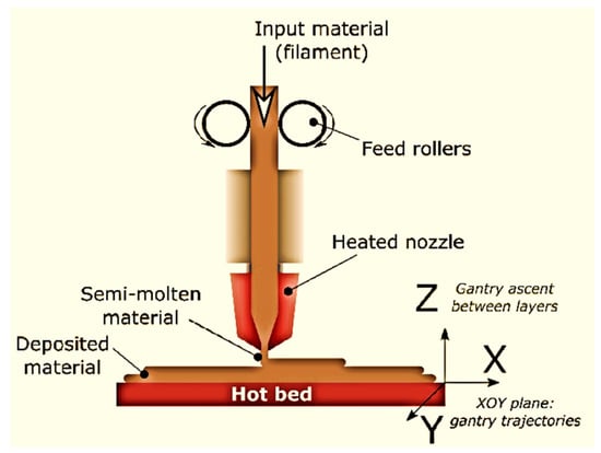
Figure 1. Schematic view of fused filament fabrication (FFF) [44].
The popularity of this method of manufacturing materials today can be attributed to its ease, affordability, non-toxicity, and economic value. Sensors can be incorporated with FFF by stopping the printing process and integrating them inside the enclosure. For embedded piezoelectric accelerometers, Sbriglia et al. physically inserted sensors and stopped the printing process [45]. Monitoring state-of-health and real-time diagnostics are possible with FFF-embedded sensors. To obtain accurate readings and maximum sensitivity, the sensor must be placed at the optimal depth. Using fine-pitch copper mesh and embedded copper wires, Shemelya et al. developed three different types of capacity sensors. These sensors were incorporated into Aerotech’s gantry system [46].
3D printing with FFF technology has shown great promise for producing parts with embedded sensors. A wide range of sensors can be developed using FFF technology, including electrochemical, capacitive, piezoresistive, and piezoelectric sensors. Košir et al. developed a single-process FFF methodology for producing dynamic piezoelectric sensors. The 3D-printed dynamic sensor was made using four different filaments: thermoplastic polyurethane (TPU) (electrode support), heat treat professionals polylactic acid (HTPRO PLA) (build surface), electrify (electrodes), and polyvinylidene fluoride (PVDF) (piezoelectric film). FFF was used to make the piezoelectric sensor using polyvinylidene fluoride (PVDF) and poling with an electric field of 16.5 MV/m. As a result of this technique, two types of piezoelectric sensors were manufactured to measure 31 (in-plane—direction along the print trace) and 32 (in-plane—direction perpendicular to 31). The produced charge and the excitation force were used to measure piezoelectric responses in-plane and out-of-plane. Through FFF, Katseli et al. created an electrochemical cell-on-a-chip device. Using a dual extruder 3D printer, a miniature polylactic acid (PLA) cell was made in a single step with three electrodes embedded in carbon-loaded ABS conductive material (Figure 2).
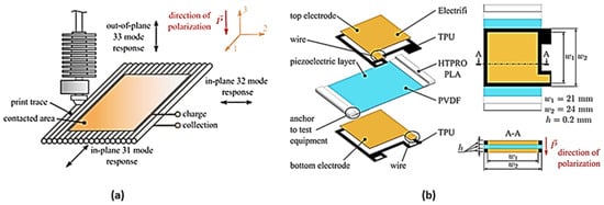
Figure 2. (a) FFF dynamic sensor design in a single process with specified dimensions; (b) for an FFF piezoelectric PVDF film, coordinate the system and mode response directions [46].
The electrochemical sensor is used to test urine contaminated with caffeine (CAF) and paracetamol (PAR) in pharmaceutical pills. Electrolytes with optimal background property and sensitivity for PAR and CAR have been determined to be 0.3 mol/L. A differential pulse voltammetry (DPV) technique was used to measure PAR and CAF simultaneously. Additionally, the design of the electrochemical chip enabled sensitive and quick voltametric analysis using modest amounts of material. In a study by Gooding et al. [47], conductive PLA-graphene composite filaments were used in a 3D-printed strain gauge, which consisted of a rectangular item made with 3DSolutech Natural Clear PLA. In order to measure strain gauge resistance using the conductive material, the bulk resistivity (0.6 cm) and known geometry were used. As soon as the strain gauge is attached to a circuit and supplied with voltage, it deforms and the resistance changes, depending on the geometry and amount of applied stress. When a strain gauge is stressed, the output voltage fluctuation is monitored to determine the sensitivity of the gauge.
An advanced registration technique was developed to capture the moments when the fused deposition modeling machine halted the development of the component, integrated the sensor, and restarted it until the part was completely embedded in polycarbonate material. Wires, meshes, microcontrollers, and light-emitting diodes were embedded as bulk conductive sensors. In order to identify three metallic materials and saltwater from distilled water, these capacitive sensors measured the relative capacitance at ideal depth. Sensors that are embedded in bulk conductive materials are used in biomedical applications, material sensing, electronic characterization, and electrical interconnect characterization. An FDM 3D printer extrudes thermoplastic filament through a nozzle after melting the thermoplastic filament. FDM was first introduced by Crump [48]. In three dimensional (3D) printing, thermoplastic filaments such as polyamide (PA), polylactic acid (PLA), acrylonitrile butadiene styrene (ABS), polycarbonate (PC), etc., are commonly used. Due to its low cost of materials and open-source nature, fused deposition modeling (FDM) has been extensively used, but its slow printing speed and low printing resolution limit its use. 3D printing with FFF/FDM depends on the diameter of the raw materials used to create the object. The two most common standard diameters for materials are 1.75 mm and 2.85 mm, with a few small variations in between. In addition to printing speed, filament extrusion rate, and quantity of material deposited per unit length, the diameter of the raw material influences the printing process. Filament diameter also affects the accuracy and precision of the printed entity [49].
- (ii)
-
Stereolithography (SLA)/digital light projection (DLP)-based embedded sensors
A photopolymerization-based 3D printer consists of four different technologies: polyJet, digital light projection, stereolithography, and two-photon polymerization [50]. Using a UV laser, SLA creates 3D objects by curing resin layer by layer. UV light is exposed using a projector, also known as a digital light processing unit (DLP). Using micronozzles and UV light, PolyJet jets photopolymer resin droplets while simultaneously curing them. In 2PP, two photons are absorbed simultaneously in a photopolymer substance. A trend toward fabricating embedded electrochemical microfluidic devices (EMDs) and micro-electromechanical systems (MEMSs) will emerge in stereolithography (SLA) 3D printing technology. The light-activated resin was cured layer by layer in a vat using directed irradiation [51]. According to Tse et al., SLA can be used to develop high aspect ratio reaction packages directly on top of MEMS devices [52]. An electrode implanted in a microfluid device was developed by Costa et al. using stereolithography (SLA). SLA-printed EMDs were demonstrated to be an appropriate substitute tool for coupling separation procedures. In addition to good electrochemical stability, EMD has a high level of conductive activity. As shown in Figure 3, Ragones et al. used SLA to create a stiff mold that was then used to cast a PDMS chip that served as the biosensor’s substrate.
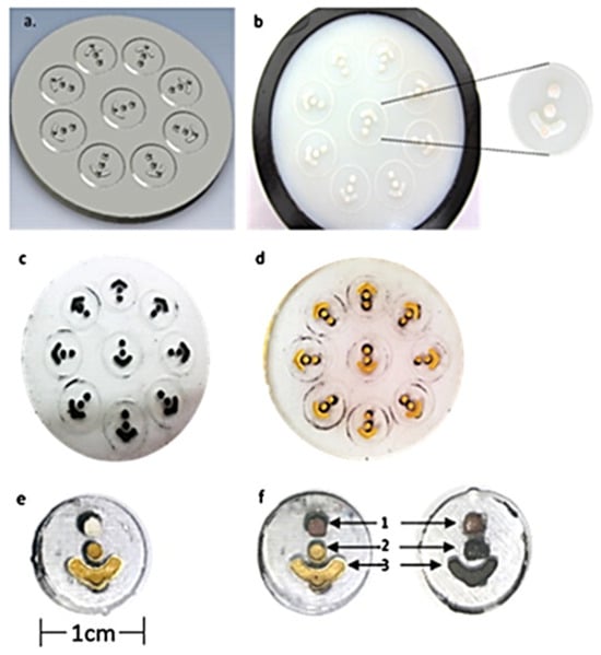
Figure 3. (a) Design with negative molds; (b) with SLA technology, a 3D-printed mold; (c) pits and electrode patterns loaded with conductive ink crafted from PDMS; (d) electrodes upon the sputtering of Au; (e) electrodes upon Au electroplating; (f) chip of Au and carbon [53].
Conductive ink was then poured into the trenches created on the casting using the mold as a guide. Figure 4 and Figure 5 showed the development of tactile sensors via DLP technology, which used conductive ink in printed channels [51]. Hossain et al. also incorporated a flexible RFID temperature memory sensor with no chips into 3D-printed molds [54].
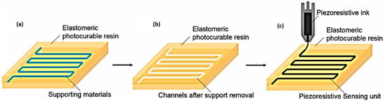
Figure 4. Indirect development of sensors through printed conduits; (a) sensor body in the space of the channels with support material; (b) removal support to create vacant channels; (c) piezoresistive ink injections [46].
Figure 5. Fabrication process of tactile sensor (a) elucidate printing; (b) using microfluidic channels to print on the substrate layer (c) convex structure printing on the cover; (d) sealing and infusing Galinstan [55].
The sensors were produced from many materials at the same time. Initially, a base structure with a microfluidic channel was formed using a photo-sensitive resin substrate. Then, in a resin vat, a distinct photosensitive material was printed to make the channel cover; Figure 5 shows the injection of Galinstan liquid metal into the microchannels following the manufacturing of the 3D-printed part of the sensor. Wang et al. developed 3D-printed functional sensors with incorporated channels through DLP technology, which were injected with Galinstan metal [55].
The applied forces increased successively between 0 N and 10 N under temperatures ranging from 20 °C to 60 °C during the examination of the tactile sensors [55] (Figure 6). Wang et al. also performed 200 cycles with a loading force of 7.5 N and a frequency of 0.08 Hz, lasting 2400 s apiec
Figure 6. Tendencies of tactile sensor: (a) changes in resistance with varying loading factors; (b) resistivity varies with loading frequencies; (c) 200 loading and unloading cycles; (d) testing for heating and cooling cycles [55].
In stereolithography, layers of the model are drawn out or selectively cured using an ultraviolet (UV) laser in a vat of liquid polymer (resin). In this method, a laser beam is aimed across the printing bed using mirrors powered by galvanometers, curing resin point-to-point as it passes. After the first layer is cured, the laser starts curing the next layer, and the printing bed moves up in a top-down system or down in a bottom-up system. It is important to determine the lowest possible laser spot size when determining the resolution of a part. Galvanometer (galvo) systems’ resilience and quality can affect the repeatability and resolution of the process. A printer X, Y resolution is correlated with surface finish, edge details and crispness, minimum feature size, and part tolerance (accuracy and precision). In general, SLA systems can achieve an X, Y resolution of 50 m, a minimum feature size of 150 m, and an overall tolerance of ±100 m, whereas, currently available digital light projection (DLP) systems can typically attain an overall tolerance of ±75 µm, a minimum feature size of 50–100 µm, and an X, Y resolution of 25–50 µm [56][57][58].
- (iii)
-
Direct Ink Writing (DIW)-based embedded sensors
An extrusion group technique called Direct Ink Writing (DIW), often called Robocasting, was typically employed for non-Newtonian viscous slurry with composite rheological qualities, since it prints at room temperature [59]. The software system, which develops the structure, and the output device, which receives the motion instructions to finish the fabrication process, are the two primary components of equipment used in the DIW method. This method has some special advantages; for the creation of embedded sensor technology, it complements other traditional methods (casting, CNC machining, hot pressing, and molding approaches) rather than competing with them, and it can form a hybrid approach [60]. DIW demonstrates great potential for the development of 3D-printed sensors, with superior functional properties. The transformation of materials with solid-like properties into ink can be applied to metals [61], ceramics [62], wood [63]. Researchers using DIW expanded globally, moving beyond the field of structural ceramics into other areas, like 3D bioprinting [64], energy [65], sensors [66], and robots [67], etc. A 3D printing technique that can print many components, including conductors [26], piezoelectric/dielectrics [60], flexible [68], and stiff materials [61], is crucial for the 3D printing of sensors [69] because most sensors tend to consist of multiple types of materials. It is possible to produce high-quality, pliable, and consistently sensitive sensors using printable inks [70]. Layered resistance sensors were created using the direct ink writing technique by Vatani et al. [71]. Carbon nano tube inks were used to create the first 3D-printed sensing arrays. To complete the sensors, the 3D-printed portion was encased in polyethylene terephthalate and photocurable resin. Shi et al. prepared high-resolution 3D direct ink writing strain sensors using polydimethylsiloxane (PDMS) sub-microbeads/graphene oxide nanocomposite inks. Kim et al. directly printed a glove-type sensor with ten strain gauges to measure finger flexion and extension. The result was a small sensor system that could be manufactured quickly [66]. It is possible to create 3D-printed components with features as small as 250 nm using the direct ink writing method [72].
- (iv)
-
Direct Energy Deposition (DED)-based embedded sensors
DED is another AM technology. By scanning a laser beam across a coated targeted surface, a melt pool is generated, and a stream of metallic powder or wire is fed into it (Figure 7) [73]. Polymers, ceramics, and metals comprise some of the material feedstocks employed with DED; however, metals are the most commonly used material in this method, provided as wires or powder [74]. Juhasz et al. introduced a method of printing embedded temperature-resistant strain sensors for metal dog bone specimens using DED [75]. To track temperature degradation and sensor damage, a thick sheet of temperature-resistant material was printed with embedded sensors, and its thickness was adjusted across several trials. One of the main issues that prevented AM embedded sensors from using DED is the protection of the sensor from damage due to laser exposure and temperature changes. The dog bone specimens were 3D printed using a 375 W laser power, 3.23 g/min mass flow rate, 1.7 mm laser spot size, and 1.02 mm layer height. The thickest 3D-printed strain gauge sensor was the only one fabricated through the DED process and could generate an output response when tensile stress was applied.
Figure 7. Illustration of a laser-powered DED process [46].
- (v)
-
Laser powder bed fusion (LPBF)-based embedded sensors
One of the most prevalent AM techniques is laser powder bed fusion (LPBF), in which powder is melted and fused using a laser. A variety of metals, such as Inconel, titanium, and stainless steel, as well as polymers, such as nylon, were typically used [76]. Standardization of LPBF embedding sensors was introduced by Binder et al. [77]. In terms of embedded sensing, LPBF has a few challenges in terms of ensuring a safe environment for the sensor (such as high temperatures, high pressures, powder contamination, chamber dimensions, inert gas flows, and the powder coater). With an elastic casting compound, the PT100 temperature sensor was protected from electrostatics and powder contamination, while maintaining precise measurements. All sensors were operational after embedding, but the delayed reaction was caused by the embedding’s isolative effect. To protect the sensor from direct laser radiation, an aluminum cover was fitted. Stoll et al. introduced innovative non-destructive testing techniques for monitoring SS 316 by utilizing embedded eddy current (EC) sensors [78]. Using embedded ECs, it was demonstrated that crack propagation could be tracked and the extent of the damage assessed over an extended period. Magnetic fields are a mainstay of EC operation principles, which are based on the use of SS 316. This material has a low magnetic permeability, matching EC operation principles that require the use of magnetic fields. The sensor was systematically embedded into the CAD model using the AM process, and after selective laser melting (SLM), the cavity was filled with the sensor. As shown in Figure 8 and Figure 9, the cavity filled with resin after the sensor was pressed against the bottom surface of the cavity for sensor integration. Raw materials in LPBF are typically powders with particle sizes ranging from 10 to 60 microns. LPBF is characterized by a thin layer of powder deposited on a build plate by a spreader [79].
Figure 8. (a) CAD representation of the prototype with a specifically designed cavity for EC sensor integration; (b) schematic diagram of the prototype before crack development; (c) schematic diagram of the prototype depicting crack progression towards the embedded sensor [78].
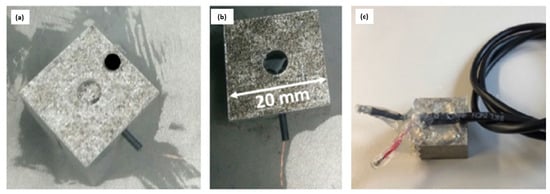
Figure 9. Procedure for integrating EC sensors: (a) removal of powder, placing heat-shrink tubes within protect wires, and passing wires through tubes; (b) cavity incorporation of the EC sensor; (c) specimens for the LPBF with soldered cables [78].
SS 316 embedded sensors were developed by Havermal et al. to compare bare SS 316 samples and measure strain levels, plastic deformation, and elastic deformation [78]. By embedding the sample in the substrate through a groove in the part, nickel-coated Fiber Bragg Grating (FBG) sensors detect the motion of the sample. In the initial cycles, the sample was plastically deformed but not in subsequent cycles. Long-term elastic stability was investigated using the sensor. To minimize sensor response time, H. Hyer and C. Petrie used SS 316 powders to embed an optical sensor and a thermocouple to measure strain. To sense strain, the optical sensor needed nearly perfect embedding, while the embedded thermocouple’s surface roughness and gaps should be minimized [80]. A strain and temperature response is crucial for determining the results. In the embedded region, strain response is well-observed; adequate bonding is also observed. Even though the embedded sensor’s heating rate was different from the bare sensor’s, Figure 10 showed that the embedded sensor reached the same temperature as the bare sensor. Despite having approximately the same amount of noise, embedded and bare sensors share the same vibrational detection accuracy (Figure 11), although bare sensors lack control parameters. Jung et al. described that the IC is Bluetooth-enabled, with a connection range exceeding 100 m.
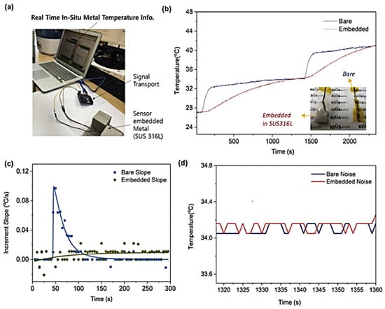
Figure 10. Temperature sensor operation processed by SE-SLM is validated by comparing data with a bare temperature sensor: (a) monitoring the in situ temperature of SE-SLM SUS316L using data reading configuration; (b) comparison of temperatures; (c) curve of temperature increase slope; (d) comparison of noise levels [81].
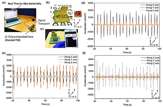
Figure 11. IC component based on PCB embedded in metal: (a) configuration of an IC chip inserted in a metal component; (b) Inconel 718 turbine vane integrated into an IC chip; (c) turbine vane temperature monitored wirelessly; acceleration data recorded for every vibration input axis (d) X-axis, (e) Y-axis, (f) Z-axis [81].
- (vi)
-
Inkjet-based embedded sensors
By using piezoelectric inkjet technology, inkjet 3D printers release material droplets onto a bed; each layer is healed before the next layer is deposited. There are two types of inkjet printing: drop-on-demand printing (DoD) and continuous inkjet printing (CIJ) [82]. These technologies led to the development of two multi-material technologies: polyjet (Stratasys Objet Geometries Co., Rehovot, Israel) (Figure 12a) and multijet (3D Systems) (Figure 12b).
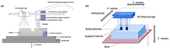
Figure 12. Schematic diagram of (a) multijet; (b) polyjet printing [46].
Both technologies employed micronozzles to jet liquid plastic materials, casting wax materials, or photopolymer resin droplets while simultaneously curing them with UV light [83]. In those technologies, print heads are supported by gel-like materials. Printheads in multijet were limited to two, whereas printheads in polyjet could be two or more. Andà et al. developed a flexible electromagnetic actuator using a low-cost inkjet printer [84][85]. Through additive manufacturing, they built a conductive coil onto a PET substrate and attached an external magnet to it. Additionally, a strain gauge was 3D printed onto the PET beam and connected with a coil and magnet to the patterned printed circuit board. With the help of polyjet technology, Pinto et al. developed a rapid manufacturing method of microfluidic substrates embedded with liquid metals [86][87]. Guo et al. explained a simple method for fabricating microfluid strain sensors widely used in lab-on-chip devices for strain and pressure measurement using inkjet printing [88]. In addition, they explained that 3D printing opened a new era for the development of soft robotic sensors. Microfluidic sensors are made by 3D printing, which reduces the cost of materials and saves time. The goal of this study is to examine the behavior of a mesoscale inkjet-printed accelerometer in the low-frequency domain (up to 20 Hz), which is well-suited for common applications in seismic and human monitoring. Four spring legs hold a polyethylene terephthalate membrane to a fixed support [89]. An inkjet-printed polymeric accelerometer with SU-8 material deposition was described by Roberto et al. The optimized device has a resolution of 2 × 10⁻³ g, a sensitivity of 6745 nm/g, and an acceleration range of 0–0.7 g. Based on these characteristic properties, inkjet printing can be used for a wide range of applications requiring accurate acceleration measurements across small displacements [90]. The low-cost magnetic field sensor prototype was also explained by Bruno et al. A magnetic field range of 0–27 mT, a device responsivity of 3700/T, and a resolution of 0.458 mT were investigated [91]. Commercially available piezo-based inkjet printers have made it possible to print RF structures with 20 m features. Inkjet printers based on electro hydrodynamics can produce features smaller than 1 mm in size [92].
- (vii)
-
Hybrid additive manufacturing technology
The speed at which additive manufacturing produces goods, especially in large quantities, prevents it from being used profitably. As a result, hybrid procedures are concluded by contemporary research, which include the integration of additive processes into the regular industrial production process [93][94][95]. Additive manufacturing requires a repeatable process due to its sequential nature. With liquid metal lattice materials, Deng et al. created re-configurable lattice hands [96]. Combining DLP 3D printing with carbon nanotube (CNT) ultrasonication coating, Yin et al. created a programmable lattice pressure sensor [97]. In stereolithography (SLA) technology and dip coating, Kamat et al. created a piezoresistive pressure sensor containing graphene nanoplatelets [98]. Different metallic and alloy coatings are deposited using electroless plating (ELP), including copper, silver, gold, nickel-phosphorus alloy, etc. A 3D substrate is also a preferred complementary technology for manufacturing 3D electronics in hybrid additive manufacturing [99][100][101]. To determine the ELP deposition area for 3D electronics, Hensleigh et al. used SLA printing to create a dual-material structure using positive, negative, and neutral resins, which were then soaked in positive or negative catalyst solutions [102]. Using DLP and ELP procedures to deposit metal layers on the micro-lattice, Shin et al. increased the lattice’s compressive rigidity from 8.8 MPa to 11.1 MPa [103]. To fabricate high-resolution 3D conformal/embedded circuit boards, sensors, antennas, etc., Liu et al. integrated laser-activated ELP with a variety of AM technologies [104][105][106][107][108].
Table 2. Summary of AM-based 3D printing methods and materials.
| Printing Technology | AM Based 3D Printing Methods | Materials | Performance of Materials | References |
|---|---|---|---|---|
| Extrusion-based printing | Fused deposition modeling (FDM) | Thermoplastics e.g., PLA, ABS, nylon | The filament was melted and extruded through a high-temperature nozzle that was used for 3D translation. | [13] |
| 3D Inkjet | Ultraviolet (UV) curable and low viscous materials | Viscosity is crucial in 3D printing. It affects the quality of the printed object and speed of the printing process. Low viscosity materials require lower extrusion temperatures and fast printing speeds. | [109][110] | |
| Direct ink writing (DIW) | Elastomers, thermosets, metals, and ceramics in micro/nano particle solutions and biomaterials | It can print materials at room temperature and in an ambient environment. Inks were formulated to exhibit shear-thinning and yield rheological behaviors, which are desired to be extruded smoothly and also maintain their shapes after extrusion. | [111][112] | |
| Liquid resin-based printing | Stereolithography (SLA) | Light (UV, LEDs, or laser) curable polymers | To create a solid layer, a UV laser is used to locally cure the resin along the printing routes or projected patterns. SLA uses a point-source laser light beam, but DLP increases printing speed by projecting pictures across the entire platform at each layer. | [113][114] |
| Direct light processing (DLP) | [115] | |||
| Powder-based printing | Selective laser sintering (SLS) | Metal and alloys, polymers, and semiconductors | The particles are locally melted and fused together using a high-energy laser beam to create 3D geometry layer by layer. The platform is lowered after each layer is created, and fresh powder is added to print the subsequent layer. | [116] |
| Direct energy deposition (DED) | For melting wire-based or powder-based filler materials, a high-energy beam is employed. It can be utilized in tandem with other subtractive manufacturing techniques and for repair reasons. | [117] | ||
| Laser powder bed fusion (LPBF) | In it, a laser is used to melt and fuse powder. | [114] |
References
- Dutta, T.; Noushin, T.; Tabassum, S.; Mishra, S.K. Road Map of Semiconductor Metal-Oxide-Based Sensors: A Review. Sensors 2023, 23, 6849.
- Dutta, T.; Ganguly, J.; Sarkar, S. Pico-level DNA sensing by hetero-polymetalate, Na10·80H2O, cluster. Appl. Nanosci. 2018, 8, 1259–1265.
- Dutta, T.; Sarkar, S. Nanocarbon–{2·130H2O} composite to detect toxic food coloring dyes at nanolevel. Appl. Nanosci. 2016, 6, 1191–1197.
- Mishra, A.K.; Mishra, S.K.; Verma, R.K. Doped Single-Wall Carbon Nanotubes in Propagating Surface Plasmon Resonance-Based Fiber Optic Refractive Index Sensing. Plasmonics 2017, 12, 1657–1663.
- Shrivastav, A.M.; Mishra, S.K.; Gupta, B.D. Surface Plasmon Resonance-Based Fiber Optic Sensor for the Detection of Ascorbic Acid Utilizing Molecularly Imprinted Polyaniline Film. Plasmonics 2015, 10, 1853–1861.
- Mishra, A.K.; Mishra, S.K. Gas sensing in Kretschmann configuration utilizing bi-metallic layer of Rhodium-Silver in visible region. Sens. Actuators B Chem. 2016, 237, 969–973.
- Mishra, S.K.; Gupta, B.D. Surface Plasmon Resonance-Based Fiber-Optic Hydrogen Gas Sensor Utilizing Indium–Tin Oxide (ITO) Thin Films. Plasmonics 2012, 7, 627–632.
- Tabassum, S.; Nayemuzzaman, S.; Kala, M.; Kumar Mishra, A.; Mishra, S.K. Metasurfaces for Sensing Applications: Gas, Bio and Chemical. Sensors 2022, 22, 6896.
- Mishra, A.K.; Mishra, S.K.; Gupta, B.D. Gas-Clad Two-Way Fiber Optic SPR Sensor: A Novel Approach for Refractive Index Sensing. Plasmonics 2015, 10, 1071–1076.
- Tetsuka, H.; Shin, S.R. Materials and technical innovations in 3D printing in biomedical applications. J. Mater. Chem. B 2020, 8, 2930–2950.
- Atala, A.; Yoo, J.J. Essentials of 3D Biofabrication and Translation; Academic Press: Cambridge, MA, USA, 2015.
- Additive Manufacturing Standards. Available online: https://www.astm.org/products-services/standards-and-publications/standards/additive-manufacturing-standards.html (accessed on 2 March 2010).
- Ngo, T.D.; Kashani, A.; Imbalzano, G.; Nguyen, K.T.; Hui, D. Additive manufacturing (3D printing): A review of materials, methods, applications and challenges. Compos. Part B Eng. 2018, 143, 172–196.
- Daly, A.C.; Riley, L.; Segura, T.; Burdick, J.A. Hydrogel microparticles for biomedical applications. Nat. Rev. Mater. 2020, 5, 20–43.
- Veidt, M.; Liew, C. Non-destructive evaluation (NDE) of aerospace composites: Structural health monitoring of aerospace structures using guided wave ultrasonics. In Non-Destructive Evaluation (NDE) of Polymer Matrix Composites; Elsevier: Amsterdam, The Netherlands, 2013; pp. 449–479.
- Gokhare, V.; Raut, D.; Shinde, D. A Review paper on 3D-Printing Aspects and Various Processes Used in the 3D-Printing. Int. J. Eng. Tech. Res. 2017, 6, 953–958.
- Attaran, M. The rise of 3-D printing: The advantages of additive manufacturing over traditional manufacturing. Bus. Horiz. 2017, 60, 677–688.
- Pereira, T.; Kennedy, J.V.; Potgieter, J. A comparison of traditional manufacturing vs additive manufacturing, the best method for the job. Procedia Manuf. 2019, 30, 11–18.
- Karayel, E.; Bozkurt, Y. Additive manufacturing method and different welding applications. J. Mater. Res. Technol. 2020, 9, 11424–11438.
- Pérez, M.; Carou, D.; Rubio, E.M.; Teti, R. Current advances in additive manufacturing. Procedia CIRP 2020, 88, 439–444.
- Regis, J.E.; Renteria, A.; Hall, S.E.; Hassan, M.S.; Marquez, C.; Lin, Y. Recent trends and innovation in additive manufacturing of soft functional materials. Materials 2021, 14, 4521.
- Emon, M.O.F.; Alkadi, F.; Philip, D.G.; Kim, D.-H.; Lee, K.-C.; Choi, J.-W. Multi-material 3D printing of a soft pressure sensor. Addit. Manuf. 2019, 28, 629–638.
- Agarwala, S.; Goh, G.L.; Yap, Y.L.; Goh, G.D.; Yu, H.; Yeong, W.Y.; Tran, T.J.S.; Physical, A.A. Development of bendable strain sensor with embedded microchannels using 3D printing. Sens. Actuators A Phys. 2017, 263, 593–599.
- Ota, H.; Emaminejad, S.; Gao, Y.; Zhao, A.; Wu, E.; Challa, S.; Chen, K.; Fahad, H.M.; Jha, A.K.; Kiriya, D. Application of 3D printing for smart objects with embedded electronic sensors and systems. Adv. Mater. Technol. 2016, 1, 1600013.
- Wu, S.-Y.; Yang, C.; Hsu, W.; Lin, L. 3D-printed microelectronics for integrated circuitry and passive wireless sensors. Microsyst. Nanoeng. 2015, 1, 1–9.
- Dijkshoorn, A.; Werkman, P.; Welleweerd, M.; Wolterink, G.; Eijking, B.; Delamare, J.; Sanders, R.; Krijnen, G.J. Embedded sensing: Integrating sensors in 3-D printed structures. J. Sens. Sens. Syst. 2018, 7, 169–181.
- Shrivastav, A.M.; Mishra, S.K.; Gupta, B.D. Localized and propagating surface plasmon resonance based fiber optic sensor for the detection of tetracycline using molecular imprinting. Mater. Res. Express 2015, 2, 035007.
- Mishra, S.K.; Verma, R.K.; Mishra, A.K. Versatile Sensing Structure: GaP/Au/Graphene/Silicon. Photonics 2021, 8, 547.
- Mishra, A.K.; Mishra, S.K.; Singh, A.P. Giant Infrared Sensitivity of Surface Plasmon Resonance-Based Refractive Index Sensor. Plasmonics 2018, 13, 1183–1190.
- López-Higuera, J.M.; Cobo, L.R.; Incera, A.Q.; Cobo, A. Fiber optic sensors in structural health monitoring. J. Light. Technol. 2011, 29, 587–608.
- Deraemaeker, A.; Reynders, E.; De Roeck, G.; Kullaa, J. Vibration-based structural health monitoring using output-only measurements under changing environment. Mech. Syst. Signal Process. 2008, 22, 34–56.
- Di Sante, R. Fibre optic sensors for structural health monitoring of aircraft composite structures: Recent advances and applications. Sensors 2015, 15, 18666–18713.
- Li, H.-N.; Li, D.-S.; Song, G.-B. Recent applications of fiber optic sensors to health monitoring in civil engineering. Eng. Struct. 2004, 26, 1647–1657.
- Amanzadeh, M.; Aminossadati, S.M.; Kizil, M.S.; Rakić, A.D. Recent developments in fibre optic shape sensing. Measurement 2018, 128, 119–137.
- Su, Y.-D.; Preger, Y.; Burroughs, H.; Sun, C.; Ohodnicki, P.R. Fiber optic sensing technologies for battery management systems and energy storage applications. Sensors 2021, 21, 1397.
- Li, C.; Tang, J.; Cheng, C.; Cai, L.; Yang, M. FBG arrays for quasi-distributed sensing: A review. Photonic Sens. 2021, 11, 91–108.
- Luo, P.; Zhang, D.; Wang, L.; Jiang, D. Structural damage detection based on a fiber Bragg grating sensing array and a back propagation neural network: An experimental study. Struct. Health Monit. 2010, 9, 5–11.
- Sieńko, R.; Zych, M.; Bednarski, Ł.; Howiacki, T. Strain and crack analysis within concrete members using distributed fibre optic sensors. Struct. Health Monit. 2019, 18, 1510–1526.
- Cady, W.G. Piezoelectricity: Volume Two: An Introduction to the Theory and Applications of Electromechanical Phenomena in Crystals; Courier Dover Publications: Mineola, NY, USA, 2018.
- Chong, K.P.; Carino, N.J.; Washer, G. Health monitoring of civil infrastructures. Smart Mater. Struct. 2003, 12, 483.
- Baptista, F.G.; Budoya, D.E.; De Almeida, V.A.; Ulson, J.A.C. An experimental study on the effect of temperature on piezoelectric sensors for impedance-based structural health monitoring. Sensors 2014, 14, 1208–1227.
- Qing, X.; Li, W.; Wang, Y.; Sun, H. Piezoelectric transducer-based structural health monitoring for aircraft applications. Sensors 2019, 19, 545.
- Horchidan, N.; Ciomaga, C.; Frunza, R.; Capiani, C.; Galassi, C.; Mitoseriu, L. A comparative study of hard/soft PZT-based ceramic composites. Ceram. Int. 2016, 42, 9125–9132.
- Pranzo, D.; Larizza, P.; Filippini, D.; Percoco, G. Extrusion-Based 3D Printing of Microfluidic Devices for Chemical and Biomedical Applications: A Topical Review. Micromachines 2018, 9, 374.
- Sbriglia, L.R.; Baker, A.M.; Thompson, J.M.; Morgan, R.V.; Wachtor, A.J.; Bernardin, J.D. Embedding sensors in FDM plastic parts during additive manufacturing. In Topics in Modal Analysis & Testing, Volume 10: Proceedings of the 34th IMAC, A Conference and Exposition on Structural Dynamics; Springer: Cham, Switzerland, 2016; pp. 205–214.
- Hassan, M.S.; Zaman, S.; Dantzler, J.Z.R.; Leyva, D.H.; Mahmud, M.S.; Ramirez, J.M.; Gomez, S.G.; Lin, Y. 3D Printed Integrated Sensors: From Fabrication to Applications—A Review. Nanomaterials 2023, 13, 3148.
- Gooding, J.; Fields, T. 3d printed strain gauge geometry and orientation for embedded sensing. In Proceedings of the 58th AIAA/ASCE/AHS/ASC Structures, Structural Dynamics, and Materials Conference, Grapevine, TX, USA, 9–13 January 2017; p. 0350.
- Crump, S.S. Apparatus and Method for Creating Three-Dimensional Objects; United. States patent US 5,121, 329 1992.
- Kantaros, A.; Soulis, E.; Petrescu, F.I.T.; Ganetsos, T. Advanced Composite Materials Utilized in FDM/FFF 3D Printing Manufacturing Processes: The Case of Filled Filaments. Materials 2023, 16, 6210.
- Liu, C.; Huang, N.; Xu, F.; Tong, J.; Chen, Z.; Gui, X.; Fu, Y.; Lao, C. 3D printing technologies for flexible tactile sensors toward wearable electronics and electronic skin. Polymers 2018, 10, 629.
- Hassan, M.S.; Chavez, L.A.; Chou, C.-C.; Hall, S.E.; Tseng, T.-L.; Lin, Y. Mechanical response of shape-recovering metamaterial structures fabricated by additive manufacturing. Mater. Res. Express 2021, 8, 115801.
- Tse, L.; Hesketh, P.; Rosen, D.; Gole, J. Stereolithography on silicon for microfluidics and microsensor packaging. Microsyst. Technol. 2003, 9, 319–323.
- Ragones, H.; Schreiber, D.; Inberg, A.; Berkh, O.; Kósa, G.; Freeman, A.; Shacham-Diamand, Y. Disposable electrochemical sensor prepared using 3D printing for cell and tissue diagnostics. Sens. Actuators B Chem. 2015, 216, 434–442.
- Hossain, S.D.; Mora, M.A.P.; Arif, A.; Lohani, B.; Roberts, R.C. Flexible Chipless RFID Temperature Memory Sensor. In Proceedings of the 2022 IEEE International Conference on Flexible and Printable Sensors and Systems (FLEPS), Vienna, Austria, 10–13 July 2022; pp. 1–4.
- Wang, Y.; Jin, J.; Lu, Y.; Mei, D. 3D printing of liquid metal based tactile sensor for simultaneously sensing of temperature and forces. Int. J. Smart Nano Mater. 2021, 12, 269–285.
- Christina, S.; Deepak, M.K. Stereolithography. In 3D Printing; Dragan, C., Ed.; IntechOpen: Rijeka, Croatia, 2018; pp. 1–22.
- Ertugrul, I.; Ulkir, O.; Ersoy, S.; Ragulskis, M. Additive Manufactured Strain Sensor Using Stereolithography Method with Photopolymer Material. Polymers 2023, 15, 991.
- Ge, Q.; Li, Z.; Wang, Z.; Kowsari, K.; Zhang, W.; He, X.; Zhou, J.; Fang, N.X. Projection micro stereolithography based 3D printing and its applications. Int. J. Extrem. Manuf. 2020, 2, 022004.
- Shahzad, A.; Lazoglu, I. Direct ink writing (DIW) of structural and functional ceramics: Recent achievements and future challenges. Compos. Part B Eng. 2021, 225, 109249.
- Renteria, A.; Balcorta, V.H.; Marquez, C.; Rodriguez, A.A.; Renteria-Marquez, I.; Regis, J.; Wilburn, B.; Patterson, S.; Espalin, D.; Tseng, T.-L.B. Direct ink write multi-material printing of PDMS-BTO composites with MWCNT electrodes for flexible force sensors. Flex. Print. Electron. 2022, 7, 015001.
- Skylar-Scott, M.A.; Gunasekaran, S.; Lewis, J.A. Laser-assisted direct ink writing of planar and 3D metal architectures. Proc. Natl. Acad. Sci. USA 2016, 113, 6137–6142.
- Revelo, C.F.; Colorado, H.A. 3D printing of kaolinite clay ceramics using the Direct Ink Writing (DIW) technique. Ceram. Int. 2018, 44, 5673–5682.
- Rosenthal, M.; Henneberger, C.; Gutkes, A.; Bues, C.-T. Liquid Deposition Modeling: A promising approach for 3D printing of wood. Eur. J. Wood Wood Prod. 2018, 76, 797–799.
- Lee, A.; Hudson, A.; Shiwarski, D.; Tashman, J.; Hinton, T.; Yerneni, S.; Bliley, J.; Campbell, P.; Feinberg, A. 3D bioprinting of collagen to rebuild components of the human heart. Science 2019, 365, 482–487.
- Wei, T.S.; Ahn, B.Y.; Grotto, J.; Lewis, J.A. 3D printing of customized Li-ion batteries with thick electrodes. Adv. Mater. 2018, 30, 1703027.
- Kim, S.; Oh, J.; Jeong, D.; Park, W.; Bae, J. Consistent and reproducible direct ink writing of eutectic gallium–indium for high-quality soft sensors. Soft Robot. 2018, 5, 601–612.
- Wehner, M.; Truby, R.L.; Fitzgerald, D.J.; Mosadegh, B.; Whitesides, G.M.; Lewis, J.A.; Wood, R.J. An integrated design and fabrication strategy for entirely soft, autonomous robots. Nature 2016, 536, 451–455.
- Kumar, A.J.S.; Research, B.-S. Flexible and wearable capacitive pressure sensor for blood pressure monitoring. Sens. Bio-Sens. Res. 2021, 33, 100434.
- Schouten, M.; Wolterink, G.; Dijkshoorn, A.; Kosmas, D.; Stramigioli, S.; Krijnen, G. A review of extrusion-based 3D printing for the fabrication of electro-and biomechanical sensors. IEEE Sens. J. 2020, 21, 12900–12912.
- Hassan, M.S.; Zaman, S.; Rodriguez, A.; Molina, L.; Dominguez, C.E.; Morgan, R.; Bernardin, J.; Lin, Y. Direct ink write 3D printing of wave propagation sensor. Flex. Print. Electron. 2022, 7, 045011.
- Vatani, M.; Engeberg, E.D.; Choi, J.-W. Conformal direct-print of piezoresistive polymer/nanocomposites for compliant multi-layer tactile sensors. Addit. Manuf. 2015, 7, 73–82.
- Chakraborty, P.K. Chapter 5—3D printing of 2D nano-inks for multifarious applications. In Smart Multifunctional Nano-Inks; Gupta, R.K., Nguyen, T.A., Eds.; Elsevier: Amsterdam, The Netherlands, 2023; pp. 91–124.
- Carlota, V. The Complete Guide to Directed Energy Deposition (DED) in 3D Printing. Available online: https://www.3dnatives.com/en/directed-energy-deposition-ded-3d-printing-guide-100920194 (accessed on 10 September 2019).
- Gibson, I.; Rosen, D.; Stucker, B.; Gibson, I.; Rosen, D.; Stucker, B. Directed energy deposition processes. In Additive Manufacturing Technologies: 3D Printing, Rapid Prototyping, Direct Digital Manufacturing; Springer: New York, NY, USA, 2015; pp. 245–268.
- Juhasz, M.; Tiedemann, R.; Dumstorff, G.; Walker, J.; Du Plessis, A.; Conner, B.; Lang, W.; MacDonald, E. Hybrid directed energy deposition for fabricating metal structures with embedded sensors. Addit. Manuf. 2020, 35, 101397.
- Hyer, H.C.; Carver, K.; List, F.A., III; Petrie, C.M. Embedding Sensors in 3D Printed Metal Structures; Oak Ridge National Lab.(ORNL): Oak Ridge, TN, USA, 2021.
- Havermann, D.; Mathew, J.; Macpherson, W.N.; Maier, R.R.; Hand, D.P. In-situ strain sensing with fiber optic sensors embedded into stainless steel 316. In Proceedings of the Sensors and Smart Structures Technologies for Civil, Mechanical, and Aerospace Systems, San Diego, CA, USA, 8–12 March 2015; pp. 852–859.
- Stoll, P.; Gasparin, E.; Spierings, A.; Wegener, K. Embedding eddy current sensors into LPBF components for structural health monitoring. Prog. Addit. Manuf. 2021, 6, 445–453.
- Habiba, U.; Hebert, R.J. Powder Spreading Mechanism in Laser Powder Bed Fusion Additive Manufacturing: Experiments and Computational Approach Using Discrete Element Method. Materials 2023, 16, 2824.
- Hyer, H.; Petrie, C. Embedding Sensors in Stainless Steel using Laser Powder Bed Fusion; Oak Ridge National Lab. (ORNL): Oak Ridge, TN, USA, 2022.
- Jung, I.D.; Lee, M.S.; Lee, J.; Sung, H.; Choe, J.; Son, H.J.; Yun, J.; Kim, K.-b.; Kim, M.; Lee, S.W.; et al. Embedding sensors using selective laser melting for self-cognitive metal parts. Addit. Manuf. 2020, 33, 101151.
- Al-Halhouli, A.; Qitouqa, H.; Alashqar, A.; Abu-Khalaf, J. Inkjet printing for the fabrication of flexible/stretchable wearable electronic devices and sensors. Sens. Rev. 2018, 38, 438–452.
- Piłczyńska, K. Chapter 8—Material jetting. In Polymers for 3D Printing, Izdebska-Podsiadły, J., Ed.; William Andrew Publishing: Norwich, NY, USA, 2022; pp. 91–103.
- Ando, B.; Marletta, V. An all-inkjet printed bending actuator with embedded sensing feature and an electromagnetic driving mechanism. Actuators 2016, 5, 21.
- Njogu, P.M.; Sanz-Izquierdo, B.; Jun, S.Y.; Kalman, G.; Gao, S.; Malas, A.; Gibbons, G.J. Evaluation of planar inkjet-printed antennas on a low-cost origami flapping robot. IEEE Access 2020, 8, 164103–164113.
- Shi, Y.; Ye, P.; Yang, K.; Meng, J.; Guo, J.; Pan, Z.; Bayin, Q.; Zhao, W. Application of microfluidics in immunoassay: Recent advancements. J. Healthc. Eng. 2021, 2021, 2959843.
- Fumeaux, N.F. Additive and Digital Manufacturing of Transient Sensors and Bioelectronics; EPFL: Lausanne, Switzerland, 2023.
- Goh, G.L.; Agarwala, S.; Yong, W.Y. 3D printing of microfludic sensor for soft robots: A preliminary study in design and fabrication. In Proceedings of the 2nd International Conference on Progress in Additive Manufacturing (Pro-AM 2016 singapore); 2016; pp. 177–181. Available online: https://hdl.handle.net/10356/84409 (accessed on 1 February 2024).
- Andò, B.; Baglio, S.; Lombardo, C.O.; Marletta, V.; Pistorio, A. A Low-Cost Accelerometer Developed by Inkjet Printing Technology. IEEE Trans. Instrum. Meas. 2016, 65, 1242–1248.
- Bernasconi, R.; Invernizzi, G.P.; Stampino, E.G.; Gotti, R.; Gatti, D.; Magagnin, L. Printing MEMS: Application of Inkjet Techniques to the Manufacturing of Inertial Accelerometers. Micromachines 2023, 14, 2082.
- Andò, B.; Baglio, S.; Crispino, R.; Marletta, V. Polymeric Transducers: An Inkjet Printed B-Field Sensor with Resistive Readout Strategy. Sensors 2019, 19, 5318.
- Cui, Y.; Nauroze, S.A.; Tentzeris, M.M. 13—Origami-inspired 4D tunable RF and wireless structures and modules. In Smart Materials in Additive Manufacturing; Bodaghi, M., Zolfagharian, A., Eds.; Elsevier: Amsterdam, The Netherlands, 2022; pp. 347–385.
- Bernasconi, R.; Hatami, D.; Hosseinabadi, H.N.; Zega, V.; Corigliano, A.; Suriano, R.; Levi, M.; Langfelder, G.; Magagnin, L. Hybrid additive manufacturing of a piezopolymer-based inertial sensor. Addit. Manuf. 2022, 59, 103091.
- Jeong, H.; Cui, Y.; Tentzeris, M.M.; Lim, S. Hybrid (3D and inkjet) printed electromagnetic pressure sensor using metamaterial absorber. Addit. Manuf. 2020, 35, 101405.
- Materon, E.M.; Wong, A.; Gomes, L.M.; Ibáñez-Redín, G.; Joshi, N.; Oliveira, O.N.; Faria, R.C. Combining 3D printing and screen-printing in miniaturized, disposable sensors with carbon paste electrodes. J. Mater. Chem. C 2021, 9, 5633–5642.
- Deng, F.; Nguyen, Q.-K.; Zhang, P. Multifunctional liquid metal lattice materials through hybrid design and manufacturing. Addit. Manuf. 2020, 33, 101117.
- Yin, Y.M.; Li, H.Y.; Xu, J.; Zhang, C.; Liang, F.; Li, X.; Jiang, Y.; Cao, J.W.; Feng, H.F.; Mao, J.N. Facile fabrication of flexible pressure sensor with programmable lattice structure. ACS Appl. Mater. Interfaces 2021, 13, 10388–10396.
- Kamat, A.M.; Kottapalli, A.G.P. 3D printed graphene-coated flexible lattice as piezoresistive pressure sensor. In Proceedings of the 2021 21st International Conference on Solid-State Sensors, Actuators and Microsystems (Transducers), Orlando, FL, USA, 20–24 June 2021; IEEE: Piscataway, NJ, USA, 2021; pp. 888–891.
- Ashkenazi, D.; Inberg, A.; Shacham-Diamand, Y.; Stern, A. Gold, silver, and electrum electroless plating on additively manufactured laser powder-bed fusion AlSi10Mg parts: A review. Coatings 2021, 11, 422.
- Ghosh, S. Electroless copper deposition: A critical review. Thin Solid Film. 2019, 669, 641–658.
- Peng, X.; Kuang, X.; Roach, D.J.; Wang, Y.; Hamel, C.M.; Lu, C.; Qi, H.J. Integrating digital light processing with direct ink writing for hybrid 3D printing of functional structures and devices. Addit. Manuf. 2021, 40, 101911.
- Hensleigh, R.; Cui, H.; Xu, Z.; Massman, J.; Yao, D.; Berrigan, J.; Zheng, X. Charge-programmed three-dimensional printing for multi-material electronic devices. Nat. Electron. 2020, 3, 216–224.
- Shin, C.S.; Chang, Y.C. Fabrication and Compressive Behavior of a Micro-Lattice Composite by High Resolution DLP Stereolithography. Polymers 2021, 13, 785.
- He, L.; Wang, P.; Yang, J.; Fan, K.; Zhang, H.; Zhang, L.; Jiang, M.; Chen, X.; Chen, Z.; Chen, M.; et al. Smart Lattice Structures with Self-Sensing Functionalities via Hybrid Additive Manufacturing Technology. Micromachines 2024, 15, 2.
- Wang, P.; Li, J.; Deng, L.; Liu, S.; Wang, G.; Huang, J.; Tang, X.; Han, L. Laser-Activated Selective Electroless Plating on 3D Structures via Additive Manufacturing for Customized Electronics. Adv. Mater. Technol. 2023, 8, 2300516.
- Wang, P.; Li, J.; Wang, G.; Hai, Y.; He, L.; Yu, Y.; Wang, X.; Chen, M.; Xu, B. Selectively metalizable low-temperature cofired ceramic for three-dimensional electronics via hybrid additive manufacturing. ACS Appl. Mater. Interfaces 2022, 14, 28060–28073.
- Wang, P.; Li, J.; Wang, G.; He, L.; Yang, J.; Zhang, C.; Han, Z.; Yan, Y. Hybrid additive manufacturing based on vat photopolymerization and laser-activated selective metallization for three-dimensional conformal electronics. Addit. Manuf. 2023, 63, 103388.
- Wang, P.; Li, J.; Yang, J.; Wang, G.; He, L.; Zhang, H. Enabling 3D multilayer electronics through the hybrid of vat photopolymerization and laser-activated selective metallization. Addit. Manuf. 2023, 74, 103717.
- Saleh, E.; Woolliams, P.; Clarke, B.; Gregory, A.; Greedy, S.; Smartt, C.; Wildman, R.; Ashcroft, I.; Hague, R.; Dickens, P.; et al. 3D inkjet-printed UV-curable inks for multi-functional electromagnetic applications. Addit. Manuf. 2017, 13, 143–148.
- Zhao, P.; He, Y.; Trindade, G.F.; Baumers, M.; Irvine, D.J.; Hague, R.J.M.; Ashcroft, I.A.; Wildman, R.D. Modelling the influence of UV curing strategies for optimisation of inkjet based 3D printing. Mater. Des. 2021, 208, 109889.
- Cesarano, J. A review of robocasting technology. MRS Online Proc. Libr. 1998, 542, 133.
- M’barki, A.; Bocquet, L.; Stevenson, A. Linking rheology and printability for dense and strong ceramics by direct ink writing. Sci. Rep. 2017, 7, 6017.
- Tumbleston, J.R.; Shirvanyants, D.; Ermoshkin, N.; Janusziewicz, R.; Johnson, A.R.; Kelly, D.; Chen, K.; Pinschmidt, R.; Rolland, J.P.; Ermoshkin, A. Continuous liquid interface production of 3D objects. Science 2015, 347, 1349–1352.
- Sun, C.; Fang, N.; Wu, D.; Zhang, X. Projection micro-stereolithography using digital micro-mirror dynamic mask. Sens. Actuators A Phys. 2005, 121, 113–120.
- Hull, C.W. Apparatus for Production of Three-Dimensional Objects by Stereolithography. United States Patent 638905, 1984.
- Duda, T.; Raghavan, L.V. 3D metal printing technology. IFAC-Pap. 2016, 49, 103–110.
- Dass, A.; Moridi, A. State of the art in directed energy deposition: From additive manufacturing to materials design. Coatings 2019, 9, 418.
More
Information
Subjects:
Engineering, Industrial
Contributors
MDPI registered users' name will be linked to their SciProfiles pages. To register with us, please refer to https://encyclopedia.pub/register
:
View Times:
2.5K
Revisions:
3 times
(View History)
Update Date:
11 Jun 2024
Table of Contents


Notice
You are not a member of the advisory board for this topic. If you want to update advisory board member profile, please contact office@encyclopedia.pub.
OK
Confirm
Only members of the Encyclopedia advisory board for this topic are allowed to note entries. Would you like to become an advisory board member of the Encyclopedia?
Yes
No
${ textCharacter }/${ maxCharacter }
Submit
Cancel
Back
Comments
${ item }
|
${ item.createdUser.fullName }
${ item.createdAt }
${ item.vote }
${ item.reply }
Delete
${ reply.createdUser.fullName }
${ reply.createdAt }
${ reply.vote }
Delete
There is no reply to this comment~
${ item.replyTextCharacter }/${ item.replyMaxCharacter }
Submit
Cancel
More
No more~
There is no comment~
${ textCharacter }/${ maxCharacter }
Submit
Cancel
${ selectedItem.replyTextCharacter }/${ selectedItem.replyMaxCharacter }
Submit
Cancel
Confirm
Are you sure to Delete?
Yes
No