Your browser does not fully support modern features. Please upgrade for a smoother experience.
Please note this is a comparison between Version 1 by Satyendra Kumar Mishra and Version 3 by Dean Liu.
Embedded sensors (ESs) are used in smart materials to enable continuous and permanent measurements of their structural integrity, while sensing technology involves developing sensors, sensory systems, or smart materials that monitor a wide range of properties of materials. Incorporating 3D-printed sensors into hosting structures has grown in popularity because of improved assembly processes, reduced system complexity, and lower fabrication costs. 3D-printed sensors can be embedded into structures and attached to surfaces through two methods: attaching to surfaces or embedding in 3D-printed sensors.
- embedded sensors
- 3D printing
- inkjet based embedded sensors
- sensing mechanism
1. Introduction
Developing sensors, sensory systems, or smart materials is the focus of sensing technology [1][2][3][4][5][6][7][8][9][1,2,3,4,5,6,7,8,9]. An embedded sensor (ES) provides continuous and enduring measurements of a structure’s structural integrity in smart materials. The integration of ESs was limited to the processing technology used to implant the sensor, although they were sensitive in high temperatures and might be damaged. With streamlined assembly processes, reduced system complexity, and cheaper fabrication costs, 3D-printed sensors are gaining popularity within hosting structures. Two methods can be used to integrate sensors: attaching them to surfaces or embedding them in structures. The first 3D-printed object was created by Hull in 1989 using Stereolithography (SLA). A number of fields, including engineering, manufacturing, biology, and science, have also approved 3D printing. With the development of additive manufacturing, researchers have been able to construct 3D objects with intricate features that were difficult to produce using traditional fabrication techniques. In recent years, embedded 3D printing, an additive manufacturing technique based on material extrusion, has gained a great deal of popularity [10][11][10,11]. As opposed to other printing strategies based on the American Society of Testing Materials (ASTM) standard [12], this printing method allows nozzles to print directly onto “support material” [13]. In contrast to the existing material extrusion process, the new process uses a support matrix with rheological characteristics as the printing medium instead of air. Because shear stress stimulation can break non-covalent and reversible bonds, direct writing can be achieved. When the stimulation is withdrawn and the tip crosses the medium, the medium instantly restores the bond, resulting in ink covering the support material instantly. A support matrix suspends the printed ink due to its rheological characteristics [14]. The hanging structure barely needs assistance before printing. Embedded 3D printing could be support-free, unlike stereolithography and fused deposition modeling. Embedded sensors are a network of devices that are integrated directly into a material. Incorporating them into a host material or physically embedding them is an option [15]. Embedding sensors presents some challenges, including shifts in stress concentrations, crack formation, and increased matrix stiffness, but because the sensors are protected from the external environment, they are less likely to be damaged and more likely to last. In surface-bonded sensors, adhesive is used to attach them to the surface of the host structure. A carefully prepared surface is required to ensure the bonding layer is scaled appropriately to secure the sensor efficiently. There may be a drawback to surface-bonded sensors when it comes to their ability to sense and generate a signal through the bonding layer. This process involves depositing material layer by layer to build a three-dimensional (3D) item from a digital model, known as additive manufacturing (AM), sometimes also called rapid prototyping or 3D printing [16]. Additive manufacturing (AM) has become increasingly popular over the years as a result of its numerous advantages over traditional manufacturing techniques. Compared to conventional methods such as injection molding, plastic forming, CNC machining, and joining plastic, AM technology offers a number of advantages. A number of factors contribute to these advantages, including production cost, speed, quality, and reliability [17][18][17,18]. 3D printing is significantly less expensive than conventional technology for small-volume manufacturing where mold development is expensive. In addition to shortening time to market, it ensures quick prototyping and manufacturing. It promotes customization, personalization, and design imagination. In comparison with other manufacturing technologies, additive manufacturing or 3D printing constantly evolves to increase its advantages and benefits [19][20][21][19,20,21]. Without the correct connection between electrically conductive materials (the communication component) and functional materials (the sensing component), embedded sensing would not work. Multi-material printing enables a fully functional sensor to be fabricated in one step. In comparison with traditional manufacturing methods, which require multiple steps to produce a single sensor and integrate it into a structure, this method was highly advantageous. Unlike conventional technologies, it allowed for a great deal of freedom when it came to developing accessible sensors. AM offers unique advantages over traditional fabrication methods (such as hot pressing, molding, and CNC machines), so it is more likely to be used alongside other techniques than compete against them. It is currently possible to integrate conductive components and functional materials in various ways to facilitate sensing capabilities via additive manufacturing. Combining 3D printing with traditional wiring, printed circuit boards and sensors can be printed [22]. Conductor infusion is another technique that uses 3D printing to print channels in otherwise non-conductive sensing materials and then infuse conductive inks into them [23][24][25][23,24,25]. Co-printing conductors, or conductive materials, in the same cycle as dielectric materials is one of the most desirable and positive aspects of 3D printing technology [26].
2. Approaches to Form Embedded Sensors
Throughout the past few decades, embedded sensors have been studied in structural components, and they have proven to be a dominant technology. However, there are other technologies available, such as fiber optic sensors (FOSs) and piezoelectric sensors (PSs), which are commonly used to develop embedded sensors.- (a)
-
Fiber Optic Sensors (FOSs)For large structures, distributed fiber optic systems are ideal since all fiber optic segments serve as sensors and can measure disturbances inside different areas of the structure. Since this type of sensor relies on modulating light intensity, cracks or other localized structural problems can cause variations in light intensity. There are two important distributed sensor approaches: Optical Time Domain Reflectometry (OTDR) and Brillouin dispersion. Researchers use Rayleigh and Fresnel dispersions and OTDR to monitor structural disturbances. In contrast, Brillouin dispersion displays a measurement-related Doppler shift in light frequency. As distributed sensors have poor resolutions, weak signals, and complex demodulation algorithms, they have not yet seen widespread adoption in civil structures. Despite their innate distributive nature, they have a lot of potential for civil engineering if their challenges are addressed [33][38][33,38]. Recent research has explored the use of FOSs in composites and specific metallic components, especially those with low melting points. Fiber optic sensors should be included in these types of structures in a simpler way, in the interest of advancing science.Table 1.Types of optic fiber sensors.
Point Sensor Quasi-Distributed Sensor Distributed Sensor Sensors Fabry–Perot Cavity
Fiber Bragg Grating
Long gage sensorFiber Bragg Grating Raman/Rayleigh
BrillouinMeasurands Strain (displacement,
pressure, temperature)Strain (displacement, acceleration, pressure, relative fissure, inclination, etc.) Temperature/Strain Modulation Method Phase-modulated optical
fiber sensors or interferometersWavelength Intensity The refractive index of an optical fiber with a single mode is modulated permanently and periodically by a Bragg grating. Since it is a quasi-distributed sensor—a Bragg reflector that can reflect light wavelengths while transmitting others—the Fiber Bragg Gratings (FBG) sensor can be multiplexed easily to monitor voltages at multiple locations at the same time. The dielectric wavelength mirror is created by periodically varying the refractive index of the fiber core. Changes in local temperature or voltage affect the wave period and core refraction index, which are followed by measurable changes in the wavelength of reflected light. There are several significant issues raised by the selection of Fiber Bragg Gratings and the monitoring systems that accompany them. As an example, the spectral overlap of gratings modifies nearby wavelengths. Insufficient light or sidebands at the measured wavelength can also lead to errors in the system [30][32][34][35][36][37][30,32,34,35,36,37].- (b)
-
Piezoelectric Sensors(PSs)
3. Embedded Sensors with 3D Printing Technology
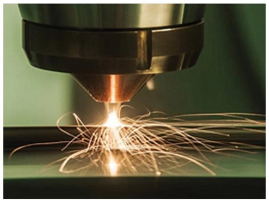
Various additive manufacturing (AM)/3D printing techniques, like ultrasonic AM, laser powder bed fusion (LPBF), laser cladding (LC), stereolithography (SLA), and fused filament fabrication (FFF), are utilized to investigate embedded sensors. Table 2 summarizes various AM-based 3D printing methods.- (i)
-
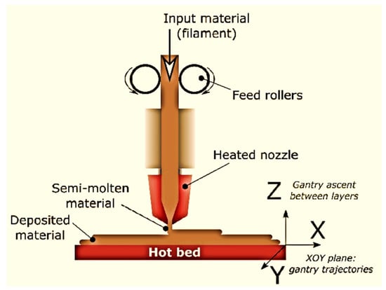
Fused filament fabrication (FFF)/Fused deposition modeling (FDM)-based embedded sensorsThe electrochemical sensor is used to test urine contaminated with caffeine (CAF) and paracetamol (PAR) in pharmaceutical pills. Electrolytes with optimal background property and sensitivity for PAR and CAR have been determined to be 0.3 mol/L. A differential pulse voltammetry (DPV) technique was used to measure PAR and CAF simultaneously. Additionally, the design of the electrochemical chip enabled sensitive and quick voltametric analysis using modest amounts of material. In a study by Gooding et al. [47], conductive PLA-graphene composite filaments were used in a 3D-printed strain gauge, which consisted of a rectangular item made with 3DSolutech Natural Clear PLA. In order to measure strain gauge resistance using the conductive material, the bulk resistivity (0.6 cm) and known geometry were used. As soon as the strain gauge is attached to a circuit and supplied with voltage, it deforms and the resistance changes, depending on the geometry and amount of applied stress. When a strain gauge is stressed, the output voltage fluctuation is monitored to determine the sensitivity of the gauge. An advanced registration technique was developed to capture the moments when the fused deposition modeling machine halted the development of the component, integrated the sensor, and restarted it until the part was completely embedded in polycarbonate material. Wires, meshes, microcontrollers, and light-emitting diodes were embedded as bulk conductive sensors. In order to identify three metallic materials and saltwater from distilled water, these capacitive sensors measured the relative capacitance at ideal depth. Sensors that are embedded in bulk conductive materials are used in biomedical applications, material sensing, electronic characterization, and electrical interconnect characterization. An FDM 3D printer extrudes thermoplastic filament through a nozzle after melting the thermoplastic filament. FDM was first introduced by Crump [48]. In three dimensional (3D) printing, thermoplastic filaments such as polyamide (PA), polylactic acid (PLA), acrylonitrile butadiene styrene (ABS), polycarbonate (PC), etc., are commonly used. Due to its low cost of materials and open-source nature, fused deposition modeling (FDM) has been extensively used, but its slow printing speed and low printing resolution limit its use. 3D printing with FFF/FDM depends on the diameter of the raw materials used to create the object. The two most common standard diameters for materials are 1.75 mm and 2.85 mm, with a few small variations in between. In addition to printing speed, filament extrusion rate, and quantity of material deposited per unit length, the diameter of the raw material influences the printing process. Filament diameter also affects the accuracy and precision of the printed entity [49].
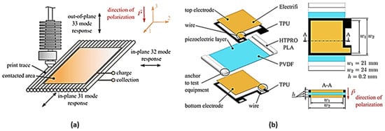 Figure 23. (a) FFF dynamic sensor design in a single process with specified dimensions; (b) for an FFF piezoelectric PVDF film, coordinate the system and mode response directions [46].
- (ii)
-
Stereolithography (SLA)/digital light projection (DLP)-based embedded sensorsConductive ink was then poured into the trenches created on the casting using the mold as a guide. Figure 45 and Figure 56 showed the development of tactile sensors via DLP technology, which used conductive ink in printed channels [51]. Hossain et al. also incorporated a flexible RFID temperature memory sensor with no chips into 3D-printed molds [54].
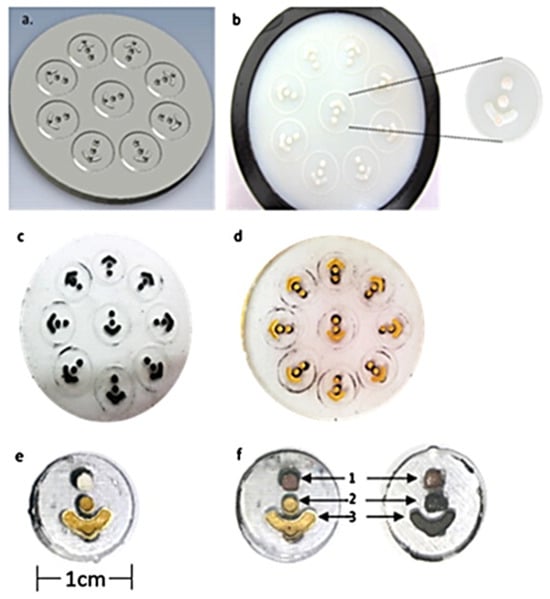 Figure 34. (a) Design with negative molds; (b) with SLA technology, a 3D-printed mold; (c) pits and electrode patterns loaded with conductive ink crafted from PDMS; (d) electrodes upon the sputtering of Au; (e) electrodes upon Au electroplating; (f) chip of Au and carbon [53].
 Figure 45. Indirect development of sensors through printed conduits; (a) sensor body in the space of the channels with support material; (b) removal support to create vacant channels; (c) piezoresistive ink injections [46].The sensors were produced from many materials at the same time. Initially, a base structure with a microfluidic channel was formed using a photo-sensitive resin substrate. Then, in a resin vat, a distinct photosensitive material was printed to make the channel cover; Figure 56 shows the injection of Galinstan liquid metal into the microchannels following the manufacturing of the 3D-printed part of the sensor. Wang et al. developed 3D-printed functional sensors with incorporated channels through DLP technology, which were injected with Galinstan metal [55]. The applied forces increased successively between 0 N and 10 N under temperatures ranging from 20 °C to 60 °C during the examination of the tactile sensors [55] (Figure 67). Wang et al. also performed 200 cycles with a loading force of 7.5 N and a frequency of 0.08 Hz, lasting 2400 s apiec
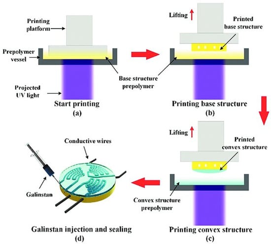 Figure 56. Fabrication process of tactile sensor (a) elucidate printing; (b) using microfluidic channels to print on the substrate layer (c) convex structure printing on the cover; (d) sealing and infusing Galinstan [55].In stereolithography, layers of the model are drawn out or selectively cured using an ultraviolet (UV) laser in a vat of liquid polymer (resin). In this method, a laser beam is aimed across the printing bed using mirrors powered by galvanometers, curing resin point-to-point as it passes. After the first layer is cured, the laser starts curing the next layer, and the printing bed moves up in a top-down system or down in a bottom-up system. It is important to determine the lowest possible laser spot size when determining the resolution of a part. Galvanometer (galvo) systems’ resilience and quality can affect the repeatability and resolution of the process. A printer X, Y resolution is correlated with surface finish, edge details and crispness, minimum feature size, and part tolerance (accuracy and precision). In general, SLA systems can achieve an X, Y resolution of 50 m, a minimum feature size of 150 m, and an overall tolerance of ±100 m, whereas, currently available digital light projection (DLP) systems can typically attain an overall tolerance of ±75 µm, a minimum feature size of 50–100 µm, and an X, Y resolution of 25–50 µm [56][57][58][56,57,58].
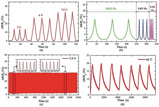 Figure 67. Tendencies of tactile sensor: (a) changes in resistance with varying loading factors; (b) resistivity varies with loading frequencies; (c) 200 loading and unloading cycles; (d) testing for heating and cooling cycles [55].
- (iii)
-
Direct Ink Writing (DIW)-based embedded sensors
- (iv)
-
Direct Energy Deposition (DED)-based embedded sensors
- (v)
-
Laser powder bed fusion (LPBF)-based embedded sensors
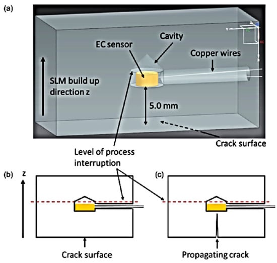 Figure 89. (a) CAD representation of the prototype with a specifically designed cavity for EC sensor integration; (b) schematic diagram of the prototype before crack development; (c) schematic diagram of the prototype depicting crack progression towards the embedded sensor [78].SS 316 embedded sensors were developed by Havermal et al. to compare bare SS 316 samples and measure strain levels, plastic deformation, and elastic deformation [78]. By embedding the sample in the substrate through a groove in the part, nickel-coated Fiber Bragg Grating (FBG) sensors detect the motion of the sample. In the initial cycles, the sample was plastically deformed but not in subsequent cycles. Long-term elastic stability was investigated using the sensor. To minimize sensor response time, H. Hyer and C. Petrie used SS 316 powders to embed an optical sensor and a thermocouple to measure strain. To sense strain, the optical sensor needed nearly perfect embedding, while the embedded thermocouple’s surface roughness and gaps should be minimized [80]. A strain and temperature response is crucial for determining the results. In the embedded region, strain response is well-observed; adequate bonding is also observed. Even though the embedded sensor’s heating rate was different from the bare sensor’s, Figure 110 showed that the embedded sensor reached the same temperature as the bare sensor. Despite having approximately the same amount of noise, embedded and bare sensors share the same vibrational detection accuracy (Figure 112), although bare sensors lack control parameters. Jung et al. described that the IC is Bluetooth-enabled, with a connection range exceeding 100 m.
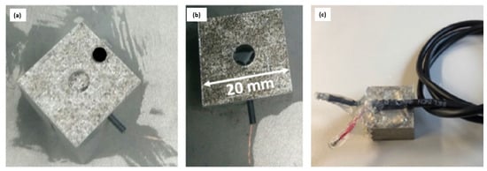 Figure 910. Procedure for integrating EC sensors: (a) removal of powder, placing heat-shrink tubes within protect wires, and passing wires through tubes; (b) cavity incorporation of the EC sensor; (c) specimens for the LPBF with soldered cables [78].
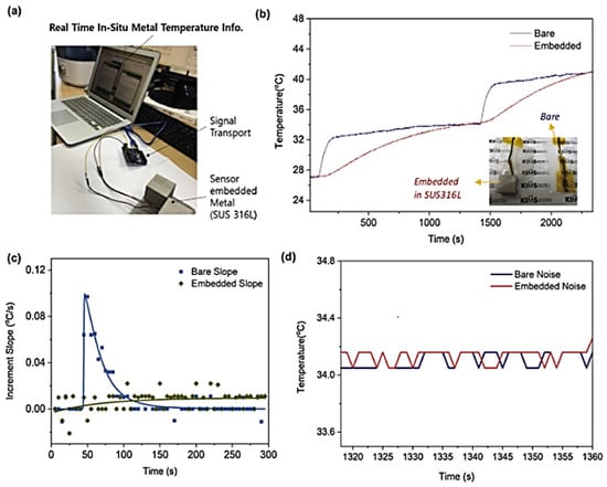 Figure 110. Temperature sensor operation processed by SE-SLM is validated by comparing data with a bare temperature sensor: (a) monitoring the in situ temperature of SE-SLM SUS316L using data reading configuration; (b) comparison of temperatures; (c) curve of temperature increase slope; (d) comparison of noise levels [81].
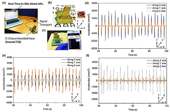 Figure 112. IC component based on PCB embedded in metal: (a) configuration of an IC chip inserted in a metal component; (b) Inconel 718 turbine vane integrated into an IC chip; (c) turbine vane temperature monitored wirelessly; acceleration data recorded for every vibration input axis (d) X-axis, (e) Y-axis, (f) Z-axis [81].
- (vi)
-
Inkjet-based embedded sensors
- (vii)
-
Hybrid additive manufacturing technologyTable 2.Summary of AM-based 3D printing methods and materials.
Printing Technology AM Based 3D Printing Methods Materials Performance of Materials References Extrusion-based printing Fused deposition modeling (FDM) Thermoplastics e.g., PLA, ABS, nylon The filament was melted and extruded through a high-temperature nozzle that was used for 3D translation. [13] 3D Inkjet Ultraviolet (UV) curable and low viscous materials Viscosity is crucial in 3D printing. It affects the quality of the printed object and speed of the printing process. Low viscosity materials require lower extrusion temperatures and fast printing speeds. [109][110][109,110] Direct ink writing (DIW) Elastomers, thermosets, metals, and ceramics in micro/nano particle solutions and biomaterials It can print materials at room temperature and in an ambient environment. Inks were formulated to exhibit shear-thinning and yield rheological behaviors, which are desired to be extruded smoothly and also maintain their shapes after extrusion. [111][112][111,112] Liquid resin-based printing Stereolithography (SLA) Light (UV, LEDs, or laser) curable polymers To create a solid layer, a UV laser is used to locally cure the resin along the printing routes or projected patterns. SLA uses a point-source laser light beam, but DLP increases printing speed by projecting pictures across the entire platform at each layer. [113][114][113,114] Direct light processing (DLP) [115] Powder-based printing Selective laser sintering (SLS) Metal and alloys, polymers, and semiconductors The particles are locally melted and fused together using a high-energy laser beam to create 3D geometry layer by layer. The platform is lowered after each layer is created, and fresh powder is added to print the subsequent layer. [116] Direct energy deposition (DED) For melting wire-based or powder-based filler materials, a high-energy beam is employed. It can be utilized in tandem with other subtractive manufacturing techniques and for repair reasons. [117] Laser powder bed fusion (LPBF) In it, a laser is used to melt and fuse powder. [114]

