1. Introduction
Si-based devices are widely used in power converters, which include bipolar, unipolar, controlled, and uncontrolled devices. Examples of such devices are power diodes, thyristors (gate turn-offs (GTO); gate-controlled thyristors (GCT)), BJTs (bipolar junction transistors), IGBTs, and MOSFETs. A new generation of IGBTs is now able to handle voltages up to 6.5 kV and currents up to 1700 A. The IGBT (insulated gate bipolar transistor) represents a power semiconductor device comprising four layers and three terminals. It serves as a merged unit combining the attributes of power MOSFET and BJT, facilitating rapid switching and elevated power-handling capacity. The IGBT is characterized by its capability to deliver efficient switching with minimal power loss in the ON state, along with superior ratings when compared to both MOSFET and BJT devices. IGBTs are commonly used in motor drives, converters circuits, and power supplies applications where there is a demand for high voltage and currents. Power MOSFETs, on the other hand, are increasingly used by the power supply community and in low-power inverters due to their high switching ability and ease of drive circuitry in contrast to IGBTs
[1]. Si-based MOSFETs have long been hindered due to their high on-state resistance, which substantially increases power losses in the devices. The on-state resistance increases in proportion with the blocking voltage, which makes them unsuitable for high-voltages applications above 600 V
[2].
The physical limitations of the current generation of Si-based MOSFETs and IGBTs have hindered the progress in achieving high efficiency, reliability, and compact form factor in power applications. It is desirable to convert power at high frequencies for power converters and other electronic system applications. There are many advantages when switching at higher frequencies, such as a reduction in the size, weight, and cost of the converter. The limitation of Si-based power semiconductors arises due to a decrease in efficiency and a substantial increase in temperature stress cycles as the switching frequency increases
[3].
In the last decade, numerous improvements have been made to the existing silicon technology in terms of structure, design, and material properties. As the demand for higher current, voltage, packaging density, and temperature is constantly growing, Si-based power devices have gradually started approaching their performance limits. While, WBG semiconductors have begun to emerge as a potential alternative technology. They offer better inherent material advantages over Si, such as higher voltage breakdown, higher switching frequency, comparable carrier mobility, higher energy bandgap, and higher thermal conductivity
[4].
WBG-based semiconductors such as silicon carbide (SiC), gallium nitride (GaN), and diamond (Dia) are superior to Si semiconductors and offer many advantages for power conversion applications. The physical characteristics of SiC, GaN, and Dia, include higher bandgap width (3~4 times), higher breakdown field (4–20 times), higher thermal conductivity (3–13 times), larger saturated electron drift velocity, low intrinsic carrier concentration (between 10–35 order of magnitude), and higher bandgap energy as compared to those of Si
[1].
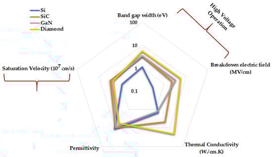
Figure 1 illustrates the thermal, voltage, and frequency characteristics of Si, SiC, and GaN materials.
Figure 1. Si, SiC, and GaN properties.
Other advantages of WBG semiconductors are their thinner drift regions due to increased electric critical field value, which can result in lower on-resistance and better coefficient of thermal expansion (CTE). Materials having CTE closer to the available electrically insulating and thermally conductive ceramics layers can be adopted more easily for higher power and temperature applications compared to Si. There are also some disadvantages of WBG semiconductors, such as their electrons and holes mobility, which might in some cases make them inappropriate for bipolar devices. For high-power and high-temperature applications, WBG semiconductors offer physical properties relatively superior to those of Si-based semiconductor technology. As temperature increases, the degradation of the semiconductor material will continue until it fails to provide sufficient functionality. There are certain amount of thermal electron and hole carriers called intrinsic carriers. As temperature increases, the number of carriers increases exponentially, which causes a degradation in the electrical conductivity of the doped regions in Si-based semiconductors. The other source of degradation is due to the P–N junction leakage current, which is directly related to the intrinsic concentration of the semiconductor. Since WBG semiconductors have lower intrinsic carrier concentration, the leakage currents are smaller as compared to silicon. Another fundamental mechanism in semiconductors is the ability of carriers to move through the semiconductor. When the temperature increases, the ability of carriers to move inside the crystal decreases. This is due to atoms in the crystal lattice acquiring more energy as the temperature increases, hence increasing the thermal vibrational energy that results in more collisions through the crystal. This leads to a reduction in the amount of current that a diode or a transistor can carry due to a decrease in carrier mobility
[5]. With the combination of improved material properties, WBG can significantly reduce losses by 95% up to 98% or higher depending on the application
[6]. This substantially reduces the cooling requirements and size of passive components, leading to a reduction in size, weight, and cost
[7].
Despite all these advantages, SiC-, GaN-, and Dia-based semiconductors are still in their early stages of research and development. Because of its higher thermal conductivity, ultrawide bandgap, and higher carrier mobility as compared to other semiconductors, Dia is set to become the best semiconductor material in the future. Even though Dia is the best semiconductor, the device material and fabrication technology is less mature and less developed as compared to SiC and GaN
[8]. Currently, the WBG semiconductors market represents a small segment in the global power electronics industry, and power electronics in turn are small fraction of the global semiconductor market. The U.S. is leading the market share for WBG research and development, but the rising competition from Europe, China, and Japan is changing this landscape
[9].
2. Performance Advances and Market Trends of SiC
There are many challenges that arise when developing new generation of WBG-based semiconductors for various applications. For SiC-based devices, the difficulty arises from the presence of crystal defects and lack of abundant wafers during the material processing. These factors have ultimately contributed to the slow commercial development of SiC power devices. SiC has well over 150 different polytypes, but only 6H-SiC and 4H-SiC are commercially available in the form of abundant wafers and epitaxial layers
[10]. Among these two, 4H-SiC exhibits better characteristics because of its higher carrier mobility and higher electric breakdown field, which helps reduce the size of the epitaxial layers. The reduction in the size of the drift layer helps reduce the low drift resistance, which in turn reduces the forward voltage drop and conduction losses
[11].
Table 1 presents a comparison between material properties of Si, 6H-SiC, and 4H-SiC semiconductors
[11].
Table 1. 4H-SiC, 6H-SiC, Si, and diamond material properties
[11].
SiC-based semiconductors are relatively new in the power industry. The first commercial power device was introduced in 2001 as the SiC-based Schottky diode
[12]. Despite being relatively new in the commercial marketplace, significant improvements have been made over the years. One of the SiC leading manufacturers, Cree, was the first to announce in 2012 the production of 150 mm SiC wafers and a range of power MOSFETs
[13]. Initially, SiC wafers suffered from defects such as micropipes; however, wafer quality has improved quite significantly over these past years. The defects were in the range of 5–10/cm
2 in 2006
[14], improving to 0.75/cm
2 in 2014
[15], and recently, the Japanese manufacturer Showa Denko lowered the defect densities of 150 mm (6 inch) SiC wafers by up to 0.25/cm
2 [16]. SiC devices’ cost is expected to decrease gradually as manufacturers improve the fabrication processes by improving the production capabilities and wafer sizes.
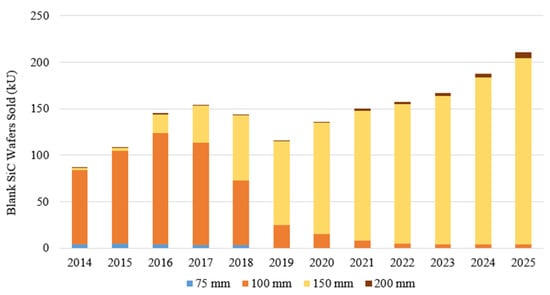
Figure 2 illustrates the current and future market demand for the 150 mm SiC wafer size in comparison to 100 mm
[17], while
Figure 3 depicts the key milestones in the research and development in SiC technology. Due to the improvements in wafer fabrication and increased production volumes, SiC power devices’ costs have significantly declined since the introduction of first SiC Schottky diode and MOSFETs. The initial cost of the SiC Schottky diode was USD 5000 for a two-inch wafer, USD 1200–USD 1400 in 2009 for a four-inch wafer, and USD 600–USD 750 in 2012
[18]. Also, during this time span, SiC power devices sales increased by three times over the years
[19].
Figure 2. Production of various SiC substrate wafers.
Figure 3. Milestones in SiC power electronics development.
Cree is one of the world’s largest growing power semiconductor manufacturers.
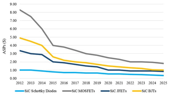
Figure 4 shows the Cree SiC power devices’ costs trend over the past few years
[20]. The performance of SiC power devices has also gradually improved over the last years since their introduction in 2001.
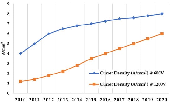
Figure 5 illustrates the current density growth from 2010 to 2012 and a prediction of future trends up to 2020
[21]. For high-voltage SiC power devices, there is a steady increase in current density, while for lower-voltage SiC power devices, the current density is expected to slow down around the end of this decade due to the cost of SiC modules and long-term reliability
[22]. In 2005, Schottky diodes were available at current rating up to 25 A; nowadays, the current ratings of these devices can reach 50 A
[23]. Also, significant progress has been made in SiC power MOSFETs technology, which led to an increase in the performance of each generation of devices. Due to SiC maturity over GaN, higher breakdown voltage and current capabilities are commercially available (SiC MOSFETs available up to 1.7 kV and thyristor up to 6.5 kV), while Wolfspeed (Cree) successfully tested 10 kV MOSFETs and further developed 15 kV SiC
[24]. In 2011, a 1200 V SiC MOSFET had switching losses around 0.78 mJ, and in 2013, the average switching losses of the next-generation SiC power MOSFETs were 0.56 mJ, i.e., a 28% decrease
[18]. These performance enhancements were the results of the recent advances made in material development and fabrication processes
[25].
Figure 4. Decline of device cost for Cree SiC products over the last years
[20].
Figure 5. Current density evolution for SiC
[26].
At present, SiC power electronics’ technological development and production is mainly carried out by a few key companies in the market.
Table 2 gives a list of these companies, their market share, and their revenue in 2010
[19]. In 2021, the global SiC power electronics industry was estimated to be worth USD 1.090 million and is due to reach USD 6.297 million by 2027
[27]. The companies leading the research and development are mainly Infineon, Mitsubishi Electric, ON Semiconductor, and STMicroelectronics. SiC fabrication facilities are mainly in Europe (55%), the United States (41%), and Japan (2%). By 2020, the market share of SiC devices is expected to shift radically, with Japan capturing 35% of the global market share due to considerable investment from the Japanese government and industry
[28]. Toyota is one of the Japanese car manufacturers currently testing hybrid vehicles and buses based on SiC power devices
[29].
Table 2. Distribution of leading SiC power electronics device makers by market share in 2021.
3. Performance Advances in GaN
GaN offers many features such as faster switching speed, smaller size, higher efficiency, and lower cost. Currently, GaN-based devices are already commercialized for lasers and RF applications, while for high-power applications, GaN technology is still at its early stage. Due to the lack of abundance of high-quality, defect-free GaN substrates, GaN epilayers are designed on foreign substrates such as Si, SiC, and sapphire. Among these, GaN epilayers grown on Si offer lower cost and better performance in comparison to the other substrate materials. AlGaN/GaN heterostructure field-effect transistors (HFETs) and high electron mobility transistor (HEMTs) have been commercially available since 2005 and have mostly been used in RF and optoelectronics. Recently, many power electronic design companies have opted for AlGaN/GaN HEMTs in various power applications, such as power converters. The most interesting property is the existence of two-dimensional electron gas (2DEG) formed in AlGaN/GaN structures due to the discontinuity difference between GaN and AlGaN. 2DEG is a gas of electrons free to move in two dimensions but tightly confined in the third. This tight confinement leads to quantized energy levels for motion in the third direction. Also, due to presence of polarization fields for AlGaN/GaN HEMTs, this allows for a high 2DEG concentration with large mobility values.
Table 3 shows GaN epilayers grown on different substrates and their properties
[30].
Table 3. GaN epilayers grown on different substrate properties
[30].
The developed power GaN HEMTs are increasingly entering the market and are well suited for high-power and high-voltage applications. This market is projected to achieve a significant performance improvement up to 100 times in comparison to Si
[31]. GaN HEMTs for normally on and normally off architectures are commercially available in the voltage breakdown range of 200 to 650 V. GaN-based MOSFETs are still undergoing research and development, and different manufacturers have developed and commercialized SiO
2/GaN-interfaced MOSFETs and AlGaN/GaN-based MOS-HEMTs with high blocking voltage (2.5 kV) and high channel mobility values (170 cm
2/Vs). In 2010, International Rectifier announced their first GaN on silicon HEMT for high-power applications. This release was quickly followed by the launch of GaN devices in the range of 200 V by Efficient Power Conversion (EPC). The success of these devices was due to improvements in GaN-on-silicon epitaxy techniques
[32]. This technique facilitated the creation of substrates with less impressive properties but at relatively low prices compared to GaN on SiC or GaN substrates. The price of the 4-inch silicon wafer was USD 100 for GaN epitaxy, while the 4-inch SiC wafer was at USD 130 and USD 7500 for the GaN wafer
[33].
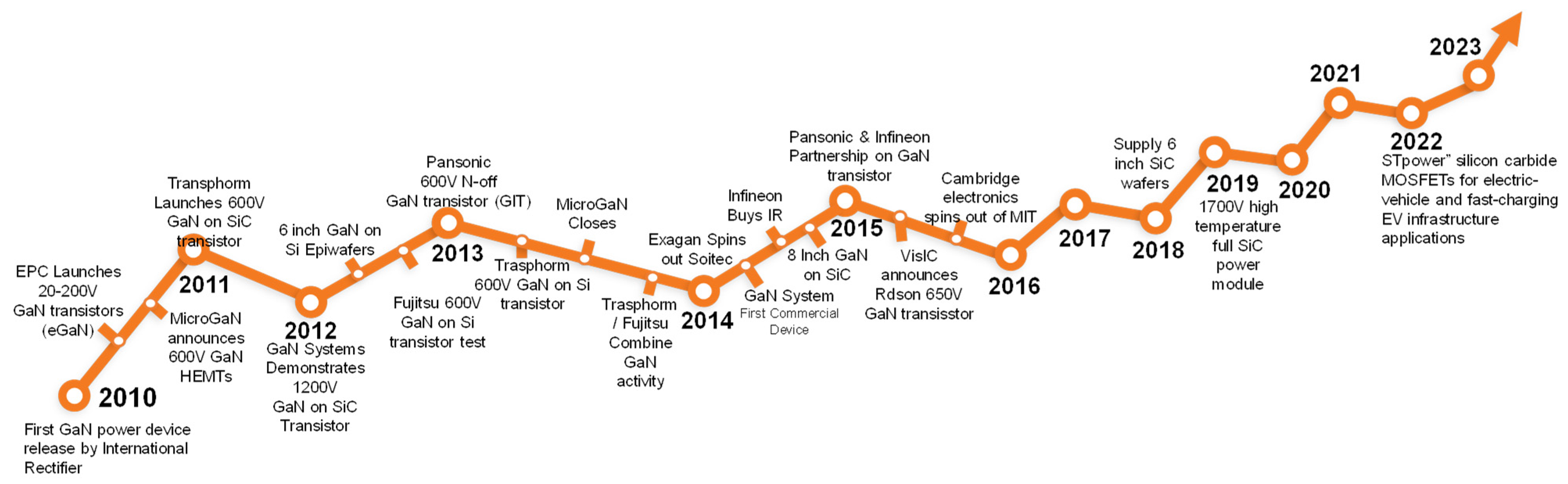
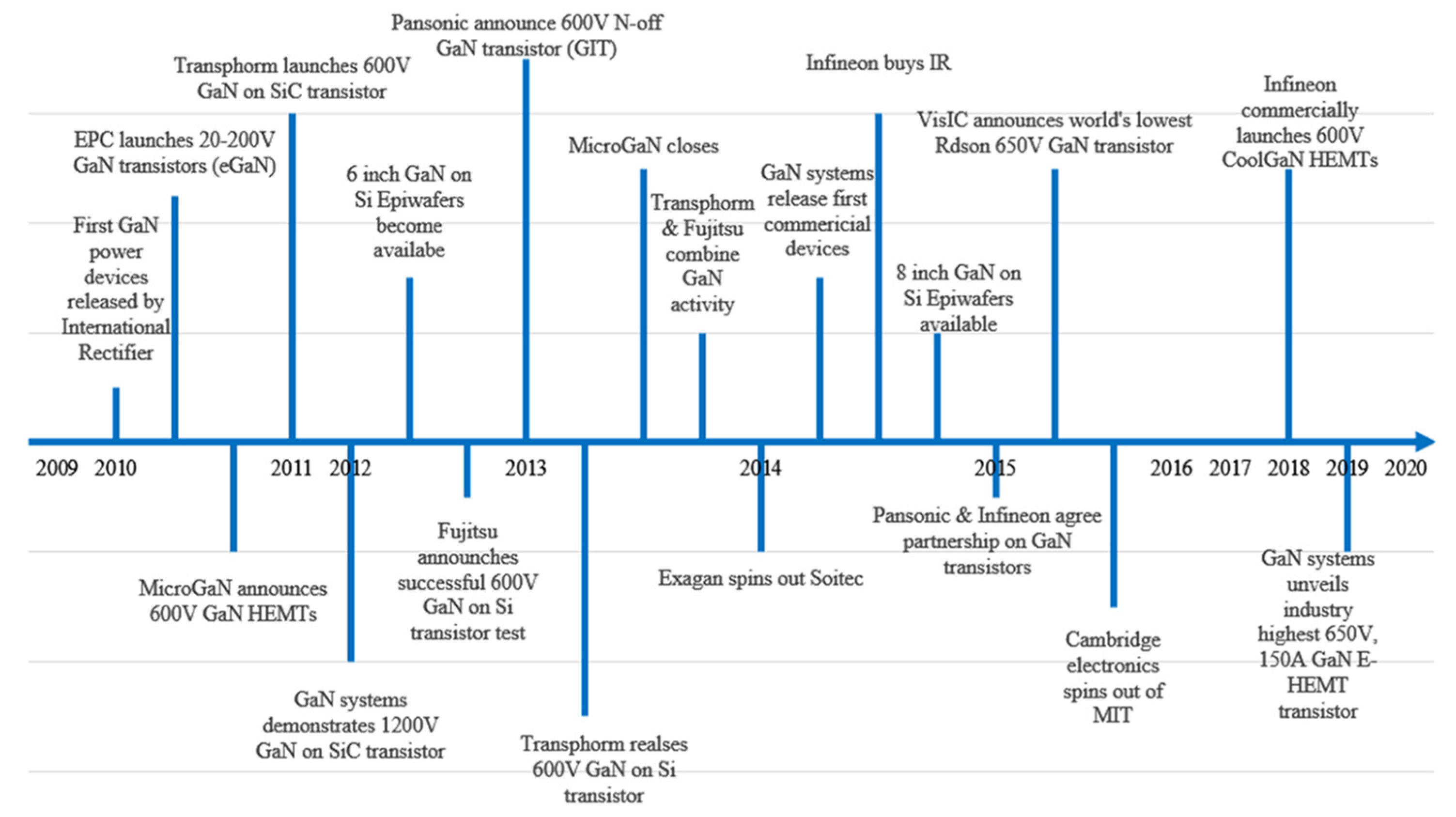
Figure 6 depicts the milestones and development of GaN power electronics devices throughout the past few years. The first GaN power devices were introduced during early 2010 to late 2011, where the first GaN power devices were released by International Rectifier, and since then, several successfully developed transistors have been reported, such as the GaN transistors (eGaN), 600 V GaN HEMTs, and 600 V GaN-on-SiC transistor. From early 2012 to mid-2014, the 6-inch GaN on Si was developed, whereas the 8-inch GaN on SiC was developed from mid-2014 to late 2016. Moreover, from 2018 to late 2019, the GaN system reached 150 A at 650 V
[34].
Figure 6. Milestones in GaN power electronics development.
The performance of GaN power devices has also improved since their introduction in 2010. Other GaN advancements include moving to larger 8-inch GaN-on-silicon wafers
[35] and the introduction of gate injection transistors (GITs) in the power electronics market. GITs are tailor-made to perform well in the high-voltage range, with some of the devices rated up to 600 V. The major progress in GaN devices’ research and development is attributed entirely to research labs and universities. The University of California Santa Barbara has been the leader in the development of high-quality GaN devices for power electronics
[35].
Most companies involved in GaN devices are from the U.S. apart from MicroGaN and Infineon Technologies. Initially, Efficient Power Conversion (EPC), Transphorm, and MicroGaN were solely involved in the development of GaN power electronics devices. Now, other major companies such as Panasonic, Infineon, and Texas Instruments, who have been traditionally involved with Si-based devices, are also developing GaN devices. GaN power market was worth USD 126 million in 2021 and is expected to reach USD 6 billion by 2027
[36].
4. Performance Advances in Diamond
Diamond’s outstanding physical and electrical characteristics, which includes the highest known thermal conductivity, excellent electrical insulator properties, high breakdown voltage, and high carrier mobility, make it theoretically the best semiconductor for the next generation of power electronic devices
[37]. Some of the potential applications include high-voltage power electronics, high-frequency high-power devices, and high-power optoelectronics devices, such as laser diodes and LEDs. During the last few years, diamond growth techniques have been significantly enhanced, and doping control methods for p, p+, n-type, and intrinsic diamond have been designed. Therefore, the electrical properties of diamond devices can now be characterized not just theoretically but also experimentally through device structures. Recently, planar diamond power Schottky barrier diode (SBD) test results reported a maximum breakdown field of 9.5 MV/m
[38], blocking voltage of Vmax > 10 kV
[39][40], high current operation above 20 A
[41], and low switching losses with fast operation
[42], making diamond SBDs an attractive material for power electronics applications. The first diamond-based power switching device was introduced in 1980s by Prins, using natural diamond crystals to form a bipolar junction transistor (BJT) with the usage of diamond crystals as the base electrode, while the n-type emitter and collector region were formed by carbon ion implantation
[43]. However, due to device’s geometrical issues associated with the fabrication process, the current gain was less than unity. Since then, other diamond-based power semiconductor devices such as metal-semiconductor FETs (MISFETs)
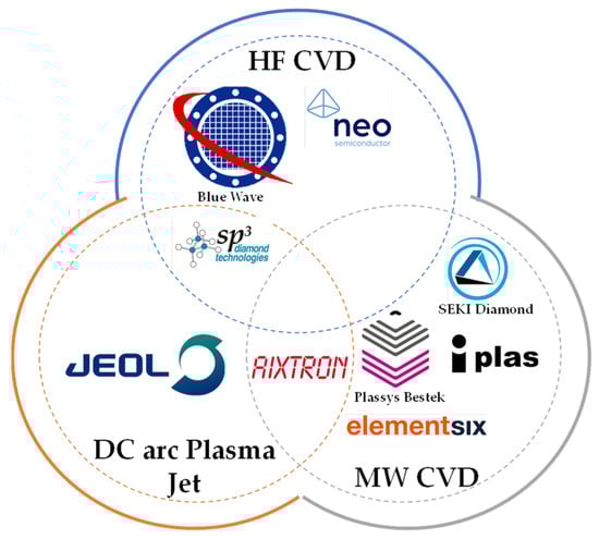
[44] and metal-insulator-semiconductor FETs (MISFETs) were also designed using diamond crystals through ion implantation or diffusion doping. In the last decade, the situation has drastically changed with the introduction of various techniques of diamond epitaxial growth by chemical vapor deposition (CVD), high-pressure high-temperature (HPHT), microwave-enhanced chemical vapor deposition (MWCVD), and mosaic-type method. Producing high-quality defect-free wafers produced from diamond crystals is still a big challenge even with the application of different single-crystal growth techniques. With the HPHT technique, high-quality defect-free wafers of only few millimeters have been achieved so far, while for the SiC wafer. sizes up to 150 mm are available. The MWCVD and mosaic-type techniques are quite promising and are approaching wafer sizes of 2 inches, even though the defect density needs to be reduced in order to commercialize the device on a large scale. Another interesting technique involves the heteroepitaxy of diamond on iridium, enabling the development of diamond films of up to 4 inches. Further development is required to reproduce controlled processes for manufacturing using this technique. Additionally, single-wafer material manufacturing for electronic applications is significantly impacted due to the difficulty of n-type doping with the lack of an efficient charge donor. Since p-type doping of naturally insulating diamond can easily be achieved by using boron, a great deal of development is being achieved on the fabrication of unipolar devices. Some of the CVD equipment makers for developing high-quality diamond wafers are shown in
Figure 7 [45]. They can be broadly categorized into two groups based on method: hot filament chemical vapor deposition (HF CVD) and MW CVD.
Figure 7. CVD equipment makers for development of high-quality diamond wafers.
5. Figure of Merit (FOM)
Various researchers have used numerous figures of merit (FOM) in order to evaluate different semiconductor materials performance. In 1965, Johnson
[46] evaluated WBG semiconductor material for the first time and proposed an equation that could help identify possible future semiconductor materials. This author proposed that a semiconductor transistor performance can be evaluated using the critical breakdown field
𝐸𝑐 and the electron drift velocity
VsatVsat and came up with a FOM as
JM=(𝐸𝑐Vsat/π)2. Later, Keyes
[27] defined another FOM to evaluate semiconductors device performance as
, where
λ is the thermal conductivity, and
𝜀 is the dielectric constant. In this FOM, power frequency for low-voltage transistors is also taken into account. When comparing these two FOMs, it becomes clear that saturation velocity and dielectric constant can be used on a broader level to evaluate some of the semiconductor devices. It is challenging, when evaluating a device’s performance completely, to consider simultaneously the material’s bandgap, thermal conductivity, and critical breakdown field.
To improve the efficiency and performance of semiconductor devices, it is essential to minimize power losses. Baliga
[47] proposed the FOM,
BM=𝜀𝜇𝐸3𝑐, where
𝜇 represents the carrier mobility. This FOM helps reduce the conduction losses in power FETs. This FOM can only be evaluated for low frequencies, as it assumes that power losses are only due to current flowing through the on-resistance. To include higher-frequency switching losses, the author proposed another FOM,
BHFM=𝜇𝐸2𝑐, which assumes that losses occur when charging and discharging the input capacitance of FETs
[48]. Another important factor contributing to power losses is the thermal conductivity. Shenai et al. defined three different thermal FOMs to incorporate various scenarios and factors. The first case scenario considers that if the thermal conductivity properties of heat sink material are different compared to active device area, then the FOM is defined as
QF1=λ𝜎A. In the case of perfect heat sink material and with the assumption of an active device area at ambient temperature, the FOM can be defined as
QF2=λ𝜎A𝐸𝑐. Finally, excluding any assumption related to heat sink material or geometry, the FOM can be defined as
QF3=𝜎. For all three cases,
𝜎A is equal to Baliga’s FOM (i.e.,
𝜀𝜇𝐸3𝑐)
[49].
As more accurate data relating to new semiconductor materials properties became available, FOMs slowly evolved over time. Chow
[50] discussed the problem with the assumption of the universal relationship between energy bandgap and breakdown voltage value when using Baliga’s FOM for low frequencies. This universal relationship is not true for WBG semiconductors and hence cannot be effectively used to evaluate some devices. Baliga’s FOM for higher frequencies is based on the assumption of linear relationship between energy bandgap and critical electric field, which is not true as well. Hence, there is a need for further investigation to develop new FOMs.
 +1 credit