 +1 credit
| Version | Summary | Created by | Modification | Content Size | Created at | Operation |
|---|---|---|---|---|---|---|
| 1 | Muhammad Ali Butt | -- | 1687 | 2023-08-22 10:56:12 | | | |
| 2 | Peter Tang | + 1 word(s) | 1688 | 2023-08-22 11:09:10 | | |
Video Upload Options
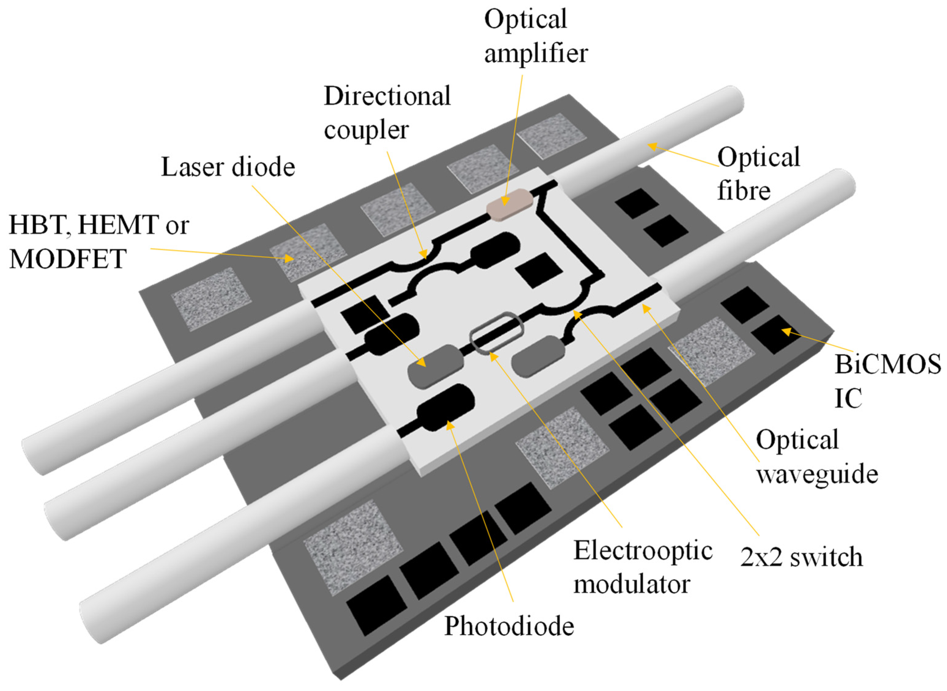
Silicon (Si) photonics is a groundbreaking technology that merges the fields of Si microelectronics and photonics to enable the manipulation and transmission of light on a Si chip. It leverages the exceptional properties of Si, such as its high refractive index and compatibility with existing electronic manufacturing processes, to create compact and highly efficient optical devices. Silicon photonics has been an area of active research and development. Researchers have been working on enhancing the integration density and intricacy of silicon photonic circuits. This involves the development of advanced fabrication techniques and novel designs to enable more functionalities on a single chip, leading to higher performance and more efficient systems.
1. Introduction
2. History
3. CMOS Fabrication
4. Recent Advances in Si Photonics for Telecommunication
|
Modulation Principle |
Structure |
Ebit (fJ/bit) |
ER (dB) |
References |
|---|---|---|---|---|
|
Electro-refractive |
MZI |
13.21 |
20.36 |
[54] |
|
Electro-optic |
MZI |
30.18 |
- |
[55] |
|
Electro-optic |
MZI |
- |
30 |
[56] |
|
Electro-optic |
MZI |
30 |
- |
[57] |
|
Carrier-depletion |
Ring |
- |
3.9 |
[58] |
|
Carrier-depletion |
Ring |
50 |
6.5 |
[59] |
|
Carrier-injection |
Ring |
120 |
7 |
[60] |
|
Carrier-depletion |
Ring |
680 |
8 |
[61] |
|
Carrier-depletion |
Ring |
- |
>10 |
[62] |
5. Si Photonics Sensors
|
Sensor |
Configuration |
Gas |
Sensitivity (nm/RIU) |
Q-Factor |
LOD (RIU) |
Refs. |
|---|---|---|---|---|---|---|
|
MZI |
RR-MZI |
He, N2 |
1458 5500 (Suspended MZI) |
- |
8.5 × 10⁻⁵ |
[64] |
|
RR |
RIB-slotted RR |
CO2, CH4 |
20,600 |
- |
3.675 × 10⁻⁴ |
[65] |
|
RR |
Slotted MRR |
CH4, CO2 |
2308 |
- |
- |
[66] |
|
RR |
Slotted RR |
CO2 |
300 |
- |
- |
[67] |
|
RR |
Slotted MRR |
Acetylene |
490 |
5000 |
10−5 |
[68] |
|
SPP |
PSWG |
CO2 |
- |
- |
274.6 (Free-standing structure) 70.1 (Asymmetric structure) |
[69] |
|
PhC |
Cryptophane-E-infiltrated PhC microcavity |
CH4 |
363.8 |
12,923 |
- |
[70] |
|
PhC |
PhC cavity |
Tetrahydrofuran (THF) vapor |
194 |
2 × 10⁵ |
4 × 10⁻⁵ |
[71] |
|
PhC |
PhC air-slot cavity |
CO2, N2, He |
510 |
2.6 × 10⁴ |
1 × 10⁻⁵ |
[72] |
|
PhC |
Slot PhC microcavities |
N2, CO2, He |
421 |
>3.0 × 10⁴ |
1 × 10⁻⁵ |
[73] |
References
- Yamada, K.; Tsuchizawa, T.; Nishi, H.; Kou, R.; Hiraki, T.; Takeda, K.; Fukuda, H.; Ishikawa, Y.; Wada, K.; Yamamoto, T. High-performance silicon photonics technology for telecommunications applications. Sci. Technol. Adv. Mater. 2014, 15, 024603.
- Sato, K.I. Design and Performance of Large Port Count Optical Switches for Intra Data Centre Application. In Proceedings of the 2020 22nd International Conference on Transparent Optical Networks (ICTON), Bari, Italy, 19–23 July 2020; pp. 1–4.
- Roelkens, G.; Abassi, A.; Cardile, P.; Dave, U.; De Groote, A.; De Koninck, Y.; Dhoore, S.; Fu, X.; Gassenq, A.; Hattasan, N.; et al. III-V-on-Silicon Photonic Devices for Optical Communication and Sensing. Photonics 2015, 2, 969–1004.
- Kazanskiy, N.L.; Khonina, S.N.; Butt, M.A. Advancement in Silicon Integrated Photonics Technologies for Sensing Applications in Near-Infrared and Mid-Infrared Region: A Review. Photonics 2022, 9, 331.
- Sajan, S.C.; Singh, A.; Sharma, P.K.; Kumar, S. Silicon Photonics Biosensors for Cancer Cells Detection—A Review. IEEE Sens. J. 2023, 23, 3366–3377.
- Khonina, S.N.; Kazanskiy, N.L.; Butt, M.A. Spectral characteristics of broad band-rejection filter based on Bragg grating, one-dimensional photonic crystal, and subwavelength grating waveguide—IOPscience. Phys. Scr. 2021, 96, 055505. Available online: https://iopscience.iop.org/article/10.1088/1402-4896/abe6be (accessed on 18 July 2023).
- Butt, M.A.; Kazanskiy, N.L.; Khonina, S.N. Advances in Waveguide Bragg Grating Structures, Platforms, and Applications: An Up-to-Date Appraisal. Biosensors 2022, 12, 497.
- Butt, M.A.; Khonina, S.N.; Kazanskiy, N.L. A T-shaped 1 × 8 balanced optical power splitter based on 90° bend asymmetric vertical slot waveguides. Laser Phys. 2019, 29, 046207.
- Butt, M.A.; Khonina, S.N.; Kazanskiy, N.L. Ultrashort inverted tapered silicon ridge-to-slot waveguide coupler at 1.55 µm and 3.392 µm wavelength. Appl. Opt. 2020, 59, 7821–7828.
- Melchior, H. Integrated Photonics Research (1998). In Indium Phosphide Photonic Waveguide Devices and Their Fiber Pigtailing; Optica Publishing Group: British, CO, Canada, 1998; p. IMA2. Available online: https://opg.optica.org/abstract.cfm?uri=IPR-1998-IMA2 (accessed on 18 July 2023).
- Wang, J.; Santamato, A.; Jiang, P.; Bonneau, D.; Engin, E.; Silverstone, J.W.; Lermer, M.; Beetz, J.; Kamp, M.; Höfling, S.; et al. Gallium arsenide (GaAs) quantum photonic waveguide circuits. Opt. Commun. 2014, 327, 49–55.
- Al-Douri, Y. Optical Waveguide of Lithium Niobate Nanophotonics. In Integrated Nanophotonics; John Wiley & Sons, Ltd.: Hoboken, NJ, USA, 2023; pp. 277–312.
- Chen, Q.; Zhu, Y.; Wu, D.; Li, T.; Li, Z.; Lu, C.; Chiang, K.S.; Zhang, X. Electrically generated optical waveguide in a lithium-niobate thin film. Opt. Express 2020, 28, 29895–29903.
- Butt, M.A.; Solé, R.; Pujol, M.C.; Ródenas, A.; Lifante, G.; Choudhary, A.; Murugan, G.S.; Shepherd, D.P.; Wilkinson, J.S.; Aguiló, M.; et al. Fabrication of Y-Splitters and Mach–Zehnder Structures on (Yb,Nb):RbTiOPO4/RbTiOPO4 Epitaxial Layers by Reactive Ion Etching. J. Light. Technol. 2015, 33, 1863–1871.
- Butt, M.A.; Nguyen, H.D.; Ródenas, A.; Romero, C.; Moreno, P.; de Aldana, J.R.V.; Aguiló, M.; Solé, R.M.; Pujol, M.C.; Díaz, F. Low-repetition rate femtosecond laser writing of optical waveguides in KTP crystals: Analysis of anisotropic refractive index changes. Opt. Express 2015, 23, 15343–15355.
- Butt, M.A. Integrated Optics: Platforms and Fabrication Methods. Encyclopedia 2023, 3, 824–838.
- Miller, S.E. Integrated optics: An introduction. Bell Syst. Tech. J. 1969, 48, 2059–2069.
- Gehler, J.; Bräuer, A.; Karthe, W.; Jäger, M. Antiresonant reflecting optical waveguides in strip configuration. Appl. Phys. Lett. 1994, 64, 276–278.
- Aarnio, J.; Heimala, P.; Del Giudice, M.; Bruno, F. Birefringence control and dispersion characteristics of silicon oxynitride optical waveguides. Electron. Lett. 1991, 25, 2317–2318.
- Zurhelle, D.; Schmidt, J.P.; Hoffmann, R.; Sander, D.; Mueller, J. Coupling structures for active and passive integrated optoelectronic components and circuits on silicon. In Proceedings of the Optoelectronic Integrated Circuit Materials, Physics, and Devices, San Jose, CA, USA, 6–9 February 1995; SPIE: Bellingham, WA, USA, 1995; Volume 2397, pp. 666–677.
- Gleine, W.; Muller, J. Laser trimming of SiON components for integrated optics. J. Light. Technol. 1991, 9, 1626–1629.
- Müller, J.; Dahms, U.P.; Mahnke, M.; Wunderlich, S. Refractive index relaxation in PECVD-and LPCVD-SiON-waveguides on silicon substrates. In Proceedings of the Conference on Integrated Optics, Delft, The Netherlands, 3–6 April 1995; pp. 303–308.
- Wunderlich, S.; Schmidt, J.P.; Müller, J. Integration of SiON waveguides and photodiodes on silicon substrates. Appl. Opt. 1992, 31, 4186–4189.
- Tu, Y.K.; Chou, J.C.; Cheng, S.P. Single-mode SiON/SiO2/Si optical waveguides prepared by plasma-enhanced chemical vapor deposition. Fiber Integr. Opt. 1995, 14, 133–139.
- Henry, C.H.; Blonder, G.E.; Kazarinov, R.F. Glass waveguides on silicon for hybrid optical packaging. J. Light. Technol. 1989, 7, 1530–1539.
- Hickernell, F.S.; Seaton, C.T. Channelized optical waveguides on silicon. Integr. Packag. Optoelectron. Devices 1987, 703, 164–174.
- Nagata, T.; Tanaka, T.; Miyake, K.; Kurotaki, H.; Yokoyama, S.Y.S.; Koyanagi, M.K.M. Micron-size optical waveguide for optoelectronic integrated circuit. Jpn. J. Appl. Phys. 1994, 33, 822.
- Soref, R.A.; Schmidtchen, J.; Petermann, K. Large single-mode rib waveguides in GeSi-Si and Si-on-SiO/sub 2. IEEE J. Quantum Electron. 1991, 27, 1971–1974.
- Splett, A.O.; Schmidtchen, J.; Schueppert, B.; Petermann, K. Integrated optical channel waveguides in silicon using SiGe alloys. In Proceedings of the Physical Concepts of Materials for Novel Optoelectronic Device Applications II: Device Physics and Applications, Aachen, Germany, 28 October–2 November 1991; SPIE: Bellingham, WA, USA, 1991; Volume 1362, pp. 827–833.
- Namavar, F.; Soref, R.A. Optical waveguiding in Si/Si1− x Ge x/Si heterostructures. J. Appl. Phys. 1991, 70, 3370–3372.
- Weiss, B.L.; Yang, Z.; Namavar, F. Wavelength dependent propagation loss characteristics of SiGe/Si planar waveguides. Electron. Lett. 1992, 28, 2218–2220.
- Grant, M.F. Integrated optical waveguide devices on silicon for optical communications. In Proceedings of the IEE Colloquium on Planar Silicon Hybrid Optoelectronics (Digest No. 1994/198), London, UK, 24 October 1994; IET: Stevenage, UK, 1994; pp. 1/1–110.
- Najafi, S.I.; Honkanen, S.; Tervonen, A. Recent progress in glass integrated optical circuits. Integr. Opt. Microstruct. II 1994, 2291, 6–12.
- Habara, K.; Matsunaga, T. Silica glass waveguide planar lightwave circuit applications in photonic switching. In Proceedings of the Photonic Switching, Minsk, Belarus, 1–3 July 1992; SPIE: Bellingham, WA, USA, 1993; Volume 1807, pp. 418–421.
- Tang, X.; Wongchotigul, K.; Spencer, M.G. Optical waveguide formed by cubic silicon carbide on sapphire substrates. Appl. Phys. Lett. 1991, 58, 917–918.
- Jackson, S.M.; Reed, G.T.; Reeson, K.J. Wave-Guiding in epitaxial 3c-Silicon carbide on silicon. Electron. Lett. 1995, 31, 1438–1439.
- Liu, Y.M.; Prucnal, P.R. Low-loss silicon carbide optical waveguides for silicon-based optoelectronic devices. IEEE Photonics Technol. Lett. 1993, 5, 704–707.
- Iyer, S.S.; Xie, Y.-H. Light Emission from Silicon. Science 1993, 260, 40–46.
- Soref, R.A. Silicon-based optoelectronics. Proc. IEEE 1993, 81, 1687–1706.
- Huang, Y.; Zhao, Q.; Kamyab, L.; Rostami, A.; Capolino, F.; Boyraz, O. Sub-micron silicon nitride waveguide fabrication using conventional optical lithography. Opt. Express 2015, 23, 6780–6786.
- Okazaki, S. High resolution optical lithography or high throughput electron beam lithography: The technical struggle from the micro to the nano-fabrication evolution. Microelectron. Eng. 2015, 133, 23–35.
- Zheng, Y.; Gao, P.; Tang, X.; Liu, J.; Duan, J. Effects of electron beam lithography process parameters on structure of silicon optical waveguide based on SOI. J. Cent. South Univ. 2022, 29, 3335–3345.
- Broers, A.N.; Hoole, A.C.F.; Ryan, J.M. Electron beam lithography—Resolution limits. Microelectron. Eng. 1996, 32, 131–142.
- Bruinink, C.M.; Burresi, M.; de Boer, M.J.; Segerink, F.B.; Jansen, H.V.; Berenschot, E.; Reinhoudt, D.N.; Huskens, J.; Kuipers, L. Nanoimprint Lithography for Nanophotonics in Silicon. Nano Lett. 2008, 8, 2872–2877.
- Shneidman, A.V.; Becker, K.P.; Lukas, M.A.; Torgerson, N.; Wang, C.; Reshef, O.; Burek, M.J.; Paul, K.; McLellan, J.; Lončar, M. All-Polymer Integrated Optical Resonators by Roll-to-Roll Nanoimprint Lithography. ACS Photonics 2018, 5, 1839–1845.
- Hiscocks, M.P.; Ganesan, K.; Gibson, B.C.; Huntington, S.T.; Ladouceur, F.; Prawer, S. Diamond waveguides fabricated by reactive ion etching. Opt. Express 2008, 16, 19512–19519.
- Kim, T.; Lee, J. Optimization of deep reactive ion etching for microscale silicon hole arrays with high aspect ratio. Micro Nano Syst. Lett. 2022, 10, 12.
- Bauhuber, M.; Mikrievskij, A.; Lechner, A. Isotropic wet chemical etching of deep channels with optical surface quality in silicon with HNA based etching solutions. Mater. Sci. Semicond. Process. 2013, 16, 1428–1433.
- Butt, M.A.; Kozłowski, Ł.; Piramidowicz, R. Numerical scrutiny of a silica-titania-based reverse rib waveguide with vertical and rounded sidewalls. Appl. Opt. 2023, 62, 1296–1302.
- Li, W.; Luo, Y.; Xiong, B.; Sun, C.; Wang, L.; Wang, J.; Han, Y.; Yan, J.; Wei, T.; Lu, H. Fabrication of GaN-based ridge waveguides with very smooth and vertical sidewalls by combined plasma dry etching and wet chemical etching. Phys. Status Solidi A 2015, 212, 2341–2344.
- Butt, M.A.; Khonina, S.N.; Kazanskiy, N.L. 2D-Photonic crystal heterostructures for the realization of compact photonic devices. Photonics Nanostructures Fundam. Appl. 2021, 44, 100903.
- Butt, M.A.; Kazanskiy, N.L. Two-dimensional photonic crystal heterostructure for light steering and TM-polarization maintaining applications—IOPscience. Laser Phys. 2021, 31, 036201. Available online: https://iopscience.iop.org/article/10.1088/1555-6611/abd8ca (accessed on 18 July 2023).
- Quack, N.; Takabayashi, A.Y.; Sattari, H.; Edinger, P.; Jo, G.; Bleiker, S.J.; Errando-Herranz, C.; Gylfason, K.B.; Niklaus, F.; Khan, U.; et al. Integrated silicon photonic MEMS. Microsyst. Nanoeng. 2023, 9, 27.
- Ayoub, A.B.; Swillam, M.A. Optical modulator using ultra-thin silicon waveguide in SOI hybrid technology. Opt. Quantum Electron. 2022, 54, 181.
- Sato, H.; Miura, H.; Qiu, F.; Spring, A.M.; Kashino, T.; Kikuchi, T.; Ozawa, M.; Nawata, H.; Odoi, K.; Yokoyama, S. Low driving voltage Mach-Zehnder interference modulator constructed from an electro-optic polymer on ultra-thin silicon with a broadband operation. Opt. Express 2017, 25, 768–775.
- Kieninger, C.; Füllner, C.; Zwickel, H.; Kutuvantavida, Y.; Kemal, J.N.; Eschenbaum, C.; Elder, D.L.; Dalton, L.R.; Freude, W.; Randel, S. Silicon-organic hybrid (SOH) Mach-Zehnder modulators for 100 GBd PAM4 signaling with sub-1 dB phase-shifter loss. Opt. Express 2020, 28, 24693–24707.
- Wang, C.; Zhang, M.; Chen, X.; Bertrand, M.; Shams-Ansari, A.; Chandrasekhar, S.; Winzer, P.; Lončar, M. Integrated lithium niobate electro-optic modulators operating at CMOS-compatible voltages. Nature 2018, 562, 101–104.
- Hu, Y.; Xiao, X.; Xu, H.; Li, X.; Xiong, K.; Li, Z.; Chu, T.; Yu, Y.; Yu, J. High-speed silicon modulator based on cascaded microring resonators. Opt. Express 2012, 20, 15079–15085.
- Dong, P.; Liao, S.; Feng, D.; Liang, H.; Zheng, D.; Shafiiha, R.; Kung, C.-C.; Qian, W.; Li, G.; Zheng, X. Low V pp, ultralow-energy, compact, high-speed silicon electro-optic modulator. Opt. Express 2009, 17, 22484–22490.
- Chen, L.; Preston, K.; Manipatruni, S.; Lipson, M. Integrated GHz silicon photonic interconnect with micrometer-scale modulators and detectors. Opt. Express 2009, 17, 15248–15256.
- Li, J.; Li, G.; Zheng, X.; Raj, K.; Krishnamoorthy, A.V.; Buckwalter, J.F. A 25-Gb/s Monolithic Optical Transmitter with Micro-Ring Modulator in 130-nm SoI CMOS. IEEE Photonics Technol. Lett. 2013, 25, 1901–1903.
- Ziebell, M.; Marris-Morini, D.; Rasigade, G.; Crozat, P.; Fédéli, J.-M.; Grosse, P.; Cassan, E.; Vivien, L. Ten Gbit/s ring resonator silicon modulator based on interdigitated PN junctions. Opt. Express 2011, 19, 14690–14695.
- Conteduca, D.; Arruda, G.S.; Barth, I.; Wang, Y.; Krauss, T.F.; Martins, E.R. Beyond Q: The Importance of the Resonance Amplitude for Photonic Sensors. ACS Photonics 2022, 9, 1757–1763.
- Taha, A.M.; Yousuf, S.; Dahlem, M.S.; Viegas, J. Highly-Sensitive Unbalanced MZI Gas Sensor Assisted With a Temperature-Reference Ring Resonator. IEEE Photonics J. 2022, 14, 6657709.
- Troia, B.; Passaro, V.M.N. Investigation of a novel silicon-on-insulator Rib-Slot photonic sensor based on the vernier effect and operating at 3.8 µm. J. Eur. Opt. Soc. Rapid Publ. 2014, 9, 14005. Available online: http://www.jeos.org/index.php/jeos_rp/article/view/951 (accessed on 18 July 2023).
- Zhang, W.; Zhang, X.; Zhang, X.; Jin, H.; Jin, Q.; Jian, J. A single slot micro-ring structure for simultaneous CO2 and CH4 gas sensing. Eur. Phys. J. Appl. Phys. 2018, 82, 30502.
- Tomono, Y.; Hoshi, H.; Shimizu, H. CO2 Detection with Si Slot Waveguide Ring Resonators toward On-chip Specific Gas Sensing. In Proceedings of the Conference on Lasers and Electro-Optics, San Jose, CA, USA, 5–10 May 2019; Optica Publishing Group: San Jose, CA, USA, 2019; p. JTh2A.96.
- Robinson, J.T.; Chen, L.; Lipson, M. On-chip gas detection in silicon optical microcavities. Opt. Express 2008, 16, 4296–4301.
- Saeidi, P.; Jakoby, B.; Pühringer, G.; Tortschanoff, A.; Stocker, G.; Dubois, F.; Spettel, J.; Grille, T.; Jannesari, R. Designing Mid-Infrared Gold-Based Plasmonic Slot Waveguides for CO2-Sensing Applications. Sensors 2021, 21, 2669.
- Zhang, Y.; Zhao, Y.; Wang, Q. Measurement of methane concentration with cryptophane E infiltrated photonic crystal microcavity. Sens. Actuators B Chem. 2015, 209, 431–437.
- Wang, X.; Lv, J.; E, S.; Han, B.; Zhang, Y. Theoretical Design and Simulation Optimization of Photonic Crystal Cavity for Tetrahydrofuran Vapor Sensing. Phys. Status Solidi B 2019, 256, 1900221.
- Jágerská, J.; Zhang, H.; Diao, Z.; Thomas, N.L.; Houdré, R. Refractive index sensing with an air-slot photonic crystal nanocavity. Opt. Lett. 2010, 35, 2523–2525.
- Li, K.; Li, J.; Song, Y.; Fang, G.; Li, C.; Feng, Z.; Su, R.; Zeng, B.; Wang, X.; Jin, C. Ln Slot Photonic Crystal Microcavity for Refractive Index Gas Sensing. IEEE Photonics J. 2014, 6, 6802509.

