Silicon (Si) photonics is a groundbreaking technology that merges the fields of Si microelectronics and photonics to enable the manipulation and transmission of light on a Si chip. It leverages the exceptional properties of Si, such as its high refractive index and compatibility with existing electronic manufacturing processes, to create compact and highly efficient optical devices. Silicon photonics has been an area of active research and development. Researchers have been working on enhancing the integration density and intricacy of silicon photonic circuits. This involves the development of advanced fabrication techniques and novel designs to enable more functionalities on a single chip, leading to higher performance and more efficient systems.
1. Introduction
Silicon (Si) photonics is a groundbreaking technology that merges the fields of Si microelectronics and photonics to enable the manipulation and transmission of light on a Si chip. It leverages the exceptional properties of Si, such as its high refractive index and compatibility with existing electronic manufacturing processes, to create compact and highly efficient optical devices. Si photonics has the potential to revolutionize various domains, including telecommunications, data centers, sensing, and biomedical applications [
1,
2,
3,
4,
5], by offering high-speed data transmission, low power use, and integration with electronic systems. Its ability to seamlessly integrate photonics with Si electronics opens new avenues for the development of advanced, scalable, and cost-effective solutions for a wide range of applications.
Si, the second most abundant element on Earth after oxygen, possesses exceptional qualities that make it highly suitable for various applications. Its simple cubic crystal structure allows production of defect-free wafers with remarkable purity. Additionally, Si’s thermal conductivity, hardness, and low density are advantageous in semiconductor devices. At a specific wavelength, Si demonstrates a high refractive index and remains transparent to infrared light. The high refractive index of Si allows the miniaturization of devices to incredibly small scales. Moreover, the well-established techniques used in semiconductor processing can be easily applied to Si photonics, enabling cost-effective mass production. Another advantage of Si is its high-quality native oxide, which offers superior characteristics compared with other semiconductors. The oxide serves as an excellent material for Si waveguide (WG) cladding and can host rare-earth dopants for integrated circuits. By controlling the oxide cladding layer, it becomes possible to manipulate light propagation within Si WGs. These properties collectively position Si photonics as a promising solution for integrating photonic circuits.
Si photonics integrated circuits rely on key components to manipulate and control light signals. WGs guide light through total internal reflection, whereas modulators alter light intensity or phase. Photodetectors convert optical signals to electrical ones, and filters selectively transmit specific wavelengths [
6,
7]. Splitters and couplers distribute and combine signals, and optical amplifiers enhance weak signals. These building blocks enable applications in optical communication, data centers, sensing, and biomedical imaging, propelling advancements in photonics technology [
8].
Researchers have made substantial progress in increasing the sensitivity and limit of detection (LoD) of Si photonic sensors. By enhancing the design of WGs and resonators and incorporating advanced materials, these sensors can now detect even smaller quantities of substances, making them suitable for a wider range of applications, including environmental monitoring, healthcare, and security. The integration of sensors on a single Si chip offers numerous benefits, including reduced size, increased portability, and cost-effectiveness. The ability to combine multiple sensors on a single chip allows for compact and robust sensing platforms that can be easily mass-produced. Moreover, advancements in fabrication techniques, such as nanofabrication and complementary metal oxide semiconductor (CMOS)-compatible processes, have enabled the cost-effective mass production of Si photonic sensors [
9]. This scalability has opened new opportunities for commercial applications and broader adoption of the technology.
Although Si photonics offers numerous advantages, it is worth noting that other optical platforms, such as indium phosphide (InP) [
10], gallium arsenide (GaAs) [
11], lithium niobate (LiNbO
3) [
12,
13], and rubidium titanyl phosphate (RTP) [
14,
15], also have their own unique strengths and are preferred for certain specialized applications. The choice of platform depends on factors such as performance requirements, cost considerations, and the specific needs of the application at hand. For more detailed information on optical platforms and fabrication methods, we recommend readers to see [
16].
2. History
Since the 1970s, researchers have envisioned an optical super chip with integrated optical components [
20]. Early studies focused on ferroelectric materials such as lithium niobate (LiNbO
3) and III-V semiconductors such as gallium arsenide (GaAs) and indium phosphide (InP). LiNbO
3 stood out for its significant electrooptic coefficient, enabling optical modulation through the Pockels effect. Meanwhile, the III-V compounds offered advantages in terms of laser fabrication, optical amplification, and electronic integration. Si’s widespread use as the preferred semiconductor in electronics prompted researchers to explore the possibilities of Si photonic circuits. This was mainly driven by the potential benefits of integrating photonics and electronics cost effectively. Si has a high refractive index compared with other common materials used in photonics. This property allows for strong light confinement and efficient light guiding within Si WGs and resonators. Consequently, Si photonic components can be designed on a small scale due to the strong confinement of light within Si WGs. This compactness is especially advantageous for on-chip integration and the creation of complex optical circuits. The investigation of Si photonic circuits started in the mid-1980s and has been ongoing since then. A significant volume of research has been conducted on various materials such as SiON [
21,
22,
23,
24,
25,
26,
27], Si
3N
4 [
28,
29,
30], SiGe [
31,
32,
33,
34], SiO
2 [
35,
36,
37], and SiC [
38,
39,
40]. These materials have been explored concerning their compatibility with standard CMOS technology. Si dominates as the primary semiconductor material for electronics due to its affordability, well-understood properties, and optical confinement capabilities. However, its indirect bandgap limits its effectiveness as a light-emitting material. Researchers have thus sought ways to modify Si’s structure for light emission [
41].
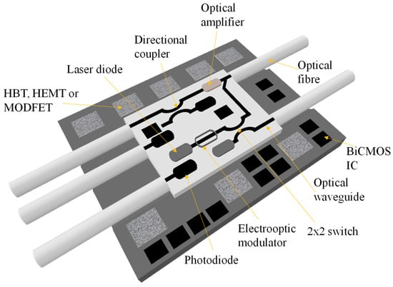
Additional efforts were undertaken to define a completely integrated monolithic optoelectronic super chip for Si hybrid integration. This idea was later modified to introduce a hybrid device that relied on a Si platform, incorporating Si optical WGs [
42] as depicted in
Figure 1.
Figure 1. Si-based super chip. Inspired by [
42].
3. CMOS Fabrication
CMOS is a semiconductor technology commonly used in electronic devices and integrated circuits and is crucial for Si photonics, enabling the integration of photonic and electronic elements on a single Si chip. CMOS technology is widely adopted for its energy efficiency, scalability, and versatility, making it a fundamental component in the design and manufacture of modern electronics [
16]. Photolithography, using optical or extreme ultraviolet (EUV) light, transfers patterns onto a Si wafer coated with photosensitive material. Ultraviolet lithography (UVL) represents a distinct form of photolithography wherein UV light serves as the exposure source [
43]. This technique finds extensive application in semiconductor manufacturing and various industries to produce patterns on a substrate. The utilization of UV light with its shorter wavelength enhances resolution and facilitates the creation of smaller, complex devices [
44]. Nonetheless, UVL demands meticulous attention and specialized equipment due to its distinctive properties. Electron beam lithography (EBL) is a potent nanofabrication technique that achieves extremely high-resolution patterns in nanometers, enabling precise nanostructures and devices [
45]. Though versatile, it is relatively slow and expensive compared with other lithography methods due to the time-consuming electron beam scanning process [
46]. Nanoimprint lithography (NIL) offers a cost-effective alternative [
47] to high-resolution lithography techniques such as EBL. It enables high-throughput production by processing large substrate areas simultaneously [
48]. Additionally, unlike EBL, NIL does not necessitate complex and expensive equipment.
Reactive ion etching (RIE) [
49,
50] and chemical wet etching [
51,
52] are common techniques in microfabrication and semiconductor manufacturing. They offer selective material removal from a substrate for pattern creation. Chemical wet etching suits simple and large-area patterning, whereas RIE is better for high-resolution and anisotropic etching [
53].
The combination of CMOS technology with various lithography and etching techniques enables the creation of complex and high-performance photonics devices that drive technological advancements in a wide range of industries. As technology continues to evolve, further innovations in CMOS and lithography techniques will likely contribute to even more exciting developments in the field of photonics and beyond.
4. Recent Advances in Si Photonics for Telecommunication
Recent progresses in Si photonics have greatly impacted the field of telecommunications. It combines the advantages of Si-based electronic circuits with the speed and bandwidth of optical communications, enabling the development of highly efficient and scalable optical devices [
54,
55]. By integrating optical components such as modulators, detectors, and WGs directly onto a Si chip, Si photonics allows for the seamless integration of optical and electronic functionalities. This technology enables high-speed data transmission over long distances, facilitates the growth of data-intensive applications, and provides a pathway for the development of compact, low-cost, and energy-efficient telecommunication systems. Its compatibility with existing Si manufacturing processes makes it an attractive solution for driving the next generation of communication networks, data centers, and high-performance computing infrastructures [
56].
In Table 1, a comprehensive analysis is provided, showcasing the performance of different Si-based modulators that feature diverse structures.
Table 1. Performance analysis of Si-based modulators employing MZI and ring structures.
|
Modulation Principle
|
Structure
|
Ebit (fJ/bit)
|
ER (dB)
|
References
|
|
Electro-refractive
|
MZI
|
13.21
|
20.36
|
[73]
|
|
Electro-optic
|
MZI
|
30.18
|
-
|
[71]
|
|
Electro-optic
|
MZI
|
-
|
30
|
[72]
|
|
Electro-optic
|
MZI
|
30
|
-
|
[70]
|
|
Carrier-depletion
|
Ring
|
-
|
3.9
|
[88]
|
|
Carrier-depletion
|
Ring
|
50
|
6.5
|
[87]
|
|
Carrier-injection
|
Ring
|
120
|
7
|
[79]
|
|
Carrier-depletion
|
Ring
|
680
|
8
|
[81]
|
|
Carrier-depletion
|
Ring
|
-
|
>10
|
[83]
|
5. Si Photonics Sensors
Si photonic sensors have gained significant attention and interest in both gas sensing and biosensing applications due to their exclusive advantages, such as high sensitivity, miniaturization capabilities, and potential for integration with existing Si-based electronic systems [
152].
A comprehensive comparison and summary of the performance of various optical gas sensors can be found in Table 2. By examining the data presented in Table 2, readers can gain insights into the strengths and limitations of each sensor type, aiding in the selection and implementation of appropriate optical gas sensing technologies for specific applications.
Table 2. Comparative overview of cutting-edge optical sensors designed for detecting different types of gases.
|
Sensor
|
Configuration
|
Gas
|
Sensitivity (nm/RIU)
|
Q-Factor
|
LOD (RIU)
|
Refs.
|
|
MZI
|
RR-MZI
|
He, N2
|
1458
5500
(Suspended MZI)
|
-
|
8.5 × 10⁻⁵
|
[204]
|
|
RR
|
RIB-slotted RR
|
CO2, CH4
|
20,600
|
-
|
3.675 × 10⁻⁴
|
[205]
|
|
RR
|
Slotted MRR
|
CH4, CO2
|
2308
|
-
|
-
|
[206]
|
|
RR
|
Slotted RR
|
CO2
|
300
|
-
|
-
|
[207]
|
|
RR
|
Slotted MRR
|
Acetylene
|
490
|
5000
|
10−5
|
[209]
|
|
SPP
|
PSWG
|
CO2
|
-
|
-
|
274.6
(Free-standing structure)
70.1
(Asymmetric structure)
|
[212]
|
|
PhC
|
Cryptophane-E-infiltrated PhC microcavity
|
CH4
|
363.8
|
12,923
|
-
|
[224]
|
|
PhC
|
PhC cavity
|
Tetrahydrofuran (THF) vapor
|
194
|
2 × 10⁵
|
4 × 10⁻⁵
|
[226]
|
|
PhC
|
PhC air-slot cavity
|
CO2, N2, He
|
510
|
2.6 × 10⁴
|
1 × 10⁻⁵
|
[227]
|
|
PhC
|
Slot PhC microcavities
|
N2, CO2, He
|
421
|
>3.0 × 10⁴
|
1 × 10⁻⁵
|
[228]
|
This entry is adapted from the peer-reviewed paper 10.3390/mi14081637