Submitted Successfully!
To reward your contribution, here is a gift for you: A free trial for our video production service.
Thank you for your contribution! You can also upload a video entry or images related to this topic.
Version Summary Created by Modification Content Size Created at Operation
1 -- 4837 2022-11-10 09:41:38 |
2 format correct Meta information modification 4837 2022-11-11 01:50:27 |

Video Upload Options

Do you have a full video?

Confirm

Are you sure to Delete?
Cite
If you have any further questions, please contact Encyclopedia Editorial Office.
Lu, D.;  Jiang, Q.;  Ma, X.;  Zhang, Q.;  Fu, X.;  Fan, L. Defect-Related Etch Pits on Crystals and Their Utilization. Encyclopedia. Available online: https://encyclopedia.pub/entry/33903 (accessed on 28 March 2024).
Lu D,  Jiang Q,  Ma X,  Zhang Q,  Fu X,  Fan L. Defect-Related Etch Pits on Crystals and Their Utilization. Encyclopedia. Available at: https://encyclopedia.pub/entry/33903. Accessed March 28, 2024.
Lu, Dongzhu, Quantong Jiang, Xiumin Ma, Qichao Zhang, Xiaole Fu, Liang Fan. "Defect-Related Etch Pits on Crystals and Their Utilization" Encyclopedia, https://encyclopedia.pub/entry/33903 (accessed March 28, 2024).
Lu, D.,  Jiang, Q.,  Ma, X.,  Zhang, Q.,  Fu, X., & Fan, L. (2022, November 10). Defect-Related Etch Pits on Crystals and Their Utilization. In Encyclopedia. https://encyclopedia.pub/entry/33903
Lu, Dongzhu, et al. "Defect-Related Etch Pits on Crystals and Their Utilization." Encyclopedia. Web. 10 November, 2022.
Defect-Related Etch Pits on Crystals and Their Utilization
Edit

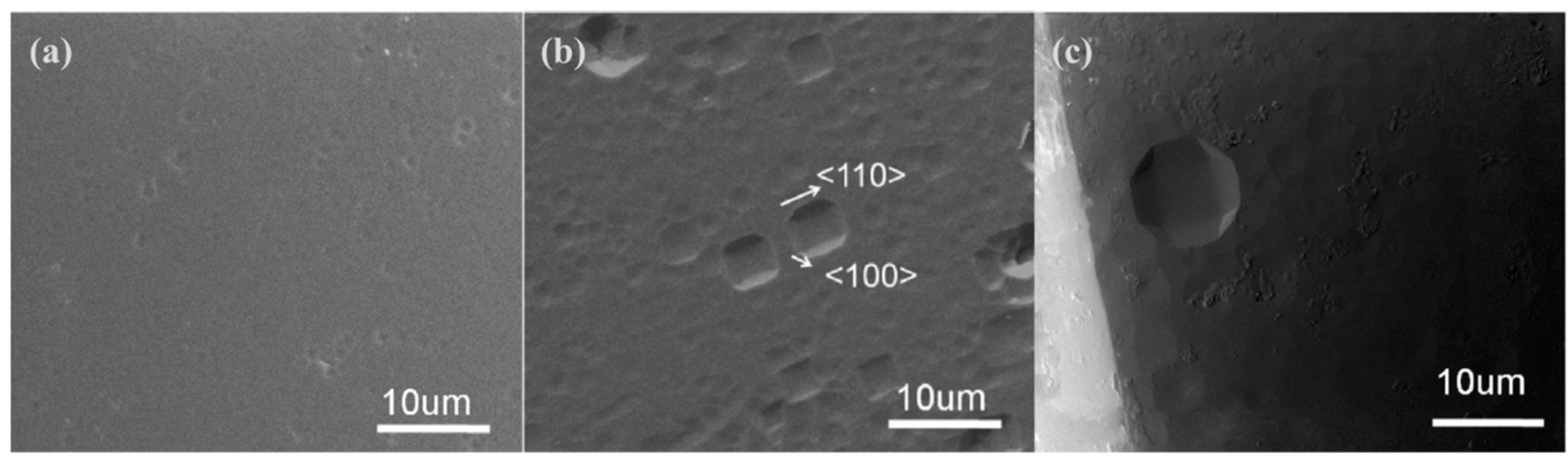
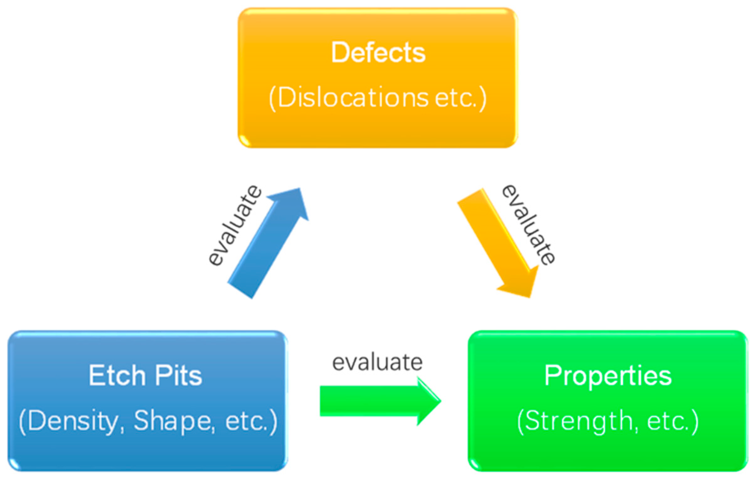
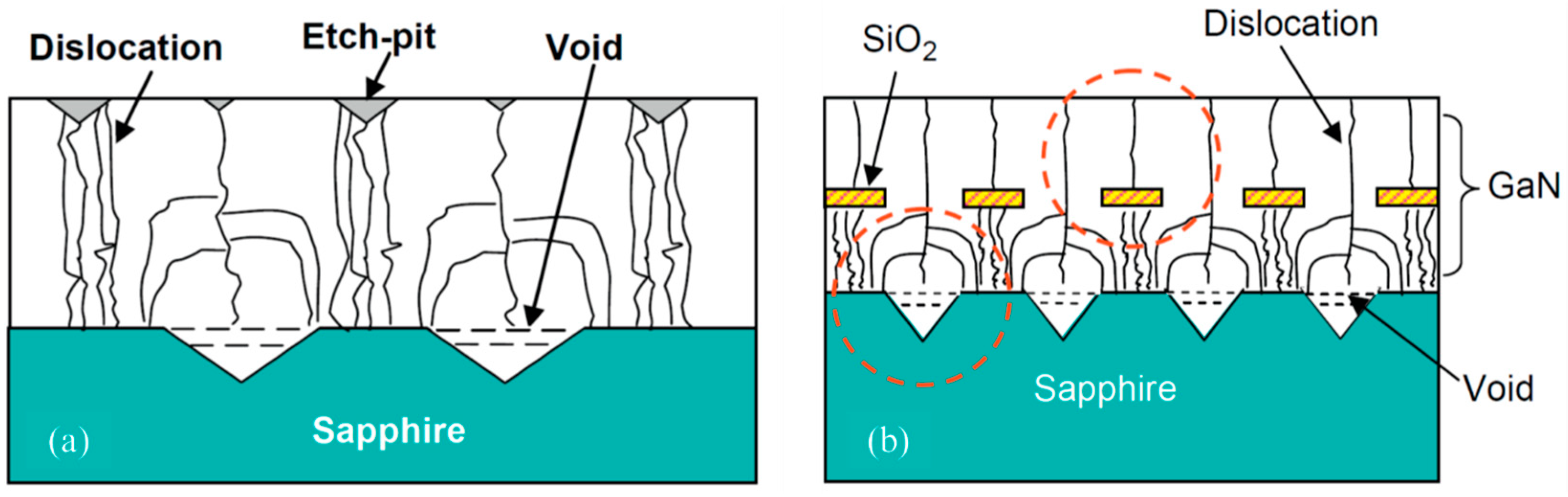
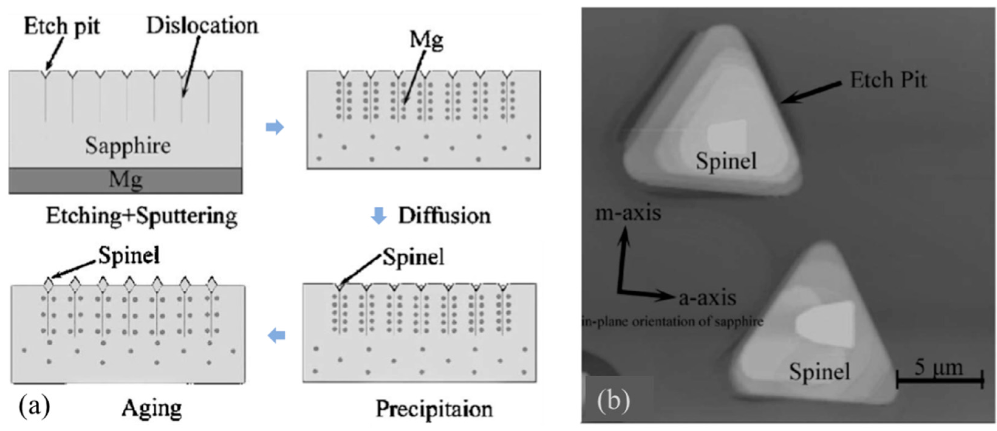
Etch pits could form on an exposed surface of a crystal when the crystal is exposed to an etching environment or chemicals. Due to different dissolution rates along various crystalline directions in a crystal, the dissolution process is anisotropic; hence, etch pits usually have a regular shape. The morphology, size, and density of etch pits can be affected by various factors, including the chemical composition of the etchant, etching time, etching temperature, status of the matrix, and so on. Traditionally, etch pits are utilized to evaluate the dislocation density and some defect-related properties. Now, in the modern fabrication industries, the relationship between etch pits and defects has been utilized more skillfully. High-quality crystals can be fabricated by controlling dislocations revealed by etch pits. Meanwhile, with the as-revealed dislocation as the diffusion path of atoms, new crystals will emerge in corresponding etch pits.

etch pit crystal dislocation orientation defects

1. Introduction

Dissolution, chemical or electrochemical reactions, can change the morphology of crystal surfaces. If some points dissolve or react preferentially on the exposed surfaces, etch pits will form.
The dissolution of a crystal has two major morphologic changes, grain rounding and etch pit formation [1]. Dissolution proceeds by both the retreat of cleavage steps and the nucleation and coalescence of etch pits [2].
Etch pits can be obtained on solids with a crystalline structure, not only on metals, alloys, ceramics, and minerals but also on other crystalline structures, such as organic compounds. For example, on an organic molecular crystal, naphthalene, well-defined etch pits will form after etching with fuming sulfuric acid for a period [3].
As the atom arrangement in a crystal is regular, the atom arrangement on a plane varies with the orientation of the plane. Hence, the dissolution rate, or etching rate, on different planes varies. Then, after etching in a certain chemical environment for a period, well-defined, regular-shaped etch pits can be obtained on crystals [4] For example, regular-shaped etch pits formed on an Fe-36 wt% Ni Invar alloy etched with a mixture containing CuSO4, HCl, and H2O [5]. These etch pits had regular shapes. Triangular, quadrilateral, and hexagonal etch pits were observed in different grains. Etch pits in an individual grain share the same shape and orientation. The shape of etch pits changes with the orientation and polarity of the basal plane [6][7].
Utilizing etch pit characterization, the relationship between different planes can be deduced. On an HCl-etched ZnO-Bi2O3 crystal, triangular-shaped etch pits aligned face to face across the inversion boundary [8]. EBSD analysis was performed and confirmed that the grain is twinned with respect to the basal plane.
The origins of etch pits on crystals have been investigated by numerous researchers [9][10][11][12]. At sites of crystal defects, there is a region with locally high surface energy, and etch pits are prone to initiate at such a position [13]. One of the most common and important origins is dislocation [14]. Formation of the dislocation-related etch pits is the result of the interaction of the dislocation stress field and the surface energy. The etching process at dislocation-related etch pits is a reverse process of crystal growth by the screw dislocation mechanism [15]. Upon etching, the crystal growth unit at the dislocation site is in high energy and prone to be etched; hence, a nonstationary nucleus for spontaneously etching begins. As time goes on, the size of the etch pits enlarges.
According to the relationship between dislocations and etch pits, etch pit observation has become one of the most useful methods to investigate dislocations in crystals [16][17][18][19][20][21][22][23] because of its merits of low cost and simple experimental procedure [24].
Etch pits reveal dislocations on an etched surface of a crystal, and then the relationship between dislocations and properties of the crystal can be estimated by etch pit observation indirectly. For example, the etch pit observation method was utilized to investigate the dislocation structure near nano indents and low-angle boundaries after uniaxial compression of the sample [25]. In addition, the type of dislocations can be distinguished by the morphology of etch pits [26][27].
Furthermore, the etch pit observation method is also frequently utilized to count the dislocation density in crystals. For samples with high dislocation density, small etch pits are preferred for an accurate determination of the overall dislocation density, as it is harder for small etch pits to merge [28]. For samples with low dislocation density, larger etch pits are preferred to distinguish different kinds of dislocations.
To count the etch pits accurately, the etching parameters should be optimized, as the morphology and density of etch pits are affected by different factors [29][30][31][32][33]. Generally, the etchant, the etching time, the etching temperature, etc. affect the etch pits on crystals. While the etch pit formation process is not bound to a manmade corrosive environment, etch pits even form on minerals naturally. Conical- or funnel-shaped etch pits were observed on the surface of weathered olivine samples [34]. On dolomite crystals, rhombohedral etch pits formed on exposed surfaces utilizing water as the etchant [2].
As dislocations have been revealed by etch pits, the control of the dislocation density becomes feasible, and this is very important for the modern electronic industry. Hence, examples are shown here to demonstrate the improvements of the application of etch pit technology. By limiting the growth of dislocations revealed by etch pits, the dislocation density of a newly grown crystal can be reduced effectively. Meanwhile, new tiny crystals can grow in etch pits. Utilizing dislocations below etch pits as a channel, some kinds of atoms in the substrate can be transported into corresponding etch pits preferentially and form new crystals. By presenting the new and skillful utilization of etch pits, it is our hope that more ingenious methods can be found to promote the application of etch pit technology as well as related modern fabrication industries.
Pitting corrosion is a typical and hazardous form of corrosion [35][36], and it occurs on some susceptible regions which dissolve faster than the rest [37][38]. An unsteady state, such as passivity breakdown, can trigger the initiation of a pit [39]. Other than ordinary pits, this study only focuses on regular-shaped etch pits, which are caused by uneven dissolution rates along various crystalline directions and initiated at defects in crystals. Meanwhile, in many circumstances, these regular-shaped etch pits are obtained intentionally, not naturally.

2. Influencing Factors for the Formation of Etch Pits

The morphology, size, and density of etch pits can be affected by various factors, including the chemical composition of the etchant, etching time, etching temperature, status of the matrix, and so on. It is important to investigate the effect of different factors on etch pits to obtain well-defined etch pits that can be utilized to reveal defects in crystals precisely.

2.1. The Etchant

The selection of proper etchants is critical to obtain well-defined etch pits on crystals. The dissolution rate of surface atoms on crystals is closely related to the type of etchants. The morphology and density of etch pits can also be affected significantly by the etchant.

2.1.1. Effect on the Morphology of Etch Pits

The etchant could affect the size of the etch pits. The Sopori etchant and the Secco etchant were utilized to etch a multi-crystalline silicon sample. Etch pits obtained with 60 s Secco etching have a size of 0.5~1 μm, while etch pits produced by Sopori have a size of 2 μm after etching for only 5 s [40].
The types of the as-revealed etch pits could vary with etchants. Some etchants are more suitable to reveal more kinds of etch pits. On a lateral epitaxial overgrowth GaN film, molten KOH revealed threading screw dislocations, while mixed HCl vapor revealed threading screw dislocations, mixed dislocations, and threading edge dislocations [41].
The nucleation and growth process of etch pits are closely related to the composition of etchants. After etching with a saturated calcite solution containing 1 mM EDTA, symmetric rhombic etch pits were observed on calcite crystals. When the etchant was changed to a flowing saturated calcite solution, etch pit nucleation and growth halted immediately. When the etchant was changed to an undersaturated calcite solution, the growth of etch pits reinitiated, and the shape of etch pits gradually changed to an asymmetric rhombus [42].
The morphology of etch pits can be affected by adding other chemicals into the etchant. After the addition of SO42− and S2O32− ions in the 1 M NaCl solution, macro etch pits with rough walls appeared, and after the addition of HSO4 ions in the 1 M NaCl solution, strip-like etch pits appeared on the Al substrate [43]. Conventional KOH etchants are not applicable to SiC with high electron concentrations, while the addition of Na2O2 to the etchant is effective in revealing threading screw dislocations, threading edge dislocations, and basal plane dislocations [44]. The addition of sulfate ions to HCl leads to the passivation of the existing etch pits and results in a more uniform etch pit structure on the aluminum foil after alternating current etching [45].
The relative content of chemicals in an etchant can affect etch pits. On GaN, pure H3PO4 results in stripe-like etch pits; a mixture that contains H3PO4 and H2SO4 results in etch pits composed of two long {101¯0} facets, and pure H2SO4 results in rhombus-like etch pits [46]. On the (100) surface of InAs, the etchant contains HCl, H2SO4, and H2O with a volume ratio of 10:m:1 (0 ≤ m ≤ 20). When m = 0, elongated hexagonal etch pits with a long axis parallel to the [11¯0] direction were observed; as m increased from 1 to 10, the shape of the etch pits changed to a quasi-rectangle, and when m = 17, rectangular etch pits were observed [47].

2.1.2. Effect on the Density of Etch Pits

The density of dislocations revealed by different etchants can be different. This is related to the fact that some etchants can reveal more kinds of dislocations than other etchants [48][49]. On a GaN film, etch pit densities revealed by molten KOH and a mixture of H3PO4 and H2SO4 were 4 × 10⁷/cm2 and 5 × 10⁸/cm2, respectively [50].

2.1.3. Effect on the Etching Rate

The etching rate could be affected by the composition of etchants [51]. The etching rate of Ga-polar on GaN crystals was 30 nm/min with H3PO4 as the etchant, while the etch rate dropped to 8 nm/min when KOH was used as the etchant [52].

2.2. The Etching Time

As the etching time increases, the size, depth, and shape of etch pits can be changed. Meanwhile, the density of etch pits can also be affected.

2.2.1. Effect on the Morphology of Etch Pits

Generally, etch pits will enlarge and deepen with increasing etching time due to the continuous dissolution of atoms on the exposed surface of the substrate, and neighboring etching pits will merge into a larger one after a period of etching [53][54]. On an organic single crystal of 2-amino 4,6-dimethyl pyrimidine 4-nitrophenol, the size of the etch pits enlarged with increasing etching time, and then the etch pits overlapped [55]. On single crystals of stearic acid, small flat-bottomed etch pits at an etching time of 5 s became large flat-bottomed etch pits at 13 s, while pyramidal etch pits became deeper and larger, and the distance between the pyramidal etch pits varied because of the inclination of dislocations [19].
The shape of the etch pits also varies with the etching time [56][57]. On the (111) face of a diamond etched with molten NaNO3, after 40 min of etching, the conical steep-sided etch pits became flat-bottomed [58]. On the (100) face of Al under an anodic pulse current in a mixture of HCl and H2SO4, only circular etch pits were observed before reaching the steady-state potential, while after dissolution at the steady-state potential, circular etch pits transformed into square etch pits [59].
Molten potassium was chosen to etch a diamond at 600 °C, and the exposed surface was determined to be {100} [60]. The etch pit size gradually increased with increasing etching time. Initially, shallow, square etch pits were observed. When the etching time reached 1 h, the corners of some etch pits were blunted. When the etching time reached 1.5 h, octagon-shaped etch pits were observed, as shown in Figure 1.
Figure 1. Morphology of the diamond {100} face after etching at 600 °C for different times: (a) 30 min; (b) 1 h; and (c) 1.5 h [60]. Reproduced with permission from Elsevier.

2.2.2. Effect on the Density of Etch Pits

The density of etch pits can increase with increasing etching time. On 4H-SiC crystals etched with KOH, as the etching time increased, etch pits increased in number, and the original etch pits increased in size, while the increased number of etch pits could be related to the fact that more dislocations were revealed gradually as some buried dislocations emerged at the continuously lowering surface [61]. On the CR-39 surface etched with a NaOH solution, etch pits could hardly be observed when the etching time was shorter than 45 min, and the etch pit density increased slightly and then saturated with the etching time; a longer etching time resulted in over-etched pits [62].

2.3. The Etching Temperature

The size, depth, shape, and density of etch pits can be affected by the etching temperature as well [63]. Hence, the etching temperature should be confined in a reasonable region to obtain well-defined etch pits.
The morphology of the etch pits formed on crystals can be affected by the etching temperature. On ScN crystals etched with a eutectic mixture of KOH and NaOH and then rinsed in HCl solution for 5 min, it was observed that after etching at 220 °C for 10 min, hexagonal and distorted square etch pits were observed; after etching at 230~240 °C for 10 min, octagon-shaped etch pits were observed; after etching at 330 °C for 5 min, square-shaped etch pits were apparent [64]. On ZnO, well-defined hexagonal etch pits were observed on the oxygen terminated face after etching at 1050 °C for 4 h in air; when the etching temperature increased to 1100 °C, gutter-shaped hollows were observed; after etching at 1150 °C, a distortion of atomic terraces emerged [65].
The etching temperature should be maintained in a reasonable region in the etching process, as under an etching temperature that is too low or too high, no etch pits could be observed. On the C-face (0001) 4H-SiC etched with chlorine trifluoride, at 573 K, no etch pit were observed, while at 623 K, 973 K, and 1073 K, etch pits were observed [66]. On the (001) face of GaAs etched with H2 plasma, when the etching temperature was 640 K, distinct etch pits with 20~50 nm diameters and 5~10 nm depths were observed; when the temperature reached 800 K, individual etch pits could hardly be seen [67]. On the {100} face of a diamond etched with molten potassium for 15 min, when the etching temperature was 600 °C, only some small and shallow etch pits were observed; when the etching temperature increased to 700 °C, large and deep etch pits with <100>-oriented edges were observed; when the etching temperature reached 800 °C, the outline of the diamond crystal was dissolved due to the high etching rate [60].

2.4. The Matrix

Etch pits preferentially initiate at sites with unevenly distributed atoms or stress. If the crystal is doped with other elements or the atom arrangement or stress distribution in the crystal is affected by factors, such as pretreatments and/or heat treatments, the morphology, distribution, or density of etch pits would be affected accordingly.
The size and shape of the etch pits and the etching rate can be affected by doping in crystals [68]. On the {111} faces of synthetic diamond crystals, the etching rate increased as the N impurity concentration increased from 1 ppm to 200 ppm, and then the etching rate subsequently decreased. Meanwhile, the etch pits with a low N content have a convex triangle shape, while etch pits on nitrogen-doped crystals were found to be regular triangular [69].
Some etching processes contain multiple steps, including a pretreatment process. The effect of chemical pretreatment of the Al substrate on the electrochemically etched surface of Al was investigated [70]. The results show that a two-step pretreatment with H3PO4 and H2SiF6 led to a high density of pre-etch pits on the Al surface. During the subsequent electrochemical etching, a high density of etch pits was observed.
Etch pits can be affected by the heat treatments of the matrix. As it is well known that heat treatment can affect dislocations in the matrix, the variation in the etch pits before and after heat treatment can be related to the variation in dislocations in the matrix. The etch pit variation before and after a heat treatment of a HgCdTe matrix was investigated [71]. After annealing for 4 cycles at 494 °C, there was a nonuniform reduction in the dislocation density identified by etch pit observation; meanwhile, the fish-shaped etch pits were completely absent.

2.5. Electrochemical Parameters

Etch pits can also be obtained by electrochemical etching; hence, electrochemical parameters also affect the etch pits on crystals. Anodic etching was carried out to obtain etch pits on GaN films [72]. When the electrolysis voltage was 50 V and 30 V, the surface was over-etched; when the voltage was 20 V, the etch pits were observed; when the voltage was 10 V, the etch pits could also be observed, but the density was lower. An Al substrate was etched in a HCl-H2SO4 solution with different current profiles including the direct current, anodic pulse, and square wave, only square waves produced cubic etch pits [73].

2.6. The Atmosphere

As the formation of etch pits is determined by the dissolution or chemical reactions of the surface atoms of crystals and the dissolution and chemical reactions can be affected by the chemical environment; hence, etch pits can also be affected by the chemical environment, including the atmosphere. Many gases are effective etchants to obtain etch pits on crystals.
Atomic hydrogen was utilized to etch epitaxial diamond (111) films [74]. After exposure to atomic hydrogen for 12 min at 500 °C, square pits with (111)-oriented facets were observed. After exposure to oxygen at 1 × 10⁻³ Torr for 1 min at room temperature and then exposure to atomic hydrogen at 500 °C for 5 min again, new etch pits were formed, and these new pits were inferred to be related to oxidation.
After exposure to ambient humidity, etch pits formed on potassium dihydrogen phosphate crystals with porous coatings [75]. The shapes of the etch pits were regular. At 10% RH, the etch pits were 0.5~1 μm in length; at 55% RH, the average length of the etch pits was 3.5 ± 0.5 μm; at 75% RH, the etch pits grew to 20 μm. When the RH increased from 10% to 75%, the etch pit density decreased by two orders of magnitude.

2.7. Other Factors

There are other factors that can affect the formation of etch pits on crystals, such as catalysts [76], magnetic fields [77], and illumination [78]. Catalysts can affect chemical reactions on the surface of crystals. The magnetic field can act on the ions in the liquid in the etch pit and affect the transport of reactants and products of chemical reactions. In the n-type material, light could not only speed up the reaction rate but also reveal the defects as crystallographic defects are effective sites for the recombination of photogenerated carriers [78].
A highly {110}-oriented diamond coating was etched with hydrogen gas with Fe, Co, Ni and Pt nanoparticles as catalysts [76]. The metal atoms were vacuum-evaporated onto the diamond coating and formed nanoparticles by themselves at an elevated temperature. The samples were kept in a flowing gas mixed with H2 (10%) and N2 (90%) between 700 °C and 1000 °C for a specific duration. Co was preferred by the etching process carried out at 800 °C for 2 h, as dense etch pits were observed. When Pt was utilized as the catalyst, it was difficult to identify the etch pits after etching at 900 °C.

3. Applications of Etch Pit Technology

In the beginning of the 19th century, etch pit technology had already been utilized to investigate crystals [79]. It is well known that the properties of a crystal and/or a multi-crystalline substrate are closely related to the intrinsic defects in the crystal and/or the multi-crystalline substrate. For example, the dislocation slip and the deformation twinning are the most common deformation mechanisms in coarse-grained materials. Dislocations can nucleate and slip under stress to accommodate the applied plastic deformation, while dislocation entanglement and accumulation will consequently lead to strain hardening [80]. As defects can be revealed by etch pits, it is meaningful to utilize etch pits to evaluate and even improve some key properties of the matrix, as shown in Figure 2.
Figure 2. Schematic diagram of the relationship of etch pits, defects, and properties.

3.1. Investigation of Dislocations

Due to the relationship between dislocations and etch pits, etch pit observation is frequently employed to characterize, evaluate, and count dislocations in crystals [18][31]. In the middle of the 20th century, researchers had already revealed dislocations with etch pits deliberately [81].
The distribution of dislocations can be revealed by etch pits [82][83]. Polishing and etching could be carried out several times to trace the dislocation lines at different depths in an identical specimen [84]. As a relatively larger area can be etched with etchants, the distribution of dislocations can be identified in a relatively macroscopic manner [85] compared to those revealed by transmission electron microscope.
Etch pit observation can be utilized to investigate an individual dislocation or compare dislocations in different substrates. On the (111) face of CdZnTe, the orientations of dislocations related to the triangular etch pits were determined by measuring the depths of the etch pits, the orientations of the etch pit tips, and the side lengths of the triangular etch pits [86]. The density of non-basal dislocations on the (001) face of anthracene was found to be larger in an annealed crystal than in an unannealed crystal [87].

3.2. Reduction of Dislocations

As etch pits have already revealed many emergences of dislocations, in the following growth process of a new crystal upon a pre-etched crystal, it is important to confine the extension of the as-revealed dislocations, so that a low dislocation density crystal can be obtained.
Pits can be utilized to reduce the dislocation density in a newly formed crystal; as in the growing process of crystals on pits, dislocations tend to merge [88]. A recess-patterned sapphire substrate and a protruding sapphire substrate were prepared utilizing a SiO2 mask [89], and the recess-patterned sapphire substrate was proven to be better since the density of dislocations was relatively smaller, as shown in Figure 3.
Figure 3. Reduction in dislocations by pits (a) and the combination of pits and an oxide mask (b) [89]. Reproduced with permission from Elsevier.
Then, as a typical kind of pit, etch pits were utilized directly to reduce dislocations [90]. On a GaN substrate with several large and deep etch pits, a new bulk GaN with low dislocation density was obtained by hydride vapor phase epitaxy [91]. A Ge film with a threading dislocation density of 2.6 × 108 cm−2 was etched to produce etch pits, and then a 15 nm thick SiO2 film was utilized to cover the etch pits. The subsequent growth resulted in a Ge epilayer with a threading dislocation density of 1.7 × 106 cm−2 [92].

3.3. Count of Precipitates

The areal defect densities caused by the precipitates on the surface of CdZnTe could be measured by etch pit observation [93]. Etch pits caused by the Te-rich precipitate and Cd-rich precipitate were different. The former etch pits were crater-like, and the latter etch pits were always enwrapped by many other etch pits. The areal densities obtained by etch pit observation were consistent with those obtained by IR transmission microscopy, while the etch pit observation method saves time, and only one side of the specimen needs to be polished.

3.4. Polytype Identification

Polytypes of SiC could be identified by etch pit observation [94]. SiC crystals with perfect hexagonal etch pits were 6H-SiC along the (0001) direction, and the SiC crystals with three long-edge and three short-edge hexagonal etch pits were 15R-SiC along the (0001) direction. This relationship was verified by the Raman spectra.

3.5. Polarity Detemination

The polarity of InN can be identified by etch pit observation [95]. After etching with KOH, hexagonal pyramids surrounded by {101¯1¯} facets were observed on the N-polar surface, while hexagonal and dot-shaped etch pits were observed on the In-polar surface. Meanwhile, the dislocation density identified by the etch pit density on the In-polar surface almost corresponded to the threading dislocation density determined by transmission electron microscopy.

3.6. Detection of Leakage Current

The relationship between crystal defects and leakage current can be determined via etch pit observation. On β-Ga2O3 Schottky barrier diodes, dislocations and voids were revealed by etch pits after etching, and a comparison between the leakage current and the crystal defects indicated that dislocations along [010] acted as paths for the leakage current [96]. In a GaN-based light-emitting device, the origin of the leakage current was also investigated by etch pit observation, and the leakage current was attributed to open core dislocations [97].

4. Trends Related to Etch Pit Technology

4.1. Characterization of Etch Pits

Usually, etch pits are characterized by an optical microscope, a scanning electron microscope, or an atomic force microscope, and these etch pits are usually analyzed by manually interpreting the photographs of etch pits. To improve the efficiency of the interpretation process, new methods have been developed.
The etch pit density can be counted and/or analyzed utilizing a software [98]. Kanik Palodhi et al. [99] utilized an image processing technique based on convolution to analyze etch pits on nuclear track detectors, and this approach substantially sped up the task of track identification and analysis. M. Wzorek et al. [100] proposed a method that implements a shape-from-shading method to estimate the depths of etch pits by analyzing the image brightness dependence on the slopes of etch pits, and the depth distribution revealed etch pits attributed to different kinds of dislocations in a GaN substrate. The ratio of different kinds of dislocations estimated by this method is comparable to that obtained by transmission electron microscopy.
Furthermore, a dissolution process can be measured by the phase shifting interferometry (PSI) approach. A.E.S. Van Driessche et al. utilized a white beam PSI [101] to characterize the variation in the morphology of etch pits on a gypsum crystal [102].
As the size, morphology, and density of etch pits vary with etching time, it is important to characterize the etch pits in-situ to further understand the growth process of the etch pits. Fuminobu Sato et al. [103] recorded time-lapse images of etch pits formed on a nuclear track detector by an in-situ observation system, and then the pit evolution images were constructed by digital image processing of the time-lapse images.

4.2. Simulation of Disolution

As it is difficult to characterize the initiation and expansion of an etch pit in-situ on the atomic scale, it is critical to simulate these processes for a deeper understanding. Inna Kurganskaya et al. [104] utilized a stochastic Kinetic Monte Carlo approach to describe the dissolution of phyllosilicates and predicted the surface evolution from the kinetics of elementary surface reactions and found that the dissolution of minerals proceeds via the formation of etch pits at opened screw dislocation cores through movement and coalescence of step waves. Konstanze Stübner et al. [105] simulated the evolution of etch pits with an atomistic Monte Carlo simulation, and the results suggested that there are four stages in the evolution of etch pits on the (001) surface of an idealized regular lattice. During the first stage, an etch pit was an inverted pyramid. Then, the pyramid apex was truncated in the second stage. During the third stage, an etch pit consisted of a single concave up bottom plane. During the fourth stage, it was inferred that the etch pits would shrink until they disappeared altogether.

4.3. Etching on Macro Patterns

Usually, to statistically obtain the distribution of etch pits or other defects on an exposed surface, a sufficiently large surface area should be etched. It is also possible to etch partial areas or patterned areas of an exposed surface of a crystal for some purposes. Sachiko Ono et al. [106] utilized a honeycomb Al2O3 mask to directly control the initial sites of etch pits; hence, the distribution, density, and homogeneity of the etch pits were adjusted. Dmitri A Brevnov et al. [107] utilized Al2O3 as the etching mask and carried out electrochemical etching on Al (100) foils. Then, crystallographic cubic etch pits were observed at the unmasked area, and the Al substrate was preserved at the masked region.

4.4. Self-Assemble of Particles at Etch Pits

An etch pit could be a container for other materials. Because of the regular shape of etch pits, extrinsic substances could gather at positions preferentially in the etch pits. Hung-Ming Chen et al. [108] investigated the effect of etch pits on the alignment of Ge dots grown on a pit-patterned Si (001) substrate. When the spacing between the etch pits was less than 100 nm and the depth of the etch pits was greater than 60 nm, the topology and the surface chemical distribution were favored by Ge dots to nucleate inside the pits and completely align with each other.

4.5. Crystal Growth at Etch Pits

A dislocation can be revealed by an etch pit, and the as-revealed dislocation is a shortcut for some kinds of atoms to transport. The aggregation of the transported atoms in the etch pits can result in a new crystal. Che-Ming Liu et al. [109] pointed out that etch pits are preferred sites for crystal growth. One side of a sapphire crystal was etched with Na2B4O7, and etch pits were obtained. Then, a Mg film was deposited on the unpolished surface. After heating and aging of the specimen, precipitation crystals were found at the etch pits of the sapphire as shown in Figure 4. These newly formed crystals are Mg-Al spinel microcrystals.
Figure 4. Schematic diagram of the fabrication process (a) and the as-fabricated spinels (b) [109]. Reproduced with permission from AIP Publishing.

References

  1. Gautier, J.M.; Oelkers, E.H.; Schott, J. Are quartz dissolution rates proportional to B.E.T. surface areas? Geochim. Cosmochim. Acta 2001, 65, 1059–1070.
  2. Pina, C.M.; Pimentel, C.; García-Merino, M. High resolution imaging of the dolomite (104) cleavage surface by atomic force microscopy. Surf. Sci. 2010, 604, 1877–1881.
  3. Mercier, M.; Raimi, M.K.; Bonpunt, L. Observation by transmission electron microscopy of etch figures obtained on an organic molecular crystal. Microsc. Res. Tech. 1992, 21, 53–58.
  4. Saito, K.; Sugawara, S.; Sato, T.; Guo, J.Q.; Tsai, A.P. Unique shapes of micro-pits formed in an Al-Pd-Mn icosahedral quasicrystal by anodic etching. Mater. Trans. JIM 2000, 41, 1221–1225.
  5. Lu, D.Z.; Wu, M.J. Observation of etch pits in Fe-36wt%Ni Invar alloy. Int. J. Miner. Metall. Mater. 2014, 21, 682–686.
  6. Bondokov, R.T.; Mueller, S.G.; Morgan, K.E.; Slack, G.A.; Schujman, S.; Wood, M.C.; Smart, J.A.; Schowalter, L.J. Large-area AlN substrates for electronic applications: An industrial perspective. J. Cryst. Growth 2008, 310, 4020–4026.
  7. He, Z.; Zhao, B.; Zhu, S.; Chen, B.; Huang, W.; Lin, L.; Feng, B. Crystal growth and dislocation etch pits observation of chalcopyrite CdSiP2. J. Cryst. Growth 2018, 481, 29–34.
  8. Jo, W.; Kim, S.J.; Kim, D.Y. Analysis of the etching behavior of ZnO ceramics. Acta Mater. 2005, 53, 4185–4188.
  9. Chen, J.; Wang, J.F.; Wang, H.; Zhu, J.J.; Zhang, S.M.; Zhao, D.G.; Jiang, D.S.; Yang, H.; Jahn, U.; Ploog, K.H. Measurement of threading dislocation densities in GaN by wet chemical etching. Semicond. Sci. Technol. 2006, 21, 1229–1235.
  10. Chaudhuri, J.; Lee, R.G.; Nyakiti, L.; Armstrong, J.; Gu, Z.; Edgar, J.H.; Wen, J.G. Transmission electron microscopy study of defect-selective etched (010) ScN crystals. Mater. Lett. 2008, 62, 27–29.
  11. Zeng, D.; Jie, W.; Wang, T.; Zhang, J.; Zha, G. Type and formation mechanism of thermal etch pit on annealed (111) CdZnTe surface. Thin Solid Films 2009, 517, 2896–2899.
  12. Vaghayenegar, M.; Jacobs, R.N.; Benson, J.D.; Stoltz, A.J.; Almeida, L.A.; Smith, D.J. Correlation of Etch Pits and Dislocations in As-grown and Thermal Cycle-Annealed HgCdTe(211) Films. J. Electron. Mater. 2017, 46, 5007–5019.
  13. Adkins, J.F.; Naviaux, J.D.; Subhas, A.V.; Dong, S.; Berelson, W.M. The Dissolution Rate of CaCObinf3einf in the Ocean. Annu. Rev. Mar. Sci. 2021, 13, 57–80.
  14. Hino, T.; Tomiya, S.; Miyajima, T.; Yanashima, K.; Hashimoto, S.; Ikeda, M. Characterization of threading dislocations in GaN epitaxial layers. Appl. Phys. Lett. 2000, 76, 3421–3423.
  15. Xu, L.; Yu, B.; Yu, G.; Liu, H.; Zhang, L.; Li, X.; Huang, P.; Wang, B.; Wang, S. Study on the morphology of dislocation-related etch pits on pyramidal faces of KDP crystals. CrystEngComm 2021, 23, 2556–2562.
  16. Yang, J.R.; Cao, X.L.; Wei, Y.F.; He, L. Traces of HgCdTe defects as revealed by etch pits. J. Electron. Mater. 2008, 37, 1241–1246.
  17. Lantreibecq, A.; Legros, M.; Plassat, N.; Monchoux, J.P.; Pihan, E. Spatial distribution of structural defects in Cz-seeded directionally solidified silicon ingots: An etch pit study. J. Cryst. Growth 2018, 483, 183–189.
  18. Corke, N.T.; Kawada, A.A.; Sherwood, J.N. Etching of Dislocations in Crystals of Aromatic Hydrocarbons. Nature 1967, 213, 62–63.
  19. Sato, K.; Okada, M. Etching on large single crystals of stearic acid. Nature 1977, 269, 399–400.
  20. Mukerji, S.; Kar, T. Etch pit study of different crystallographic faces of L-arginine hydrobromide monohydrate (LAHBr) in some organic acids. J. Cryst. Growth 1999, 204, 341–347.
  21. Hashimoto, T.; Wu, F.; Speck, J.S.; Nakamura, S. A GaN bulk crystal with improved structural quality grown by the ammonothermal method. Nat. Mater. 2007, 6, 568–571.
  22. Kawamura, F.; Tanpo, M.; Miyoshi, N.; Imade, M.; Yoshimura, M.; Mori, Y.; Kitaoka, Y.; Sasaki, T. Growth of GaN single crystals with extremely low dislocation density by two-step dislocation reduction. J. Cryst. Growth 2009, 311, 3019–3024.
  23. Benson, J.D.; Smith, P.J.; Jacobs, R.N.; Markunas, J.K.; Jaime-Vasquez, M.; Almeida, L.A.; Stoltz, A.; Bubulac, L.O.; Groenert, M.; Wijewarnasuriya, P.S.; et al. Topography and dislocations in (112)B HgCdTe/CdTe/Si. J. Electron. Mater. 2009, 38, 1771–1775.
  24. Lu, L.; Gao, Z.Y.; Shen, B.; Xu, F.J.; Huang, S.; Miao, Z.L.; Hao, Y.; Yang, Z.J.; Zhang, G.Y.; Zhang, X.P.; et al. Microstructure and origin of dislocation etch pits in GaN epilayers grown by metal organic chemical vapor deposition. J. Appl. Phys. 2008, 104, 123525.
  25. Sadrabadi, P.; Durst, K.; Goken, M.; Blum, W. Quantification of dislocation structures at high resolution by atomic force microscopy of dislocation etch pits. Philos. Mag. Lett. 2009, 89, 391–398.
  26. Hatayama, T.; Shimizu, T.; Kouketsu, H.; Yano, H.; Uraoka, Y.; Fuyuki, T. Thermal etching of 4H-SiC(0001) Si faces in the mixed gas of chlorine and oxygen. Jpn. J. Appl. Phys. 2009, 48, 066516.
  27. Kallinger, B.; Polster, S.; Berwian, P.; Friedrich, J.; Mller, G.; Danilewsky, A.N.; Wehrhahn, A.; Weber, A.D. Threading dislocations in n- and p-type 4HSiC material analyzed by etching and synchrotron X-ray topography. J. Cryst. Growth 2011, 314, 21–29.
  28. Habel, F.; Seyboth, M. Determination of dislocation density in epitaxially grown GaN using an HCl etching process. Phys. Status Solidi C Conf. 2003, 2451, 2448–2451.
  29. Shah, I.A.; van der Wolf, B.M.A.; van Enckevort, W.J.P.; Vlieg, E. Wet chemical etching of silicon : Etch pit analysis by the Lichtfigur method. J. Cryst. Growth 2009, 311, 1371–1377.
  30. Shah, I.A.; van der Wolf, B.M.A.; van Enckevort, W.J.P.; Vlieg, E. Wet Chemical Etching of Silicon : Autocatalysis in Pit Formation. J. Electrochem. Soc. 2008, 155, J79.
  31. Bickermann, M.; Schmidt, S.; Epelbaum, B.M.; Heimann, P.; Nagata, S.; Winnacker, A. Wet KOH etching of freestanding AlN single crystals. J. Cryst. Growth 2007, 300, 299–307.
  32. Fleck, M.; Zuschlag, A.; Hahn, G. Etch Pit Density Reduction in POCl3 and Atmospheric Pressure Chemical Vapor Deposition-Gettered mc-Si. Phys. Status Solidi Appl. Mater. Sci. 2019, 216, 1900316.
  33. Persichetti, L.; Fanfoni, M.; De Seta, M.; Di Gaspare, L.; Ottaviano, L.; Goletti, C.; Sgarlata, A. Formation of extended thermal etch pits on annealed Ge wafers. Appl. Surf. Sci. 2018, 462, 86–94.
  34. Velbel, M.A. Dissolution of olivine during natural weathering. Geochim. Cosmochim. Acta 2009, 73, 6098–6113.
  35. Bhandari, J.; Khan, F.; Abbassi, R.; Garaniya, V.; Ojeda, R. Modelling of pitting corrosion in marine and offshore steel structures—A technical review. J. Loss Prev. Process Ind. 2015, 37, 39–62.
  36. Xu, W.; Zhang, B.; Deng, Y.; Wang, Z.; Jiang, Q.; Yang, L.; Zhang, J. Corrosion of rail tracks and their protection. Corros. Rev. 2021, 39, 1–13.
  37. Frankel, G.S. Pitting Corrosion of Metals. Corrosion 1998, 145, 2186–2198.
  38. Campbell, J. The Mechanisms of Metallurgical Failure The origin of Fracture; Matthew Deans: Oxford, UK, 2020.
  39. Soltis, J. Passivity breakdown, pit initiation and propagation of pits in metallic materials—Review. Corros. Sci. 2015, 90, 5–22.
  40. Adamczyk, K.; Stokkan, G.; Di Sabatino, M. Guidelines for establishing an etching procedure for dislocation density measurements on multicrystalline silicon samples. MethodsX 2018, 5, 1178–1186.
  41. Lu, M.; Chang, X.; Li, Z.L.; Yang, Z.J.; Zhang, G.Y.; Zhang, B. Etch pits and threading dislocations in GaN films grown by metal-organic chemical vapour deposition. Chin. Phys. Lett. 2003, 20, 398–400.
  42. Britt, D.W.; Hlady, V. In-situ atomic force microscope imaging of calcite etch pit morphology changes in undersaturated and 1-hydroxyethylidene-1,1-diphosphonic acid poisoned solutions. Langmuir 1997, 13, 1873–1876.
  43. Na, K.H.; Pyun, S. Il Effects of SO42−, S2O32− and HSO4− Ion additives on the pitting corrosion of pure aluminium in 1 M NaCl solution at 40–70 °C. J. Solid State Electrochem. 2005, 9, 639–645.
  44. Yao, Y.-Z.; Ishikawa, Y.; Sugawara, Y.; Saitoh, H.; Danno, K.; Suzuki, H.; Kawai, Y.; Shibata, N. Molten KOH Etching with Na2O2 Additive for Dislocation Revelation in 4H-SiC Epilayers and Substrates. Jpn. J. Appl. Phys. 2011, 50, 075502.
  45. Lin, C.S.; Li, W.J. Pitting Behavior of Aluminum Foil during Alternating Current Etching in Hydrochloric Acid Containing Sulfate Ions. J. Electrochem. Soc. 2006, 153, C51.
  46. Hsu, H.C.; Su, Y.K.; Cheng, S.H.; Huang, S.J.; Cao, J.M.; Chen, K.C. Investigation of etch characteristics of non-polar GaN by wet chemical etching. Appl. Surf. Sci. 2010, 257, 1080–1083.
  47. Shen, G.; Zhao, Y.; Sun, J.; Liu, J.; Xie, H.; Yang, J.; Dong, Z. HCl-H2SO4-H2O solution etching behavior of InAs (1 0 0) surface. J. Cryst. Growth 2020, 547, 125800.
  48. Jianrong, Y.; Huiming, G.; Xinqiang, C.; Weizheng, F.; Li, H. Dislocation assessment of CdZnTe by chemical etching on both (1 1 1)B and (2 1 1)B faces. J. Cryst. Growth 2002, 234, 337–342.
  49. Zhang, L.; Shao, Y.; Wu, Y.; Hao, X.; Chen, X.; Qu, S.; Xu, X. Characterization of dislocation etch pits in HVPE-grown GaN using different wet chemical etching methods. J. Alloys Compd. 2010, 504, 186–191.
  50. Min, L.; Xin, C.; Hui-Zhi, F.; Zhi-Jian, Y.; Hua, Y.; Zi-Lan, L.; Qian, R.; Guo-Yi, Z.; Bei, Z. Etch-pits and threading dislocations in thick LEO GaN films on sapphire grown by MOCVD. Phys. Status Solidi C Conf. 2004, 1, 2438–2440.
  51. Karan, S.; Sen Gupta, S.; Sen Gupta, S.P. Revelation of dislocation etch pits in mixed crystals of ammonium-potassium sulphate, 2SO4. J. Cryst. Growth 2001, 233, 555–560.
  52. Han, S.-C.; Kim, J.-K.; Kim, J.Y.; Kim, K.-K.; Tampo, H.; Niki, S.; Lee, J.-M. Formation of Hexagonal Pyramids and Pits on V-/VI-Polar and III-/II-Polar GaN/ZnO Surfaces by Wet Etching. J. Electrochem. Soc. 2010, 157, D60.
  53. Tiwari, R.N.; Chang, L. Etching of GaN by microwave plasma of hydrogen. Semicond. Sci. Technol. 2010, 25, 035010.
  54. Wang, K.S.; Resch, R.; Dunn, K.; Shuler, P.; Tang, Y.; Koel, B.E.; Yen, T.F. Scanning force microscopy study of etch pits formed during dissolution of a barite (001) surface in CDTA and EDTA solutions. Langmuir 2000, 16, 649–655.
  55. Karuppasamy, P.; Kamalesh, T.; Anitha, K.; Abdul Kalam, S.; Senthil Pandian, M.; Ramasamy, P.; Verma, S.; Venugopal Rao, S. Synthesis, crystal growth, structure and characterization of a novel third order nonlinear optical organic single crystal: 2-Amino 4,6-Dimethyl Pyrimidine 4-nitrophenol. Opt. Mater. 2018, 84, 475–489.
  56. Hanada, K.; Moribayashi, T.; Koshi, K.; Sasaki, K.; Kuramata, A.; Ueda, O.; Kasu, M. Origins of etch pits in β-Ga2O3(010) single crystals. Jpn. J. Appl. Phys. 2016, 55, 1202BG.
  57. Osawa, N.; Fukuoka, K. Pit nucleation behavior of aluminium foil for electrolytic capacitors during early stage of DC etching. Corros. Sci. 2000, 42, 585–597.
  58. Khokhryakov, A.F.; Palyanov, Y.N. Revealing of dislocations in diamond crystals by the selective etching method. J. Cryst. Growth 2006, 293, 469–474.
  59. Ono, S.; Habazaki, H. Pit growth behaviour of aluminium under galvanostatic control. Corros. Sci. 2011, 53, 3521–3525.
  60. Li, L.; Chen, X.; Zhang, W.; Peng, K. Characterization and formation mechanism of pits on diamond face etched by molten potassium nitrite. Int. J. Refract. Met. Hard Mater. 2018, 71, 129–134.
  61. Cui, Y.; Hu, X.; Xie, X.; Xu, X. Threading dislocation classification for 4H-SiC substrates using the KOH etching method. CrystEngComm 2018, 20, 978–982.
  62. Yasuda, N.; Koguchi, Y.; Tsubomatsu, M.; Takagi, T.; Kobayashi, I.; Tsuruta, T.; Morishima, H. Extremely high dose neutron dosimetry using CR-39 and atomic force microscopy. Radiat. Prot. Dosim. 2006, 120, 470–474.
  63. Kachroo, S.K.; Bamzai, K.K.; Dhar, P.R.; Kotru, P.N.; Wanklyn, B.M. Etch patterns on flux grown DyFeO3 crystal surfaces. Mater. Chem. Phys. 2001, 68, 72–76.
  64. Gu, Z.; Edgar, J.H.; Coffey, D.W.; Chaudhuri, J.; Nyakiti, L.; Lee, R.G.; Wen, J.G. Defect-selective etching of scandium nitride crystals. J. Cryst. Growth 2006, 293, 242–246.
  65. Petukhov, V.; Bakin, A.; El-Shaer, A.H.; Mofor, A.C.; Waag, A. Etch-pit density investigation on both polar faces of ZnO substrates. Electrochem. Solid-State Lett. 2007, 10, H357.
  66. Habuka, H.; Fukumoto, Y.; Kato, T. Off-Orientation Influence on C-Face (0001) 4H-SiC Surface Morphology Produced by Etching Using Chlorine Trifluoride Gas. ECS J. Solid State Sci. Technol. 2013, 2, N3025–N3027.
  67. Robey, S.W.; Sinniah, K. Initial etching of GaAs (001) during plasma cleaning. J. Appl. Phys. 2000, 88, 2994–2998.
  68. Wu, P. Etching study of dislocations in heavily nitrogen doped SiC crystals. J. Cryst. Growth 2010, 312, 1193–1198.
  69. Khokhryakov, A.F.; Palyanov, Y.N. Effect of nitrogen impurity on etching of synthetic diamond crystals. J. Cryst. Growth 2015, 430, 71–74.
  70. Lee, J.; Kim, J.; Kim, J.; Lee, J.; Chung, H.; Tak, Y. Effects of pretreatment on the aluminium etch pit formation. Corros. Sci. 2009, 51, 1501–1505.
  71. Farrell, S.; Rao, M.V.; Brill, G.; Chen, Y.; Wijewarnasuriya, P.; Dhar, N.; Benson, J.D.; Harris, K. Comparison of the schaake and benson etches to delineate dislocations in HgCdTe layers. J. Electron. Mater. 2013, 42, 3097–3102.
  72. Sundararajan, S.P.; Crouse, D.; Lo, Y.-H. Gallium nitride: Method of defect characterization by wet oxidation in an oxalic acid electrolytic cell. J. Vac. Sci. Technol. B Microelectron. Nanom. Struct. 2002, 20, 1339.
  73. Ono, S.; Habazaki, H. Role of cathodic half-cycle on AC etch process of aluminium. Corros. Sci. 2010, 52, 2164–2171.
  74. Stallcup, R.E.; Mo, Y.; Scharf, T.W.; Perez, J.M. Formation of nanometer-size high-density pits on epitaxial diamond (100) films. Diam. Relat. Mater. 2007, 16, 1727–1731.
  75. Wheeler, E.K.; Whitman, P.K.; Land, T.A.; De Yoreo, J.; Thorsness, C.B.; McWhirter, J.H.; Hanna, M.L.; Miller, E.L. Investigation of etch pits on KDP crystals with porous sol-gel coatings. Appl. Phys. A Mater. Sci. Process. 2002, 74, 813–823.
  76. Ohashi, T.; Sugimoto, W.; Takasu, Y. Catalytic etching of -oriented diamond coating with Fe, Co, Ni, and Pt nanoparticles under hydrogen. Diam. Relat. Mater. 2011, 20, 1165–1170.
  77. Ivashchenko, V.E.; Boldyrev, V.V.; Zakharov, Y.A.; Shakhtshneider, T.P.; Ermakov, A.E.; Krasheninin, V.I. The effect of magnetic field on the shape of etch pits of paracetamol crystals. Mater. Res. Innov. 2002, 5, 214–218.
  78. Weyher, J.L. Characterization of Compound Semiconductors by Etching. In Concise Encyclopedia of Semiconducting Materials & Related Technologies; Pergamon: Oxford, UK, 1992; pp. 37–44.
  79. McDougall, D.J. Etch pits. In Mineralogy; Frye, K., Ed.; Springer: Boston, MA, USA, 1983; pp. 150–152.
  80. Cao, Y.; Ni, S.; Liao, X.; Song, M.; Zhu, Y. Structural evolutions of metallic materials processed by severe plastic deformation. Mater. Sci. Eng. R Rep. 2018, 133, 1–59.
  81. Gale, W.F.; Totemeier, T.C. (Eds.) Smithells Metals Reference Book; Elsevier: Oxford, UK, 2004; p. 26.
  82. Nicolov, M. Shaped single crystals of CaF2. J. Cryst. Growth 2000, 218, 62–66.
  83. Javaid, F.; Bruder, E.; Durst, K. Indentation size effect and dislocation structure evolution in (001) oriented SrTiO3 Berkovich indentations: HR-EBSD and etch-pit analysis. Acta Mater. 2017, 139, 1–10.
  84. Hossain, A.; Bolotnikov, A.E.; Camarda, G.S.; Cui, Y.; Yang, G.; James, R.B. Defects in cadmium zinc telluride crystals revealed by etch-pit distributions. J. Cryst. Growth 2008, 310, 4493–4498.
  85. Yao, Y.; Sugawara, Y.; Ishikawa, Y.; Okada, N.; Tadatomo, K. Crystallinity Evaluation and Dislocation Observation for an Aluminum Nitride Single-Crystal Substrate on a Wafer Scale. J. Electron. Mater. 2020, 49, 5144–5153.
  86. Cui, X.P.; Fang, W.Z.; Sun, S.W.; Zhang, C.J.; Xu, H.L.; Yang, J.R. Characteristics of the dislocations in CdZnTe crystals revealed by etch pits. J. Cryst. Growth 2011, 321, 40–44.
  87. Lisovenko, V.A.; Khutornaya, L.A.; Shpak, M.T.; Velikaya, E.N. Basal dislocations in anthracene crystals. Phys. Status Solidi 1977, 42, 433–437.
  88. Motoki, K.; Okahisa, T.; Nakahata, S.; Matsumoto, N.; Kimura, H.; Kasai, H.; Takemoto, K.; Uematsu, K.; Ueno, M.; Kumagai, Y.; et al. Preparation of large GaN substrates. Mater. Sci. Eng. B Solid-State Mater. Adv. Technol. 2002, 93, 123–130.
  89. Wuu, D.S.; Wu, H.W.; Chen, S.T.; Tsai, T.Y.; Zheng, X.; Horng, R.H. Defect reduction of laterally regrown GaN on GaN/patterned sapphire substrates. J. Cryst. Growth 2009, 311, 3063–3066.
  90. Hu, W.; Die, J.; Wang, C.; Yan, S.; Hu, X.; Du, C.; Jiang, Y.; Deng, Z.; Wang, L.; Jia, H.; et al. The substantial dislocation reduction by preferentially passivating etched defect pits in GaN epitaxial growth. Appl. Phys. Express 2019, 12, 035502.
  91. Lee, M.; Mikulik, D.; Yang, M.; Park, S. Nearly perfect GaN crystal via pit-assisted growth by HVPE. CrystEngComm 2017, 19, 2036–2041.
  92. Leonhardt, D.; Han, S.M. New Method to Produce High-Quality Epitaxial Ge on Si Using SiO2-Lined Etch Pits and Epitaxial Lateral Overgrowth for III-V Integration. ECS Trans. 2012, 45, 147–149.
  93. Sheng, F.F.; Cui, X.P.; Sun, S.W.; Yang, J.R. Etch pits of precipitates in CdZnTe crystals on (1 1 1) B surface. J. Cryst. Growth 2012, 354, 76–80.
  94. Yang, Y.; Chen, Z. Identification of SiC polytypes by etched Si-face morphology. Mater. Sci. Semicond. Process. 2009, 12, 113–117.
  95. Muto, D.; Araki, T.; Naoi, H.; Matsuda, F.; Nanishi, Y. Polarity determination of InN by wet etching. Phys. Status Solidi Appl. Mater. Sci. 2005, 202, 773–776.
  96. Kasu, M.; Hanada, K.; Moribayashi, T.; Hashiguchi, A.; Oshima, T.; Oishi, T.; Koshi, K.; Sasaki, K.; Kuramata, A.; Ueda, O. Relationship between crystal defects and leakage current in β-Ga2O3 Schottky barrier diodes. Jpn. J. Appl. Phys. 2016, 55, 1202BB.
  97. Lee, S.W.; Oh, D.C.; Goto, H.; Ha, J.S.; Lee, H.J.; Hanada, T.; Cho, M.W.; Yao, T.; Hong, S.K.; Lee, H.Y.; et al. Origin of forward leakage current in GaN-based light-emitting devices. Appl. Phys. Lett. 2006, 89, 132117.
  98. Hahn, G.; Fleck, M. Automatic etch pit density analysis in multicrystalline silicon. Comput. Mater. Sci. 2020, 183, 109886.
  99. Palodhi, K.; Chatterjee, J.; Bhattacharyya, R.; Dey, S.; Ghosh, S.K.; Maulik, A.; Raha, S. Convolution based hybrid image processing technique for microscopic images of etch-pits in Nuclear Track Detectors. Radiat. Meas. 2020, 130, 106219.
  100. Wzorek, M.; Czerwinski, A.; Ratajczak, J.; Dylewicz, R.; Katcki, J. Selective etching of dislocations in GaN and quantitative SEM analysis with shape-reconstruction method. Micron 2009, 40, 37–40.
  101. Sorai, M.; Ohsumi, T.; Ishikawa, M.; Tsukamoto, K. Feldspar dissolution rates measured using phase-shift interferometry: Implications to CO2 underground sequestration. Appl. Geochem. 2007, 22, 2795–2809.
  102. Van Driessche, A.E.S.; García-Ruíz, J.M.; Tsukamoto, K.; Patiño-Lopez, L.D.; Satoh, H. Ultraslow growth rates of giant gypsum crystals. Proc. Natl. Acad. Sci. USA 2011, 108, 15721–15726.
  103. Sato, F.; Kuchimaru, T.; Kato, Y.; Iida, T. Digital image analysis of etch pit formation in CR-39 track detector. Jpn. J. Appl. Phys. 2008, 47, 269–272.
  104. Kurganskaya, I.; Luttge, A. A comprehensive stochastic model of phyllosilicate dissolution: Structure and kinematics of etch pits formed on muscovite basal face. Geochim. Cosmochim. Acta 2013, 120, 545–560.
  105. Stübner, K.; Jonckheere, R.; Ratschbacher, L. Revelation of nuclear tracks and dislocations: A Monte Carlo simulation of mineral etching. Geochim. Cosmochim. Acta 2008, 72, 3184–3199.
  106. Ono, S.; Uchibori, K.; Asoh, H. Control of nano/microstructure and pit initiation sites on aluminium surface by use of self-assembled spheres. Surf. Interface Anal. 2010, 42, 264–268.
  107. Brevnov, D.A. Electrochemical etching of patterned Al (100) foils in HCl. J. Micromech. Microeng. 2008, 18, 2–7.
  108. Chen, H.M.; Suen, Y.W.; Chen, S.J.; Luo, G.L.; Lai, Y.P.; Chen, S.T.; Lee, C.H.; Kuan, C.H. Effect of surface Si redistribution on the alignment of Ge dots grown on pit-patterned Si(001) substrates. Nanotechnology 2014, 25, 475301.
  109. Liu, C.M.; Chen, J.C. Growth of Mg-Al spinel microcrystals on a sapphire surface using a solution-precipitation method. Appl. Phys. Lett. 2006, 89, 7–10.
More
Information
Contributors MDPI registered users' name will be linked to their SciProfiles pages. To register with us, please refer to https://encyclopedia.pub/register : , , , , ,
View Times: 698
Revisions: 2 times (View History)
Update Date: 11 Nov 2022
1000/1000