Your browser does not fully support modern features. Please upgrade for a smoother experience.
Submitted Successfully!
 +1 credit
Thank you for your contribution! You can also upload a video entry or images related to this topic.
For video creation, please contact our Academic Video Service.
| Version | Summary | Created by | Modification | Content Size | Created at | Operation |
|---|---|---|---|---|---|---|
| 1 | Guangya Zhou | -- | 1293 | 2022-09-28 07:54:55 | | | |
| 2 | Camila Xu | Meta information modification | 1293 | 2022-09-28 08:07:54 | | | | |
| 3 | Camila Xu | Meta information modification | 1293 | 2022-09-28 08:08:32 | | |
Video Upload Options
We provide professional Academic Video Service to translate complex research into visually appealing presentations. Would you like to try it?
Cite
If you have any further questions, please contact Encyclopedia Editorial Office.
Sun, H.; Qiao, Q.; Guan, Q.; Zhou, G. Free-Carrier-Depletion-Based Phase Shifter. Encyclopedia. Available online: https://encyclopedia.pub/entry/27767 (accessed on 24 July 2026).
Sun H, Qiao Q, Guan Q, Zhou G. Free-Carrier-Depletion-Based Phase Shifter. Encyclopedia. Available at: https://encyclopedia.pub/entry/27767. Accessed July 24, 2026.
Sun, Haoyang, Qifeng Qiao, Qingze Guan, Guangya Zhou. "Free-Carrier-Depletion-Based Phase Shifter" Encyclopedia, https://encyclopedia.pub/entry/27767 (accessed July 24, 2026).
Sun, H., Qiao, Q., Guan, Q., & Zhou, G. (2022, September 28). Free-Carrier-Depletion-Based Phase Shifter. In Encyclopedia. https://encyclopedia.pub/entry/27767
Sun, Haoyang, et al. "Free-Carrier-Depletion-Based Phase Shifter." Encyclopedia. Web. 28 September, 2022.
Copy Citation
Free-carrier-dispersion-based phase shifters are favored in the field of telecommunications and data centers due to their high modulation speed and low power consumption. Based on the working mechanism, free-carrier-dispersion-based phase shifters fall into three categories: carrier injection, carrier depletion, and carrier accumulation.
silicon photonics
phase shifters
MEMS
thermo-optics
Free carrier depletion
1. Introduction
The past few decades have witnessed a huge growth in silicon photonics. Photonic integrated circuits (PICs) have been widely used and studied in areas such as telecommunications, lab-on-a-chip sensing, and quantum computing [1][2][3][4][5][6][7]. Benefitting from the broadband optical transparency (from 1.3 μm to 8 μm), high refractive index (n = 3.4757 at λ = 1550 nm, room temperature), and compatible manufacturing process with matured complementary metal–oxide semiconductor (CMOS) technologies [8][9][10], the silicon-on-insulator (SOI) substrate has become one of the most important platforms for on-chip PICs [11][12][13]. To meet the rapidly increasing demand for data communication, optical path routing, and optical signal modulation, passive and active optical components based on the SOI platform have been extensively studied in the past few decades [8][9][10][14][15][16][17]. Furthermore, the commercialization of silicon photonics has begun to take shape [18]. Some matured and advanced commercial foundries, such as the Advanced Micro Foundry (AMF) from Singapore, the American Institute for Manufacturing Integrated Photonics (AIM) from the United States, and the Interuniversity Microelectronics Centre (IMEC) from Belgium, have made great efforts and built promising PIC component libraries, including strip and rib waveguide, power splitter, grating coupler, waveguide crossing, directional coupler, micro-ring resonator, thermal-optical phase shifter, and so on. With intensive efforts, the propagation loss of silicon wire waveguide has been reduced to below 1.0 dB/cm by researchers, which paves the way to build large-scale PIC applications [19]. Moreover, packaging technology has been extensively explored [20][21][22][23], which leads to a high-level chip-scale integration including on-chip components such as photodetector (PD), modulator, laser source, and fiber-to-chip coupler.
With the development of dense PICs, effective and high-performance on-chip active components are urgently needed to realize complex on-chip functions. Phase shifters are one of the most important components in building PICs. A building block that offers two inputs and two outputs capable of power tuning and phase shifting can be considered a fundamental unit in large-scale PICs [24]. The phase shifter here refers to modulating the phase of the transmission wave only without changing the amplitude, where the power tuning function can be obtained by forming the interferometer based on phase shifters. Using enough amounts of such building blocks, an arbitrary linear optical system can be built. Using well-integrated phase shifters, researchers have reported various applications such as neuromorphic computing systems [25][26], optical phased arrays [27][28][29][30], light detection and ranging (LiDAR) systems [31][32], on-chip spectrometers [33][34][35], photonic accelerators [26][36][37], and so on.
2. Free-Carrier-Depletion-Based Phase Shifter
Free-carrier-dispersion-based phase shifters are favored in the field of telecommunications and data centers due to their high modulation speed and low power consumption. Based on the working mechanism, free-carrier-dispersion-based phase shifters fall into three categories: carrier injection, carrier depletion, and carrier accumulation. In this section, researchers introduce the free-carrier-depletion-based phase shifter only. Some outstanding reviews of free-carrier-based phase shifters can be found in [9][14][15][38].
2.1. Modulation Principle
Free-carrier-depletion-based phase shifters usually modulate the phase of transmission wave by changing the carrier concentration in the core material of the bus waveguide. The refractive index changes (Δn) and carrier absorption (Δα) caused by free-carrier concentration change can be described by the Drude model [39]:
and
where e refers to the elementary charge, λ is the laser wavelength, c is the light speed, ε0 denotes the vacuum permittivity, n represents the unperturbed refractive index of the material, ΔN is the charge carrier density, m* refers to the carrier effective mass, and the subscripts e and h indicate quantities related to electrons and holes, respectively.
Some free-carrier-depletion-based phase shifter structures are shown in Figure 1. Rib waveguide is usually used, benefitting from a pair of thin film slabs. The cross-section is divided into an enhanced doping concentration region (p++/n++ region), a doping concentration region (p+/n+ region), and an intrinsic region (i region). Doping area distributions and doping concentrations are the most important parameters, which affect the modulation efficiency (Vπ·Lπ) and waveguide propagation loss (α). Electro-optic bandwidth is regarded to represent the modulation speed.
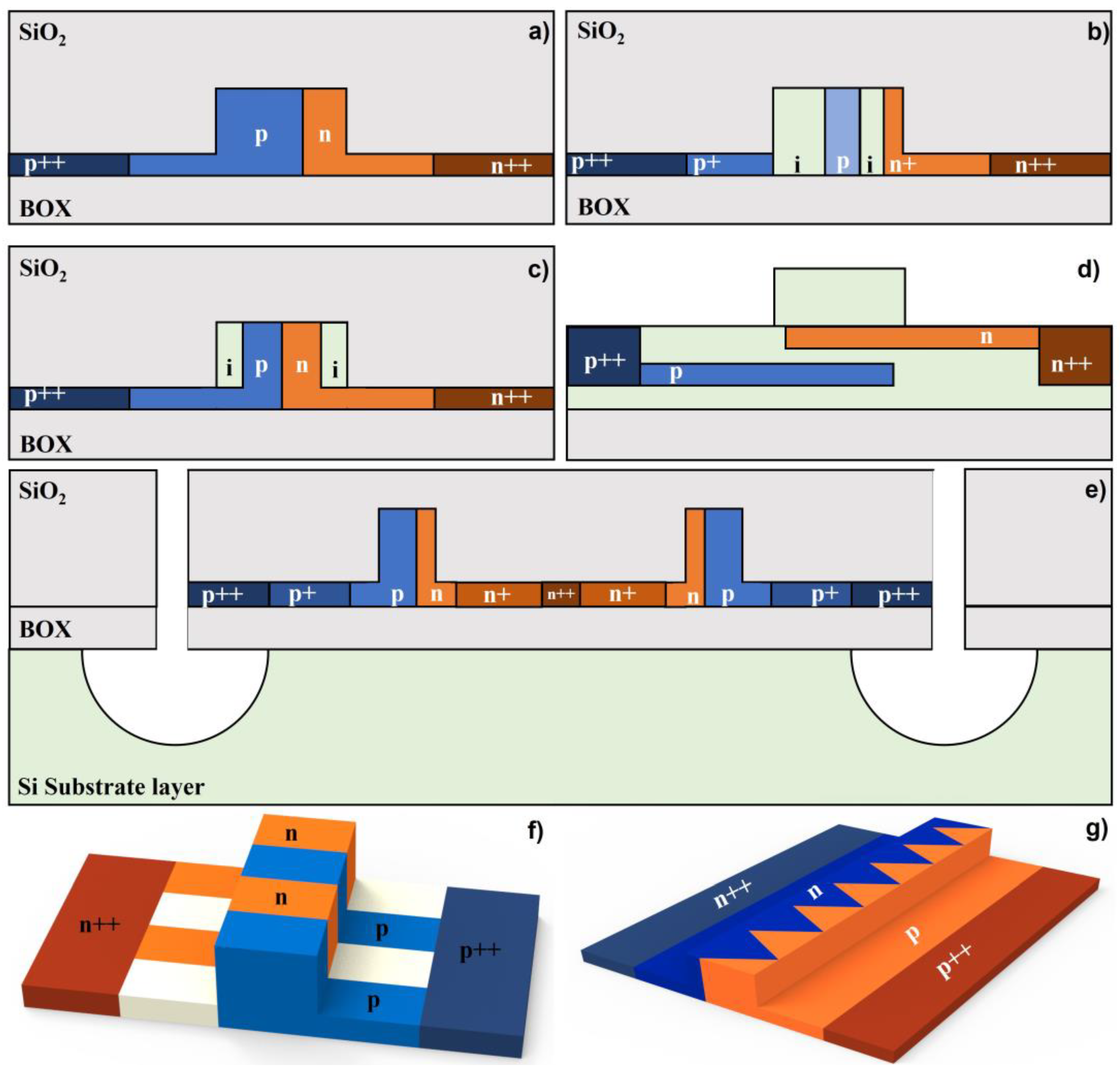
Figure 1. Various structures of free-carrier-depletion-based phase shifters. (a) Phase shifter with offset carrier doping, (b) PIPIN phase shifters, (c) phase shifter with counter doping at corners, (d) phase shifter with epitaxy fabrication, (e) phase shifters with substrate removement, (f) interleaved structure phase shifter, (g) zig-zag structure phase shifter.
2.2. Typical Work in Free-Carrier-Depletion-Based Phase Shifter
Various configurations have been proposed to balance and optimize modulation efficiency, waveguide propagation loss, and modulation speed. The waveguide propagation loss can be effectively reduced by avoiding the overlap between the waveguide mode field and the doping area. Patel et al. proposed a phase shifter with an offset doping area, which aims at reducing the optical loss and improving the modulation efficiency [40]. The target doping concentration of the p type region was 7.8e17, which is lower than that of the n type region (2.1e18). The insertion loss of the 500 μm long doping waveguide embedded in a Michelson interferometric modulator was characterized as 4.7 dB, and a 0.72 V·cm Vπ·Lπ was obtained at 1V bias voltage. Figure 1b shows a PIPIN diode phase shifter proposed by Ziebell et al. [41]. By selectively doping the waveguide (8e17 in the p+ region, 1e18 in the n+ region, and 3e17 in the p region), the transmission loss was reduced while ensuring effective modulation efficiency and modulation speed. The experimental results showed that for a 0.95 mm long phase shifter embedded in the MZI, the insertion loss was extracted as 2.5 dB, and the Vπ·Lπ was 3.5 V·cm. The modulation speed was measured as 40 GHz. Tu et al. demonstrated the carrier compensation method and set the concentration of the doped waveguide at the corner to zero [42], thereby reducing the waveguide propagation loss to 1.04 dB/mm without sacrificing the modulation efficiency (Figure 1c). The Vπ·Lπ was measured as 2.67 V·cm at 6 V bias voltage. Azadeh et al. constructed a silicon–insulator–silicon capacitive phase shifter that greatly reduced the doped waveguide area, as shown in Figure 1d [43]. Through injecting a high concentration of carriers (7e18 in the n+ region and 6e18 in the p+ region), the waveguide propagation loss was obtained as 4.2 dB/mm with the modulation efficiency of 0.74 V·cm at 2V bias voltage. The modulation speed was measured as 48 GHz.
In addition, Li et al. proposed an ultra-fast free-carrier-deletion-based phase shifter by removing the silicon substrate beneath the bus waveguide, which can reduce the useless power consumption in the substrate and thus improve the modulation bandwidth (Figure 1e) [44]. The 3 dB EO bandwidth reached up to 60 GHz at the DC bias voltage of −8 V. The waveguide propagation loss was 2.2 dB/mm and the modulation efficiency achieved was 1.4 V·cm.
By maximizing the overlap between the depletion region and the optical mode, the modulation efficiency can be improved. As shown in Figure 1f,g, interleaved junctions and zig-zag structures were proposed, which demonstrated modulation efficiency of 2.4 V·cm and 1.7 V·cm, respectively [45][46].
2.3. Discussion
Performances of some typical free-carrier-depletion-based phase shifters are summarized in Table 1. Through optimizing the concentration and distribution of free carriers in the bus waveguide, research has been carried out to balance the modulation efficiency, modulation speed, and propagation loss. Phase shifters are widely used in the data transmission and telecommunication fields, benefiting from the fast modulation speed.
Table 1. Performance summary of free-carrier-depletion-based phase shifters.
| Doping Distribution |
P Conc. (cm−3) |
N Conc. (cm−3) |
Modulation Efficiency (V·cm) |
Propagation Loss (dB/mm) |
Modulation Speed (GHz) |
Ref. |
|---|---|---|---|---|---|---|
| PN junction in the center of the waveguide |
5 × 10¹⁷ | 5 × 10¹⁷ | 1.9 (3V) | 1.2 | >20 | [47] |
| 7 × 10¹⁷ | 5 × 10¹⁷ | 3.5 (3V) | 1 | 10 | [48] | |
| 1 × 10¹⁸ | 3 × 10¹⁸ | 1.59 | 3.2 | 27 | [49] | |
| 2 × 10¹⁷ | 2 × 10¹⁷ | 1.7 (3V) | 1.2 | 12 | [50] | |
| 2 × 10¹⁸ | 2 × 10¹⁸ | 1.2 (3V) | 4.5 | 4.3 | [51] | |
| 4 × 10¹⁷ | 1.3 × 10¹⁷ | 3.2 (0–4V) | 1 | 46 | [52] | |
| Offset PN junction |
2 × 10¹⁸ | 3 × 10¹⁷ | 14.3 | - | 8 | [53] |
| 2 × 10¹⁷ | 6 × 10¹⁷ | 11 (3V) | - | 19 | [54] | |
| 2 × 10¹⁷ | 2 × 10¹⁷ | 1.8 (3V) | 1.6 | 27.8 | [55] | |
| 3 × 10¹⁷ | 1.5 × 10¹⁸ | 2.8 (4V) | 5 | 40 | [56] | |
| Interleaved waveguide |
2 × 10¹⁷ | 2 × 10¹⁷ | 1.7 (3V) | 1 | 20 | [57] |
| 2 × 10¹⁷ | 2 × 10¹⁷ | 1.4 (3V) | 1.7 | 11.8 | [58] | |
| 2 × 10¹⁸ | 2 × 10¹⁸ | 0.8 (4V) | 3.5 | 12.6 | [51] | |
| 5 × 10¹⁷ | 1 × 10¹⁸ | 2.4 | 2.1 | 20 | [45] | |
| Zig-zag waveguide |
2 × 10¹⁷ | 4 × 10¹⁷ | - | - | 23 | [46] |
| PIPIN junction | 8 × 10¹⁷/ 3 × 10¹⁷ |
1 × 10¹⁸ | 3.5 | 1 | 40 | [41] |
| Corner doping concentration | - | - | 2.67 (−6V) | - | 8.9 | [42] |
| Wrapped PN junction |
- | - | 0.52 (2V) | - | 50 | [59] |
References
- Doerr, C.R. Silicon photonic integration in telecommunications. Front. Phys. 2015, 3, 37.
- Qiang, X.; Zhou, X.; Wang, J.; Wilkes, C.M.; Loke, T.; O’Gara, S.; Kling, L.; Marshall, G.D.; Santagati, R.; Ralph, T.C. Large-scale silicon quantum photonics implementing arbitrary two-qubit processing. Nat. Photonics 2018, 12, 534–539.
- Redding, B.; Liew, S.F.; Sarma, R.; Cao, H. Compact spectrometer based on a disordered photonic chip. Nat. Photonics 2013, 7, 746–751.
- Qiao, Q.; Liu, X.; Ren, Z.; Dong, B.; Xia, J.; Sun, H.; Lee, C.; Zhou, G. MEMS-Enabled On-Chip Computational Mid-Infrared Spectrometer Using Silicon Photonics. ACS Photonics 2022, 9, 2367–2377.
- Xia, J.; Qiao, Q.; Sun, H.; Huang, Y.; Chau, F.S.; Zhou, G. Ultrasensitive nanoscale optomechanical electrometer using photonic crystal cavities. Nanophotonics 2022, 11, 1629–1642.
- Qiao, Q.; Peng, C.; Xia, J.; Lee, C.; Zhou, G. Ultra-small photonic crystal (PhC)-based test tool for gas permeability of polymers. Opt. Express 2019, 27, 35600–35608.
- Dong, B.; Zhang, Z.; Shi, Q.; Wei, J.; Ma, Y.; Xiao, Z.; Lee, C. Biometrics-protected optical communication enabled by deep learning–enhanced triboelectric/photonic synergistic interface. Sci. Adv. 2022, 8.
- Hu, T.; Dong, B.; Luo, X.; Liow, T.-Y.; Song, J.; Lee, C.; Lo, G.-Q. Silicon photonic platforms for mid-infrared applications. Photonics Res. 2017, 5, 417–430.
- Reed, G.T.; Mashanovich, G.; Gardes, F.Y.; Thomson, D. Silicon optical modulators. Nat. Photonics 2010, 4, 518–526.
- Su, Y.; Zhang, Y.; Qiu, C.; Guo, X.; Sun, L. Silicon photonic platform for passive waveguide devices: Materials, fabrication, and applications. Adv. Mater. Technol. 2020, 5, 1901153.
- Jalali, B.; Fathpour, S. Silicon photonics. J. Lightwave Technol. 2006, 24, 4600–4615.
- Soref, R. The past, present, and future of silicon photonics. IEEE J. Sel. Top. Quantum Electron. 2006, 12, 1678–1687.
- Won, R. Integrating silicon photonics. Nat. Photonics 2010, 4, 498–499.
- Rahim, A.; Hermans, A.; Wohlfeil, B.; Petousi, D.; Kuyken, B.; Van Thourhout, D.; Baets, R.G. Taking silicon photonics modulators to a higher performance level: State-of-the-art and a review of new technologies. Adv. Photonics 2021, 3, 024003.
- Witzens, J. High-speed silicon photonics modulators. Proc. IEEE 2018, 106, 2158–2182.
- Qiao, Q.; Sun, H.; Liu, X.; Dong, B.; Xia, J.; Lee, C.; Zhou, G. Suspended silicon waveguide with sub-wavelength grating cladding for optical mems in mid-infrared. Micromachines 2021, 12, 1311.
- Qiao, Q.; Yazici, M.S.; Dong, B.; Liu, X.; Lee, C.; Zhou, G. Multifunctional mid-infrared photonic switch using a MEMS-based tunable waveguide coupler. Opt. Lett. 2020, 45, 5620–5623.
- Rickman, A. The commercialization of silicon photonics. Nat. Photonics 2014, 8, 579–582.
- Selvaraja, S.K.; De Heyn, P.; Winroth, G.; Ong, P.; Lepage, G.; Cailler, C.; Rigny, A.; Bourdelle, K.K.; Bogaerts, W.; van Thourhout, D. Highly uniform and low-loss passive silicon photonics devices using a 300mm CMOS platform. In Proceedings of the Optical Fiber Communication Conference, San Francisco, CA, USA, 9–13 March 2014.
- Carroll, L.; Lee, J.-S.; Scarcella, C.; Gradkowski, K.; Duperron, M.; Lu, H.; Zhao, Y.; Eason, C.; Morrissey, P.; Rensing, M. Photonic packaging: Transforming silicon photonic integrated circuits into photonic devices. Appl. Sci. 2016, 6, 426.
- Jo, G.; Edinger, P.; Bleiker, S.J.; Wang, X.; Takabayashi, A.Y.; Sattari, H.; Quack, N.; Jezzini, M.; Lee, J.S.; Verheyen, P. Wafer-level hermetically sealed silicon photonic MEMS. Photonics Res. 2022, 10, A14–A21.
- Zimmermann, L.; Preve, G.B.; Tekin, T.; Rosin, T.; Landles, K. Packaging and assembly for integrated photonics—A review of the ePIXpack photonics packaging platform. IEEE J. Sel. Top. Quantum Electron. 2010, 17, 645–651.
- Choi, C.; Kim, H.; Kang, J.-H.; Song, M.-K.; Yeon, H.; Chang, C.S.; Suh, J.M.; Shin, J.; Lu, K.; Park, B.-I. Reconfigurable heterogeneous integration using stackable chips with embedded artificial intelligence. Nat. Electron. 2022, 5, 386–393.
- Errando-Herranz, C.; Takabayashi, A.Y.; Edinger, P.; Sattari, H.; Gylfason, K.B.; Quack, N. MEMS for Photonic Integrated Circuits. IEEE J. Sel. Top. Quantum Electron. 2020, 26, 8200916.
- Cheng, Z.; Ríos, C.; Pernice, W.H.; Wright, C.D.; Bhaskaran, H. On-chip photonic synapse. Sci. Adv. 2017, 3, e1700160.
- Shastri, B.J.; Tait, A.N.; Ferreira de Lima, T.; Pernice, W.H.; Bhaskaran, H.; Wright, C.D.; Prucnal, P.R. Photonics for artificial intelligence and neuromorphic computing. Nat. Photonics 2021, 15, 102–114.
- Hutchison, D.N.; Sun, J.; Doylend, J.K.; Kumar, R.; Heck, J.; Kim, W.; Phare, C.T.; Feshali, A.; Rong, H. High-resolution aliasing-free optical beam steering. Optica 2016, 3, 887–890.
- Kwong, D.; Hosseini, A.; Covey, J.; Zhang, Y.; Xu, X.; Subbaraman, H.; Chen, R.T. On-chip silicon optical phased array for two-dimensional beam steering. Opt. Lett. 2014, 39, 941–944.
- Sun, J.; Timurdogan, E.; Yaacobi, A.; Hosseini, E.S.; Watts, M.R. Large-scale nanophotonic phased array. Nature 2013, 493, 195–199.
- Heck, M.J. Highly integrated optical phased arrays: Photonic integrated circuits for optical beam shaping and beam steering. Nanophotonics 2017, 6, 93–107.
- Poulton, C.V.; Byrd, M.J.; Russo, P.; Timurdogan, E.; Khandaker, M.; Vermeulen, D.; Watts, M.R. Long-range LiDAR and free-space data communication with high-performance optical phased arrays. IEEE J. Sel. Top. Quantum Electron. 2019, 25, 7700108.
- Zhang, X.; Kwon, K.; Henriksson, J.; Luo, J.; Wu, M.C. A large-scale microelectromechanical-systems-based silicon photonics LiDAR. Nature 2022, 603, 253–258.
- Ryckeboer, E.; Nie, X.; Subramanian, A.Z.; Martens, D.; Bienstman, P.; Clemmen, S.; Severi, S.; Jansen, R.; Roelkens, G.; Baets, R. CMOS-compatible silicon nitride spectrometers for lab-on-a-chip spectral sensing. In Proceedings of the Silicon Photonics and Photonic Integrated Circuits V, Brussels, Belgium, 5–7 April 2016; pp. 274–282.
- Zhang, L.; Zhang, M.; Chen, T.; Liu, D.; Hong, S.; Dai, D. Ultrahigh-resolution on-chip spectrometer with silicon photonic resonators. Opto-Electron. Adv. 2022, 5, 210100.
- Zheng, S.N.; Zou, J.; Cai, H.; Song, J.; Chin, L.; Liu, P.; Lin, Z.; Kwong, D.; Liu, A. Microring resonator-assisted Fourier transform spectrometer with enhanced resolution and large bandwidth in single chip solution. Nat. Commun. 2019, 10, 2349.
- Feldmann, J.; Youngblood, N.; Karpov, M.; Gehring, H.; Li, X.; Stappers, M.; Le Gallo, M.; Fu, X.; Lukashchuk, A.; Raja, A.S. Parallel convolutional processing using an integrated photonic tensor core. Nature 2021, 589, 52–58.
- Xu, X.; Tan, M.; Corcoran, B.; Wu, J.; Boes, A.; Nguyen, T.G.; Chu, S.T.; Little, B.E.; Hicks, D.G.; Morandotti, R. 11 TOPS photonic convolutional accelerator for optical neural networks. Nature 2021, 589, 44–51.
- Reed, G.T.; Mashanovich, G.Z.; Gardes, F.Y.; Nedeljkovic, M.; Hu, Y.; Thomson, D.J.; Li, K.; Wilson, P.R.; Chen, S.-W.; Hsu, S.S. Recent breakthroughs in carrier depletion based silicon optical modulators. Nanophotonics 2014, 3, 229–245.
- Lin, H.; Luo, Z.; Gu, T.; Kimerling, L.C.; Wada, K.; Agarwal, A.; Hu, J. Mid-infrared integrated photonics on silicon: A perspective. Nanophotonics 2018, 7, 393–420.
- Patel, D.; Veerasubramanian, V.; Ghosh, S.; Samani, A.; Zhong, Q.; Plant, D.V. High-speed compact silicon photonic Michelson interferometric modulator. Opt. Express 2014, 22, 26788–26802.
- Ziebell, M.; Marris-Morini, D.; Rasigade, G.; Fédéli, J.-M.; Crozat, P.; Cassan, E.; Bouville, D.; Vivien, L. 40 Gbit/s low-loss silicon optical modulator based on a pipin diode. Opt. Express 2012, 20, 10591–10596.
- Tu, X.; Liow, T.-Y.; Song, J.; Luo, X.; Fang, Q.; Yu, M.; Lo, G.-Q. 50-Gb/s silicon optical modulator with traveling-wave electrodes. Opt. Express 2013, 21, 12776–12782.
- Azadeh, S.S.; Merget, F.; Romero-García, S.; Moscoso-Mártir, A.; von den Driesch, N.; Müller, J.; Mantl, S.; Buca, D.; Witzens, J. Low V π Silicon photonics modulators with highly linear epitaxially grown phase shifters. Opt. Express 2015, 23, 23526–23550.
- Li, M.; Wang, L.; Li, X.; Xiao, X.; Yu, S. Silicon intensity Mach–Zehnder modulator for single lane 100 Gb/s applications. Photonics Res. 2018, 6, 109–116.
- Marris-Morini, D.; Baudot, C.; Fédéli, J.; Rasigade, G.; Vulliet, N.; Souhaité, A.; Ziebell, M.; Rivallin, P.; Olivier, S.; Crozat, P. Low loss 40 Gbit/s silicon modulator based on interleaved junctions and fabricated on 300 mm SOI wafers. Opt. Express 2013, 21, 22471–22475.
- Xiao, X.; Li, X.; Xu, H.; Li, Z.; Chu, T.; Yu, J.; Yu, Y. High-speed silicon microring modulator based on zigzag PN junction. In Proceedings of the IEEE Photonics Conference 2012, Burlingame, CA, USA, 23–27 September 2012; pp. 256–257.
- Dong, P.; Chen, L.; Chen, Y.-k. High-speed low-voltage single-drive push-pull silicon Mach-Zehnder modulators. Opt. Express 2012, 20, 6163–6169.
- Baehr-Jones, T.; Ding, R.; Liu, Y.; Ayazi, A.; Pinguet, T.; Harris, N.C.; Streshinsky, M.; Lee, P.; Zhang, Y.; Lim, A.E.-J. Ultralow drive voltage silicon traveling-wave modulator. Opt. Express 2012, 20, 12014–12020.
- Kim, G.; Park, J.W.; Kim, I.G.; Kim, S.; Kim, S.; Lee, J.M.; Park, G.S.; Joo, J.; Jang, K.-S.; Oh, J.H. Low-voltage high-performance silicon photonic devices and photonic integrated circuits operating up to 30 Gb/s. Opt. Express 2011, 19, 26936–26947.
- Li, X.; Xiao, X.; Xu, H.; Li, Z.; Chu, T.; Yu, J.; Yu, Y. Highly efficient silicon Michelson interferometer modulators. IEEE Photonics Technol. Lett. 2013, 25, 407–409.
- Yu, H.; Pantouvaki, M.; Van Campenhout, J.; Korn, D.; Komorowska, K.; Dumon, P.; Li, Y.; Verheyen, P.; Absil, P.; Alloatti, L. Performance tradeoff between lateral and interdigitated doping patterns for high speed carrier-depletion based silicon modulators. Opt. Express 2012, 20, 12926–12938.
- Merget, F.; Azadeh, S.S.; Mueller, J.; Shen, B.; Nezhad, M.P.; Hauck, J.; Witzens, J. Silicon photonics plasma-modulators with advanced transmission line design. Opt. Express 2013, 21, 19593–19607.
- You, J.-B.; Park, M.; Park, J.-W.; Kim, G. 12.5 Gbps optical modulation of silicon racetrack resonator based on carrier-depletion in asymmetric pn diode. Opt. Express 2008, 16, 18340–18344.
- Gardes, F.; Brimont, A.; Sanchis, P.; Rasigade, G.; Marris-Morini, D.; O’Faolain, L.; Dong, F.; Fedeli, J.; Dumon, P.; Vivien, L. High-speed modulation of a compact silicon ring resonator based on a reverse-biased pn diode. Opt. Express 2009, 17, 21986–21991.
- Xiao, X.; Xu, H.; Li, X.; Li, Z.; Chu, T.; Yu, Y.; Yu, J. High-speed, low-loss silicon Mach–Zehnder modulators with doping optimization. Opt. Express 2013, 21, 4116–4125.
- Thomson, D.J.; Gardes, F.Y.; Fedeli, J.-M.; Zlatanovic, S.; Hu, Y.; Kuo, B.P.P.; Myslivets, E.; Alic, N.; Radic, S.; Mashanovich, G.Z. 50-Gb/s silicon optical modulator. IEEE Photonics Technol. Lett. 2011, 24, 234–236.
- Xu, H.; Xiao, X.; Li, X.; Hu, Y.; Li, Z.; Chu, T.; Yu, Y.; Yu, J. High speed silicon Mach-Zehnder modulator based on interleaved PN junctions. Opt. Express 2012, 20, 15093–15099.
- Xiao, X.; Xu, H.; Li, X.; Hu, Y.; Xiong, K.; Li, Z.; Chu, T.; Yu, Y.; Yu, J. 25 Gbit/s silicon microring modulator based on misalignment-tolerant interleaved PN junctions. Opt. Express 2012, 20, 2507–2515.
- Sun, J.; Kumar, R.; Sakib, M.; Driscoll, J.B.; Jayatilleka, H.; Rong, H. A 128 Gb/s PAM4 silicon microring modulator with integrated thermo-optic resonance tuning. J. Lightwave Technol. 2018, 37, 110–115.
More
Information
Subjects:
Engineering, Electrical & Electronic
Contributors
MDPI registered users' name will be linked to their SciProfiles pages. To register with us, please refer to https://encyclopedia.pub/register
:
View Times:
1.7K
Revisions:
3 times
(View History)
Update Date:
28 Sep 2022
Table of Contents


Notice
You are not a member of the advisory board for this topic. If you want to update advisory board member profile, please contact office@encyclopedia.pub.
OK
Confirm
Only members of the Encyclopedia advisory board for this topic are allowed to note entries. Would you like to become an advisory board member of the Encyclopedia?
Yes
No
${ textCharacter }/${ maxCharacter }
Submit
Cancel
Back
Comments
${ item }
|
${ item.createdUser.fullName }
${ item.createdAt }
${ item.vote }
${ item.reply }
Delete
${ reply.createdUser.fullName }
${ reply.createdAt }
${ reply.vote }
Delete
There is no reply to this comment~
${ item.replyTextCharacter }/${ item.replyMaxCharacter }
Submit
Cancel
More
No more~
There is no comment~
${ textCharacter }/${ maxCharacter }
Submit
Cancel
${ selectedItem.replyTextCharacter }/${ selectedItem.replyMaxCharacter }
Submit
Cancel
Confirm
Are you sure to Delete?
Yes
No