Your browser does not fully support modern features. Please upgrade for a smoother experience.
Please note this is a comparison between Version 1 by Guangya Zhou and Version 3 by Camila Xu.
Free-carrier-dispersion-based phase shifters are favored in the field of telecommunications and data centers due to their high modulation speed and low power consumption. Based on the working mechanism, free-carrier-dispersion-based phase shifters fall into three categories: carrier injection, carrier depletion, and carrier accumulation.
- silicon photonics
- phase shifters
- MEMS
- thermo-optics
- Free carrier depletion
1. Introduction
The past few decades have witnessed a huge growth in silicon photonics. Photonic integrated circuits (PICs) have been widely used and studied in areas such as telecommunications, lab-on-a-chip sensing, and quantum computing [1][2][3][4][5][6][7][1,2,3,4,5,6,7]. Benefitting from the broadband optical transparency (from 1.3 μm to 8 μm), high refractive index (n = 3.4757 at λ = 1550 nm, room temperature), and compatible manufacturing process with matured complementary metal–oxide semiconductor (CMOS) technologies [8][9][10][8,9,10], the silicon-on-insulator (SOI) substrate has become one of the most important platforms for on-chip PICs [11][12][13][11,12,13]. To meet the rapidly increasing demand for data communication, optical path routing, and optical signal modulation, passive and active optical components based on the SOI platform have been extensively studied in the past few decades [8][9][10][14][15][16][17][8,9,10,14,15,16,17]. Furthermore, the commercialization of silicon photonics has begun to take shape [18]. Some matured and advanced commercial foundries, such as the Advanced Micro Foundry (AMF) from Singapore, the American Institute for Manufacturing Integrated Photonics (AIM) from the United States, and the Interuniversity Microelectronics Centre (IMEC) from Belgium, have made great efforts and built promising PIC component libraries, including strip and rib waveguide, power splitter, grating coupler, waveguide crossing, directional coupler, micro-ring resonator, thermal-optical phase shifter, and so on. With intensive efforts, the propagation loss of silicon wire waveguide has been reduced to below 1.0 dB/cm by researchers, which paves the way to build large-scale PIC applications [19]. Moreover, packaging technology has been extensively explored [20][21][22][23][20,21,22,23], which leads to a high-level chip-scale integration including on-chip components such as photodetector (PD), modulator, laser source, and fiber-to-chip coupler.
With the development of dense PICs, effective and high-performance on-chip active components are urgently needed to realize complex on-chip functions. Phase shifters are one of the most important components in building PICs. A building block that offers two inputs and two outputs capable of power tuning and phase shifting can be considered a fundamental unit in large-scale PICs [24]. The phase shifter here refers to modulating the phase of the transmission wave only without changing the amplitude, where the power tuning function can be obtained by forming the interferometer based on phase shifters. Using enough amounts of such building blocks, an arbitrary linear optical system can be built. Using well-integrated phase shifters, researchers have reported various applications such as neuromorphic computing systems [25][26][25,26], optical phased arrays [27][28][29][30][27,28,29,30], light detection and ranging (LiDAR) systems [31][32][31,32], on-chip spectrometers [33][34][35][33,34,35], photonic accelerators [26][36][37][26,36,37], and so on.
2. Free-Carrier-Depletion-Based Phase Shifter
Free-carrier-dispersion-based phase shifters are favored in the field of telecommunications and data centers due to their high modulation speed and low power consumption. Based on the working mechanism, free-carrier-dispersion-based phase shifters fall into three categories: carrier injection, carrier depletion, and carrier accumulation. In this section, rwesearchers introduce the free-carrier-depletion-based phase shifter only. Some outstanding reviews of free-carrier-based phase shifters can be found in [9][14][15][38][9,14,15,82].
2.1. Modulation Principle
Free-carrier-depletion-based phase shifters usually modulate the phase of transmission wave by changing the carrier concentration in the core material of the bus waveguide. The refractive index changes (Δn) and carrier absorption (Δα) caused by free-carrier concentration change can be described by the Drude model [39][83]:
and
where e refers to the elementary charge, λ is the laser wavelength, c is the light speed, ε0 denotes the vacuum permittivity, n represents the unperturbed refractive index of the material, ΔN is the charge carrier density, m* refers to the carrier effective mass, and the subscripts e and h indicate quantities related to electrons and holes, respectively.
Some free-carrier-depletion-based phase shifter structures are shown in Figure 19. Rib waveguide is usually used, benefitting from a pair of thin film slabs. The cross-section is divided into an enhanced doping concentration region (p++/n++ region), a doping concentration region (p+/n+ region), and an intrinsic region (i region). Doping area distributions and doping concentrations are the most important parameters, which affect the modulation efficiency (Vπ·Lπ) and waveguide propagation loss (α). Electro-optic bandwidth is regarded to represent the modulation speed.
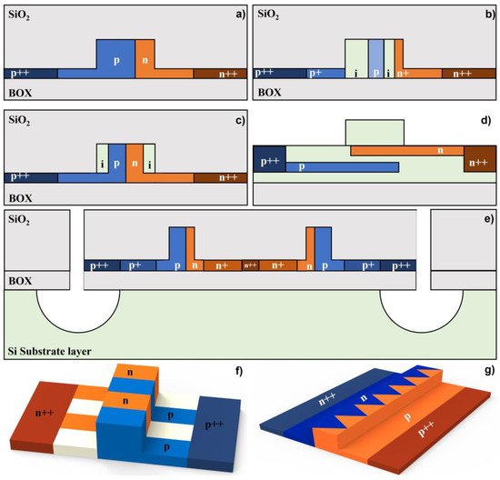
Figure 19. Various structures of free-carrier-depletion-based phase shifters. (a) Phase shifter with offset carrier doping, (b) PIPIN phase shifters, (c) phase shifter with counter doping at corners, (d) phase shifter with epitaxy fabrication, (e) phase shifters with substrate removement, (f) interleaved structure phase shifter, (g) zig-zag structure phase shifter.
2.2. Typical Work in Free-Carrier-Depletion-Based Phase Shifter
Various configurations have been proposed to balance and optimize modulation efficiency, waveguide propagation loss, and modulation speed. The waveguide propagation loss can be effectively reduced by avoiding the overlap between the waveguide mode field and the doping area. Patel et al. proposed a phase shifter with an offset doping area, which aims at reducing the optical loss and improving the modulation efficiency [40][84]. The target doping concentration of the p type region was 7.8e17, which is lower than that of the n type region (2.1e18). The insertion loss of the 500 μm long doping waveguide embedded in a Michelson interferometric modulator was characterized as 4.7 dB, and a 0.72 V·cm Vπ·Lπ was obtained at 1V bias voltage. Figure 19b shows a PIPIN diode phase shifter proposed by Ziebell et al. [41][85]. By selectively doping the waveguide (8e17 in the p+ region, 1e18 in the n+ region, and 3e17 in the p region), the transmission loss was reduced while ensuring effective modulation efficiency and modulation speed. The experimental results showed that for a 0.95 mm long phase shifter embedded in the MZI, the insertion loss was extracted as 2.5 dB, and the Vπ·Lπ was 3.5 V·cm. The modulation speed was measured as 40 GHz. Tu et al. demonstrated the carrier compensation method and set the concentration of the doped waveguide at the corner to zero [42][86], thereby reducing the waveguide propagation loss to 1.04 dB/mm without sacrificing the modulation efficiency (Figure 19c). The Vπ·Lπ was measured as 2.67 V·cm at 6 V bias voltage. Azadeh et al. constructed a silicon–insulator–silicon capacitive phase shifter that greatly reduced the doped waveguide area, as shown in Figure 19d [43][87]. Through injecting a high concentration of carriers (7e18 in the n+ region and 6e18 in the p+ region), the waveguide propagation loss was obtained as 4.2 dB/mm with the modulation efficiency of 0.74 V·cm at 2V bias voltage. The modulation speed was measured as 48 GHz. In addition, Li et al. proposed an ultra-fast free-carrier-deletion-based phase shifter by removing the silicon substrate beneath the bus waveguide, which can reduce the useless power consumption in the substrate and thus improve the modulation bandwidth (Figure 19e) [44][88]. The 3 dB EO bandwidth reached up to 60 GHz at the DC bias voltage of −8 V. The waveguide propagation loss was 2.2 dB/mm and the modulation efficiency achieved was 1.4 V·cm. By maximizing the overlap between the depletion region and the optical mode, the modulation efficiency can be improved. As shown in Figure 19f,g, interleaved junctions and zig-zag structures were proposed, which demonstrated modulation efficiency of 2.4 V·cm and 1.7 V·cm, respectively [45][46][89,90].2.3. Discussion
Performances of some typical free-carrier-depletion-based phase shifters are summarized in Table 13. Through optimizing the concentration and distribution of free carriers in the bus waveguide, research has been carried out to balance the modulation efficiency, modulation speed, and propagation loss. Phase shifters are widely used in the data transmission and telecommunication fields, benefiting from the fast modulation speed.Table 13.
Performance summary of free-carrier-depletion-based phase shifters.
| Doping Distribution |
P Conc. (cm−3) |
N Conc. (cm−3) |
Modulation Efficiency (V·cm) |
Propagation Loss (dB/mm) |
Modulation Speed (GHz) |
Ref. |
|---|---|---|---|---|---|---|
| PN junction in the center of the waveguide |
5 × 10¹⁷ | 5 × 10¹⁷ | 1.9 (3V) | 1.2 | >20 | [47][91] |
| 7 × 10¹⁷ | 5 × 10¹⁷ | 3.5 (3V) | 1 | 10 | [48][92] | |
| 1 × 10¹⁸ | 3 × 10¹⁸ | 1.59 | 3.2 | 27 | [49][93] | |
| 2 × 10¹⁷ | 2 × 10¹⁷ | 1.7 (3V) | 1.2 | 12 | [50][94] | |
| 2 × 10¹⁸ | 2 × 10¹⁸ | 1.2 (3V) | 4.5 | 4.3 | [51][95] | |
| 4 × 10¹⁷ | 1.3 × 10¹⁷ | 3.2 (0–4V) | 1 | 46 | [52][96] | |
| Offset PN junction |
2 × 10¹⁸ | 3 × 10¹⁷ | 14.3 | - | 8 | [53][97] |
| 2 × 10¹⁷ | 6 × 10¹⁷ | 11 (3V) | - | 19 | [54][98] | |
| 2 × 10¹⁷ | 2 × 10¹⁷ | 1.8 (3V) | 1.6 | 27.8 | [55][99] | |
| 3 × 10¹⁷ | 1.5 × 10¹⁸ | 2.8 (4V) | 5 | 40 | [56][100] | |
| Interleaved waveguide |
2 × 10¹⁷ | 2 × 10¹⁷ | 1.7 (3V) | 1 | 20 | [57][101] |
| 2 × 10¹⁷ | 2 × 10¹⁷ | 1.4 (3V) | 1.7 | 11.8 | [58][102] | |
| 2 × 10¹⁸ | 2 × 10¹⁸ | 0.8 (4V) | 3.5 | 12.6 | [51][95] | |
| 5 × 10¹⁷ | 1 × 10¹⁸ | 2.4 | 2.1 | 20 | [45][89] | |
| Zig-zag waveguide |
2 × 10¹⁷ | 4 × 10¹⁷ | - | - | 23 | [46][90] |
| PIPIN junction | 8 × 10¹⁷/ 3 × 10¹⁷ |
1 × 10¹⁸ | 3.5 | 1 | 40 | [41][85] |
| Corner doping concentration | - | - | 2.67 (−6V) | - | 8.9 | [42][86] |
| Wrapped PN junction |
- | - | 0.52 (2V) | - | 50 | [59][103] |