 +1 credit
| Version | Summary | Created by | Modification | Content Size | Created at | Operation |
|---|---|---|---|---|---|---|
| 1 | Amine El Moutaouakil | + 3248 word(s) | 3248 | 2021-05-10 12:41:34 | | | |
| 2 | Peter Tang | Meta information modification | 3248 | 2021-05-14 04:22:41 | | |
Video Upload Options
Molybdenum disulfide (MoS2) is one of the compounds discussed nowadays due to its outstanding properties that allowed its usage in different applications. Its band gap and its distinctive structure make it a promising material to substitute graphene and other semiconductor devices. It has different applications in electronics especially sensors like optical sensors, biosensors, electrochemical biosensors that play an important role in the detection of various diseases’ like cancer and Alzheimer. It has a wide range of energy applications in batteries, solar cells, microwave, and Terahertz applications. It is a promising material on a nanoscale level, with favorable characteristics in spintronics and magnetoresistance.
1. Introduction
Molybdenum disulfide (MoS2) is an inorganic compound of the transition metal dichalcogenides (TMDs) series, that has one atom of Molybdenum and two atoms of Sulfur. Dichalcogenides are chemical compounds consisting of a transition metal, like Molybdenum, and a chalcogen (element of group 16 in the periodic table) like sulfur (S) [1]. The physical, chemical, and electronic properties of this compound grabbed the attention of many researchers and were found promising materials to substitute previously used semiconductor and/or graphene devices. As the world is moving towards miniaturization, researchers were searching for a material to substitute semiconductor devices that seemed to reach an end when entering the nanoscale era [2]. While semiconductors devices based on Silicon were facing quantum and tunneling effects on a nanoscale level, MoS2 showed favorable and promising electronic and quantum characteristics when going from bulk to two-dimensional (2D) structure [3].
MoS2 seems to solve many problems facing previous devices [4][5][6][7][8], it has a large band gap (~1.8 eV) which changes from an indirect gap to a direct one in thin structures. This would permit downscaling electronic devices, rather than graphene which nearly has a zero-band gap [9][10]. It does not have surface dangling bonds and has high mobility even with high-κ dielectric materials. It is ideal for thin-film transistors, and its fabrication is simple which means large production yield and low cost [11][12]. The covalent bonds between Molybdenum and Sulfur and the Van der Waals bonds between its layers make it optimal for gas sensing. One of the major problems with Silicon devices was that related to the metal-semiconductor interface [13]. MoS2 has less contact resistance and high performance. In other words, MoS2 has potency to be used in 1 nm gate transistors with excellent on/off switching characteristics and high efficiency [14].
Silicon transistors fabrication faced some problems on the bulk scale that were overcome by new structures such as multi-gate transistors, but when going down to the nanoscale, the fabrication process seems to reach an end. The metal interconnection lines between transistors have high density and are very narrow, which cause an increase in resistance and capacitance between interconnect lines and high delays. Tunneling problems are more obvious with thin gate oxides and when trying to substitute silicon dioxide with other high-κ dielectric materials, more serious problems like thermal instability, channel mobility degradation, incompatibility with the interface aroused. All these issues lead to performance degradation, and high cost with a small yield. The high lithography resolution needed for small half-pitch (HP) ~20 nm, is not easily achieved and needs high techniques and tools in lithography [15][16]. On the other side, MoS2 showed easier and simpler ways of synthesis and device fabrication [17]. It is easily prepared by spreading the molybdenum metal and sulfur and letting them self-propagate under a high temperature [18]. A MoS2 field effect transistor was fabricated in [19] by immersing it in an electrolyte, the device showed lower contact resistance and a better gate control.
MoS2 has a wide range of applications in different fields. Like Silicon and graphene, it has applications in biosensing, and optical sensors but the most important ones are those related to bio-applications like DNA, cancer, and Corona Virus detection [20][21][22][23]. While Silicon and graphene were still under study in their compatibility with human bodies, a study, in [24], showed that MoS2 may be very effective in curing cancer and Alzheimer’s disease. It also showed that the compound has no biological interaction which makes it safe for injection in human bodies. Another study in [25] proposed a biocompatible device made of MoS2 to restore some visual malfunctioning. The compound applications are not restricted to electronics, but it can serve as a lubricant [26] and is used in hydrogen evolution reactions. It is a suitable material for batteries’ electrodes [27]. Indeed, MoS2 properties and structure made it promising for several electronic, sensing, microwave, and terahertz applications.
2. Structure and Properties
MoS2 structures differ from 3D, 2D, one-dimensional (1D), or dot structures. Its characteristics and applications also change from one dimension to another, they can be semiconducting, metallic or superconducting. It exists in several layers and shapes. Its bulk (3D) structure can be tri-agonal (T), hexagonal (H), and Rhombohedral (R), where 2H MoS2 means 2-layer hexagonal shape MoS2. The three main structures are 1T, 2H and 3R, where the 1T phase coordinates in an octahedral structure, 2H and 3R in a trigonal prismatic structure [28][29] as shown in Figure 1. The lattice constants for each structure are shown in Table 1 [30]. The 1T structure is known to be metallic while the other two are semiconducting. The monolayer of hexagonal MoS2 is also semiconducting. Both 2H and 3R are used as dry lubricants. Due to the nonlinear optical properties of 3R phase it is used in nonlinear optical mass sensing in quantum measurements and biomedicine [31]. As an example, for gas sensors, the different phase materials of MoS2 can be interesting in obtaining high sensitivity and rapid desorption [32].
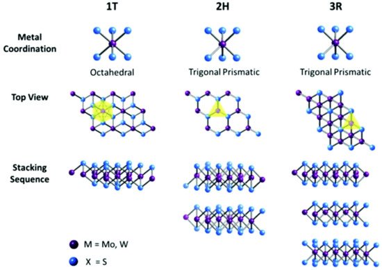
Figure 1. Different coordination and stacking sequences of the three MoS2 structures 1T, 2H and 3R. Reproduced from [29]. Published by The Royal Society of Chemistry.
Table 1. Comparison between different MoS2 structures.
|
1T |
2H |
3R |
|
|---|---|---|---|
|
Structure Coordination |
Octahedral |
Trigonal Prismatic |
Trigonal Prismatic |
|
Lattice parameters |
a = 5.60 A, c = 5.99 A and an edge sharing octahedral [30] |
a = 3.15 A, c = 12.30 A [30] |
a = 3.17 Å, c = 18.38 A [30] |
|
property |
paramagnetic and metallic |
Semiconducting |
|
|
Electrical conductivity |
105 times higher than 2H phase |
Low (~0.1 S/m) |
|
|
Absorption peaks |
No peaks at 604 nm and 667 nm |
Showed peaks at 604 nm and 667 nm |
|
|
Common applications |
Intercalation in chemistry |
Dry lubricants |
Dry lubricants and non-linear optical devices |
1H MoS2 is the most stable configuration and it is formed of one layer of Sulfur and one layer of Mo where S-Mo-S are attached through strong covalent bond like a sandwich, with a thickness of approximately 0.65 nm [33], The sandwiched S-Mo-S layers are attached through weak Wander Val forces [34]. The conductivity of nano MoS2 depends on the temperature and thickness of the flakes, where conductivity increases with the temperature increase and decreases with increasing the thickness till it reaches the bulk structure [35]. The binding energies and photoluminescence properties are summarized in Table 2 [36].
Table 2. Comparison between Bulk and monolayer MoS2.
|
Bulk |
Monolayer |
|
|---|---|---|
|
Bandgap |
Indirect (~1.2 eV) |
Direct (1.8 eV) |
|
Binding energy |
0.1 eV |
1.1 eV |
|
Photoluminescence intensities |
between 10−5 and 10−6 |
104 times higher than that of bulk, up to and up to 4 × 10⁻³ |
MoS2 exists in different 2D structure like nanosheets, and nanoribbons or 1D structures as nanowires and nanotubes, or 0D structure as quantum dots and nanoplatelets. The thickness of 2D nanoribbons was found to be of 1 to 3 layers of MoS2, while the thickness of 1D nanowires (NW) can have lengths from 14 to 30 nm and a width of 0.6 nm approximately [37]. The structure of 1D nanoplatelets and their properties were investigated in [38]. The nanoplatelets are 12–30 nm with one-unit cell width. They have very high catalytic activity for hydrodesulphurization. The quantum dots range from 2 to 10 nm in size. They have higher band gap than nanosheets, and stronger bonds between Mo atoms than monolayers. The change in band gap of MoS2 from one dimension to another, changes the photoluminescence characteristics and thus has different optical properties according to its dimension. Additionally, monolayers or other low dimension forms are also easy to be implemented in optical nanostructures to enhance the photoluminescence intensities and emission rates through light-matter interactions [39][40][41]. This is a strong motivation for MoS2 to be included in optical applications [42].
3. Synthesis
There are different techniques used to obtain material layers Figure 2, and each one of them results in different quantities, shapes, and sizes. Mainly the approaches used in synthesizing TMDs nanostructures, are the top-down approach and the bottom-up approach [43][44]. The first approach depends on etching crystal planes from a substrate that has the crystals laid over it, while in the second approach, the crystals are stacked over the substrate. Exfoliation is one of the top-bottom techniques for obtaining MoS2 layers. The weak Van der Waal forces between layers of TMDs paved the way in front of different exfoliation synthesizing techniques [45]. Mechanical exfoliation is done using a sticky tape which is rubbed out and shifted on a substrate having MoS2 flakes over it. The method gives low yield and is good for lab use. Exfoliation can also be done in the liquid phase by adding a chemical compound and stirring, bubbling, or grinding. This method is simple and cheap but has low quality. The low yield in liquid exfoliation was avoided using carbon aerogel composites in [46]. The synthesizing is fast and completed in 30 minutes. It also avoids pyrophoric materials that are typically used in liquid exfoliation and increases the electrical conductivity and porosity of MoS2. Sonication is one of the techniques that showed simple synthesis when used with liquid exfoliation [47][48]. It disposes of the use of hazardous materials used in liquid exfoliation. It is based on ultrasonic waves emitted from a probe in shape of bubbles that peels MoS2 layers when they burst. The challenge in using sonication assisted techniques is that it produces relatively small area MoS2 nanosheets that limits its use in practical applications. Generally Top down techniques are said to have low controllability, and scalability and high cost [43]. The yield is increased to >90% when using ultrasound sonication with supercritical carbon in [49] with an intercalating solvent N-methyl-2-pyrrolidone (NMP). The method is fast, simple and scalable. Sputtering is used to prepare layers of MoS2 to be used as lubricants, the layers have a low friction coefficient, but these frictional properties can be changed under humidity, especially for thin films of MoS2.
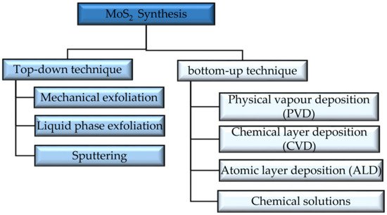
Figure 2. Different MoS2 synthesis techniques [27].
Physical layer deposition (PVD) is one of the bottom-up techniques that includes ion implantation like molecular beam epitaxy (MBE) [50]. The method can be applied only to thin layers of MoS2 and the resulting grain sizes are variable [51]. Chemical vapor deposition (CVD) is applied to thin and thick layers, where Mo is laid over a substrate and Sulfur vapor passes over it. This method has good quality, but low yield. The atomic layer deposition (ALD) method is used to fabricate thick and thin films. The method is considered efficient and the layers have fewer impurities that can be used in different applications, including electronics and sensors. MoS2 layers can be synthesized with the help of chemical solutions, using hydrothermal and solvothermal reactions wherein both cases Mo and S react in an aqueous solution above the boiling point and in a nonaqueous solution at high temperature, respectively. The size and shape of the layers can be controlled where we can get powder and thin films of MoS2 by this method. It is considered cheap and scalable [52].
In [53], MoS2 is synthesized using a liquid organic precursor on an insulating substrate using CVD. The used method is more reproducible and is used to obtain larger areas of MoS2 layers than those obtained with methods using powder Molybdenum oxide and sulfur powder. Another method in [54] used thermal evaporation and ALD, where it used metalloporphyrin as a promoter layer. The method allowed to manipulate the carrier density and conductivity of MoS2 according to the thickness of the metalloporphyrin layer used. It is used to produce MoS2 nanosheets on a large scale. In [18], MoS2 is synthesized using self-propagating, under high temperature, where Mo nanopowders and elementary Sulfur are used. The mixture is put into cylinders and then under pressure. The main resulting structure is 2H MoS2, but there are other phases like rhombohedral MoS¬2 and Mo2S3. Thermal sulfidation is another method like CVD that uses Sulfur gas as a precursor. It uses a Mo [55] or Mo-oxide [56] film deposited on a substrate, where evaporated sulfur passes over it under certain temperature. The method is known to reduce the effect of gas flows that occurs in CVD, and results in self-aligned patterns of MoS2. The sulfidation of two different oxides of Mo: MoO3, and MoO2 discussed in [56], showed more stable MoS2 monolayer films, produced from MoO2. The films were integrated with bottom-gate transistors and they showed on/off ratio of 103–104 and electron mobility of 10−4 cm2/V·s. The PL spectrum of the synthesized monolayers has an exciton peak at 1.89 eV.
Another approach to avoid the drawbacks of exfoliation and intercalation or liquid exfoliation like low electrical performance (low mobility of 0.3-0.4 square centimeters per volt per second and low on/off ratios ~10–100) is using electrochemical intercalation [57]. The method involves quaternary ammonium molecules into 2D crystals, with mild sonication and exfoliation techniques. The technique gives high performance MoS2 nanosheets with 10 square centimeters per volt per second mobility, and on/off ratios of 106. Table 3 summarizes some synthesis techniques that are already known until now.
Table 3. Summary of synthesis techniques.
|
Technique |
Charecteristics of the Obtained MoS2 Sheets |
Publisher |
Year |
Reference |
|---|---|---|---|---|
|
Using aerogel |
A rapid synthesis technique for TMDs- carbon aerogel composites to be used in supercapacitor. The preparation time is 30 min which is approximately 2% of typical aerogel techniques that take 24 h |
Nature |
2017 |
[46] |
|
Liquid assisted Sonication |
Studied the PL, Raman analysis resulting from bath and probe sonication synthesis |
Elsevier |
2020 |
[47] |
|
Liquid exfoliation & ultrasonic cavitation |
Obtain less defective and high concentration nanosheets in a short time |
Nature |
2014 |
[48] |
|
Exfoliation of & Ultrasound Sonication in Supercritical Co2 |
Exfoliation efficiency > 90% |
Springer |
2019 |
[49] |
|
Exfoliation & sonication |
Mobility = 10 cm2/V, on/off ratios = 106 |
Nature |
2018 |
[57] |
|
ALD & thermal evaporation |
Enhanced electrical conductivity |
Nature |
2016 |
[54] |
|
CVD & liquid precursor |
The method uses water to remove impurities like carbon and sulphur. It ensures full coverage of MoS2 for the substrate |
Nature |
2017 |
[53] |
|
ALD & thermal evaporation |
The carrier density and conductivity of MoS2 are adjusted according to the thickness of the metalloporphyrin layer used. Produce large scale MoS2 nanosheets |
Nature |
2016 |
[54] |
|
Self propagation of Mo poweder and elementary Sulfur |
Resulted MoS2 nanosheets have thermal stability up to 400 °C. |
IEEE |
2013 |
[18] |
|
CVD with Sulfur as a precursor (Sulfidation) |
on/off current ratio of 105, a mobility of 0.12 cm2/V·s (mean mobility value of 0.07 cm2 /V·s |
Royal society of chemistry |
2014 |
[55] |
|
Sulfidation |
The on/off ratio of 103–104 and electron mobility of 10−4 cm2/V·s |
Elsevier |
2020 |
[56] |
|
Intercalation & exfoliation |
To be used in high-performance thin-film transistors, on/off ratio of 106 and electron mobility of 10 cm2/V·s |
Springer Nature |
2018 |
[57] |
4. Applications
MoS2 optical, electrical, and chemical properties allowed this metal dichalcogenide to have a wide range of applications in different fields. Its electronic properties allowed it to enter the nanoelectronics and sensor application field and in turn the medical field. These special electronic properties, together with its biocompatibility, open up the way to further medical and curing applications. The photoluminescence and chemical properties broadened its application field. Table 4 provides a comprehensive list of the reported MoS2 applications with the field of interest.
Table 4. Summary of MoS2 application.
|
Application |
Categeory |
Description |
Publisher |
Year |
Reference |
|---|---|---|---|---|---|
|
Electronics |
Analogue |
Developing a 2D MoS2 field-effect transistors (FETs) to be used as operational amplifier |
Nature |
2020 |
[58] |
|
Electronics |
CMOS |
Enhanced back gate MoS2 FETs using Sulfur treatment, gate length from 500 to 80 nm, contact resistance = 1.3 kΩ |
IEEE |
2020 |
[59] |
|
Electronics |
nonvolatile memoryNVM |
Hystresses and capacitance of MoS2 NVM with 9nm and 15 nm blocking oxide layer of SiO2 is investigated. The device has largest hystresses window. And can store both electrons and holes |
IEEE |
2016 |
[60] |
|
Electronics |
Power electronics |
Ultra low power transistor of SS ~4.5 mm/decade and steep on/off characteristics |
Nature |
2020 |
[61] |
|
Electronics |
optoelectronics |
Developing a highly-efficient and fast photodetector using amorphous silicon and MoS2 |
Nature |
2013 |
[62] |
|
Electronics |
optoelectronics |
Efficient photodetector with photocurrent gain of 1.6, specific detectivity of 4.32 × 10⁸ Jones and quantum efficiency ~1.0 × 10¹⁰ at 365 nm |
Nature |
2020 |
[63] |
|
Electronics |
optoelectronics |
A nanoscale photodetector, energy efficient (consumes from 1 to 1000 nanojoules), and has a small fingerprint of (~1 μm × 5 μm). |
Nature |
2020 |
[64] |
|
Electronics |
Image sensors |
A MoS2-organic heterostructure image sensor similar to human vision system using simple design. The output has less noise and without redundant input data |
Nature |
2020 |
[65] |
|
Medical |
Cancer cure |
Using MoS2/GO nanocomposites to cure lung cancer in mice |
Nature |
2018 |
[66] |
|
Medical |
Cancer cure |
Using defect engineering (Sulfur defects) in MoS2 quantum dots to kill cancer cells. The Sulfur defects increased oxidation strees and was able to inhibit cancer growth cells |
Nature |
2019 |
[67] |
|
Medical |
Cancer detecction |
A real-time MoS2 FET sensor to detect H2O2 in biological cells |
Nature |
2019 |
[68] |
|
Medical |
Cancer detecction |
MoS2 nanosheet fluorescent biosensor for detecting prostate antigen. A 20 μg/mL of MoS2 nanosheets quenched up to 97% of the dye |
Springer |
2014 |
[23] |
|
Medical |
Cancer detecction |
Detecting breast cancer based on PL property of MoS2. A redshift of 16 nm takes place for miRNA21c (a cancer biomarker) |
Nature |
2020 |
[21] |
|
Medical |
DNA detection |
Sensing DNA nucleobases using MoS2 nanopores. Molar absorption of MoS2 nanopore of 0.65 nm thick, and lengths 2 nm, 3 nm, 5 nm. |
Nature |
2019 |
[69] |
|
Medical |
DNA detection |
Detecting DNA based on dye quenching property of MoS2. The device has linear range (0 to 50 nM), and a detection limit = 500 pM |
Royal Scociety of chemistry |
2015 |
[70] |
|
Medical |
Amino acid detection |
Using MoS2 nanopores and machine learning to detect ionic current and residence time of 20 different amino acids with accuracy range 72.45% to 99.6% |
Nature |
2018 |
[71] |
|
Medical |
Microfluidic immunosensor |
Use of MoS2 nanosheets on microfluidic electrodes to detect Salmonella typhimurium (S.typhimurium) sensitivity = 1.79 kΩ/(CFU/mL.cm2) detection limit = 1.56 CFU/mL detection range = 10–107 CFU/mL. |
Elsevier |
2017 |
[72] |
|
Medical |
Antibacterial materials |
Using nanohole enriched MoS2 to destroy bacteria. MoS2 concentration used is 4 μg/mL. It has affinity response with biofilms of 14.71 nM, 1.3-fold > 11.44 nM obtained for pristine MoS2 Verified in vitro and viro |
Nature |
2021 |
[73] |
|
Energy |
Solar cells |
Using MoS2 as a buffer in solar cells to enhance efficiency and stability |
IEEE |
2016 |
[74] |
|
Energy |
Solar cells |
Using MoS2 as a hole transport layer in solar cells a peak at 404 cm−1, at 200 °C, and two more peaks at at 380 and 404 cm−1, at 300 °C, |
Wiley |
2019 |
[75] |
|
Energy |
Solar cells |
MoS2 as a transport layer in perovskite solar cells PCE (η) = 3.9% compared to other cells of (η = 3.1%). High stability for 800-hour shelf life (ΔPCE/PCE = −17%) when compared to other cells of (ΔPCE/PCE = −45%). |
IEEE |
2015 |
[76] |
|
Energy |
Solar cells |
Using MoS2/Si heterojunction in solar cells to enhance conversion efficiency from 1.1% to 4.6%. |
Elsevier |
2018 |
[77] |
|
Energy |
Solar cells |
Enhancing organometallic-halide perovskite solar using MoS2 as a buffer Cells (PCE) = 14.9%, and maintaing 93.1% of its PCE after 1 hour |
Nature |
2020 |
[78] |
|
Energy |
lithium-ion batteries |
Using MoS2 as as anode material for lithium-ion batteries.It has capacity of 1103.6 mAh/g and maintains a reversible capacity of 786.4 mAh/g after 50 cycles at 0.1 A/g |
Elsevier |
2019 |
[79] |
|
THz applications |
THz wave reflector |
Switchable THz wave reflector made of MoS2, SiO2, and gold layers. reflection phase ranges from 0 to 2π linear phase shift according to the geometric dimension |
IEEE |
2018 |
[80] |
|
THz applications |
THz modulator |
Terahertz modulator of multilayer-MoS2 on Silicon (MOS). Moudulation efficiency of annealed MOS is higher that that of graphene over Silicon and graphene metamaterials |
Nature |
2016 |
[81] |
|
Other |
Hydrogen detection |
MoS2-PVP (Polyvinyl pyridine) nanocomposite with ZnO to detect hydrogen. A 5 mg/mL sensor has 8 times better ensing than pristine ZnO |
IEEE |
2021 |
[82] |
|
Other |
Hydrogen generation |
coordination polymer based on [Mo3S13]2− clusters from amorphous MoS2 to be used in hydrogen evolution reactions. |
Nature |
2016 |
[83] |
|
Other |
Hydrogen generation |
A edge-terminated and interlayer-expanded MoS2 catalyst fabricated using a microwave heating strategy. The proposed structure has the highest hydrogen evolution activity and best stability |
Nature |
2015 |
[84] |
|
Other |
Oil separation from water |
MoS2 Sponge to absorb oil from water. Simple fabrication and easy scaling up. |
Nature |
2016 |
[85] |
References
- He, Z.; Que, W. Molybdenum Disulfide Nanomaterials: Structures, Properties, Synthesis and Recent Progress on Hydrogen Evolution Reaction. Appl. Mater. Today 2016, 3, 23–56.
- Hersam, M.C. Emerging Device Applications for Two-Dimensional Nanomaterial Heterostructures. In Proceedings of the 2015 73rd Annual Device Research Conference (DRC), Columbus, OH, USA, 21–24 June 2015; IEEE: Columbus, OH, USA, 2015; p. 209.
- Zhao, G.-Y.; Deng, H.; Tyree, N.; Guy, M.; Lisfi, A.; Peng, Q.; Yan, J.-A.; Wang, C.; Lan, Y. Recent Progress on Irradiation-Induced Defect Engineering of Two-Dimensional 2H-MoS2 Few Layers. Appl. Sci. 2019, 9, 678.
- Del Alamo, J.A. Nanometre-Scale Electronics with III-V Compound Semiconductors. Nature 2011, 479, 317–323.
- Geim, A.K.; Grigorieva, I.V. Van Der Waals Heterostructures. Nature 2013, 499, 419–425.
- Current, M.I. Process and Metrology Challenges for Nano-Scale Electronics. In Proceedings of the 2016 IEEE Workshop on Microelectronics and Electron Devices (WMED), Boise, ID, USA, 15 April 2016; IEEE: Boise, ID, USA, 2016; pp. 1–5.
- Butler, S.Z.; Hollen, S.M.; Cao, L.; Cui, Y.; Gupta, J.A.; Gutiérrez, H.R.; Heinz, T.F.; Hong, S.S.; Huang, J.; Ismach, A.F.; et al. Progress, Challenges, and Opportunities in Two-Dimensional Materials Beyond Graphene. ACS Nano 2013, 7, 2898–2926.
- Bhat, N. Tunable Steep Slope MoS2 Transistor. In Proceedings of the 2018 IEEE International Conference on Semiconductor Electronics (ICSE), Kuala Lumpur, Malaysia, 15–17 August 2018; IEEE: Kuala Lumpur, 2018; p. C1.
- Novoselov, K. Beyond the Wonder Material. Phys. World 2009, 22, 27–30.
- Moutaouakil, A.E.; Kang, H.-C.; Handa, H.; Fukidome, H.; Suemitsu, T.; Sano, E.; Suemitsu, M.; Otsuji, T. Room Temperature Logic Inverter on Epitaxial Graphene-on-Silicon Device. Jpn. J. Appl. Phys. 2011, 50, 070113.
- Yoo, G.; Lee, S.; Yoo, B.; Han, C.; Kim, S.; Oh, M.S. Electrical Contact Analysis of Multilayer MoS2 Transistor With Molybdenum Source/Drain Electrodes. IEEE Electron Device Lett. 2015, 36, 1215–1218.
- Das, S. 2D Materials for Ubiquitous Electronics. In Proceedings of the 2018 IEEE 2nd Electron Devices Technology and Manufacturing Conference (EDTM), Kobe, Japan, 13–16 March 2018; IEEE: Kobe, Japan, 2018; pp. 19–20.
- Hiraki, A. Recent Developments on Metal-Silicon Interfaces. Appl. Surf. Sci. 1992, 56–58, 370–381.
- Desai, S.B.; Madhvapathy, S.R.; Sachid, A.B.; Llinas, J.P.; Wang, Q.; Ahn, G.H.; Pitner, G.; Kim, M.J.; Bokor, J.; Hu, C.; et al. MoS2 Transistors with 1-Nanometer Gate Lengths. Science 2016, 354, 99–102.
- Hoefflinger, B. Nanolithography. In NANO-CHIPS 2030: On-Chip AI for an Efficient Data-Driven World; Murmann, B., Hoefflinger, B., Eds.; The Frontiers Collection; Springer International Publishing: Stanford, CA, USA, 2020; pp. 41–45. ISBN 978-3-030-18338-7.
- International Roadmap for Devices and Systems (IRDS™) 2020 Edition-IEEE IRDS™. Available online: (accessed on 10 March 2021).
- Iwai, H.; Kakushima, K.; Wong, H. Challenges for future semiconductor manufacturing. Int. J. High Speed Electron. Syst. 2006, 43–81.
- Irtegov, Y.; An, V.; Azhgikhin, M. Study of Nanostructured Metal Sulfides Produced by Self-Propagating High-Temperature Synthesis. In Proceedings of the 2012 7th International Forum on Strategic Technology (IFOST), Tomsk, Russia, 18–21 September 2012; IEEE: Tomsk, Russia, 2012; pp. 1–4.
- Sha, J.; Xu, W.; Yuan, Z.; Xu, B.; Chen, Y. Fabrication of Liquid-Gated Molybdenum Disulfide Field-Effect Transistor. In Proceedings of the 2017 IEEE 12th International Conference on Nano/Micro Engineered and Molecular Systems (NEMS), Los Angeles, CA, USA, 9–12 April 2017; IEEE: Los Angeles, CA, USA, 2017; pp. 788–791.
- Weng, X.; Neethirajan, S. Immunosensor Based on Antibody-Functionalized MoS2 for Rapid Detection of Avian Coronavirus on Cotton Thread. IEEE Sens. J. 2018, 18, 4358–4363.
- Catalán-Gómez, S.; Briones, M.; Cortijo-Campos, S.; García-Mendiola, T.; de Andrés, A.; Garg, S.; Kung, P.; Lorenzo, E.; Pau, J.L.; Redondo-Cubero, A. Breast Cancer Biomarker Detection through the Photoluminescence of Epitaxial Monolayer MoS2 Flakes. Sci. Rep. 2020, 10, 16039.
- Liu, Y.; Zhang, J.; Shen, Y.; Yan, J.; Hou, Z.; Mao, C. MoS2 quantum dots featured fluorescent biosensor for multiple detection of cancer. RSC Adv. 2017, 7, 54638–54643.
- Kong, R.-M.; Ding, L.; Wang, Z.; You, J.; Qu, F. A Novel Aptamer-Functionalized MoS2 Nanosheet Fluorescent Biosensor for Sensitive Detection of Prostate Specific Antigen. Anal. Bioanal. Chem. 2015, 407, 369–377.
- Sobanska, Z.; Zapor, L.; Szparaga, M.; Stepnik, M. Biological Effects of Molybdenum Compounds in Nanosized Forms under in Vitro and in Vivo Conditions. Int. J. Occup. Med. Environ. Health 2020, 33, 1–19.
- Hossain, R.F.; Deaguero, I.G.; Boland, T.; Kaul, A.B. Biocompatible, Large-Format, Inkjet Printed Heterostructure MoS2-Graphene Photodetectors on Conformable Substrates. NPJ 2D Mater. Appl. 2017, 1, 28.
- Liu, L.; Liu, Z.; Huang, P.; Wu, Z.; Jiang, S. Protein-Induced Ultrathin Molybdenum Disulfide (MoS2) Flakes for a Water-Based Lubricating System. RSC Adv. 2016, 6, 113315–113321.
- Gupta, D.; Chauhan, V.; Kumar, R. A Comprehensive Review on Synthesis and Applications of Molybdenum Disulfide (MoS2) Material: Past and Recent Developments. Inorg. Chem. Commun. 2020, 121, 108200.
- Jiao, Y.; Hafez, A.M.; Cao, D.; Mukhopadhyay, A.; Ma, Y.; Zhu, H. Metallic MoS2 for High Performance Energy Storage and Energy Conversion. Small 2018, 14, 1800640.
- Toh, R.J.; Sofer, Z.; Luxa, J.; Sedmidubský, D.; Pumera, M. 3R Phase of MoS2 and WS2 Outperforms the Corresponding 2H Phase for Hydrogen Evolution. Chem. Commun. 2017, 53, 3054–3057.
- Krishnan, U.; Kaur, M.; Singh, K.; Kumar, M.; Kumar, A. A Synoptic Review of MoS2: Synthesis to Applications. Superlattices Microstruct. 2019, 128, 274–297.
- Manzeli, S.; Dumcenco, D.; Migliato Marega, G.; Kis, A. Self-Sensing, Tunable Monolayer MoS2 Nanoelectromechanical Resonators. Nat. Commun. 2019, 10, 4831.
- Cao, J.; Zhou, J.; Chen, J.; Wang, W.; Zhang, Y.; Liu, X. Effects of Phase Selection on Gas-Sensing Performance of MoS2 and WS2 Substrates. ACS Omega 2020, 5, 28823–28830.
- Li, X.; Zhu, H. Two-Dimensional MoS2: Properties, Preparation, and Applications. J. Mater. 2015, 1, 33–44.
- Dai, Z.; Jin, W.; Grady, M.; Sadowski, J.T.; Dadap, J.I.; Osgood, R.M.; Pohl, K. Surface Structure of Bulk 2H-MoS2(0001) and Exfoliated Suspended Monolayer MoS2: A Selected Area Low Energy Electron Diffraction Study. Surf. Sci. 2017, 660, 16–21.
- Siao, M.D.; Shen, W.C.; Chen, R.S.; Chang, Z.W.; Shih, M.C.; Chiu, Y.P.; Cheng, C.-M. Two-Dimensional Electronic Transport and Surface Electron Accumulation in MoS2. Nat. Commun. 2018, 9, 1442.
- Venkata Subbaiah, Y.P.; Saji, K.J.; Tiwari, A. Atomically Thin MoS2: A Versatile Nongraphene 2D Material. Adv. Funct. Mater. 2016, 26, 2046–2069.
- Seivane, L.F.; Barron, H.; Botti, S.; Lopes Marques, M.A.; Rubio, Á.; López-Lozano, X. Atomic and Electronic Properties of Quasi-One-Dimensional MoS2 Nanowires. J. Mater. Res. 2013, 28, 240–249.
- Elizondo-Villarreal, N.; Velázquez-Castillo, R.; Galván, D.H.; Camacho, A.; José Yacamán, M. Structure and Catalytic Properties of Molybdenum Sulfide Nanoplatelets. Appl. Catal. A Gen. 2007, 328, 88–97.
- Saleem, U.; Permatasari, F.A.; Iskandar, F.; Ogi, T.; Okuyama, K.; Darma, Y.; Zhao, M.; Loh, K.P.; Rusydi, A.; Coquet, P.; et al. Surface Plasmon Enhanced Nitrogen-Doped Graphene Quantum Dot Emission by Single Bismuth Telluride Nanoplates. Adv. Opt. Mater. 2017, 5, 1700176.
- Tahersima, M.H.; Birowosuto, M.D.; Ma, Z.; Coley, W.C.; Valentin, M.D.; Naghibi Alvillar, S.; Lu, I.-H.; Zhou, Y.; Sarpkaya, I.; Martinez, A.; et al. Testbeds for Transition Metal Dichalcogenide Photonics: Efficacy of Light Emission Enhancement in Monomer vs Dimer Nanoscale Antennae. ACS Photonics 2017, 4, 1713–1721.
- Hou, S.; Tobing, L.Y.M.; Wang, X.; Xie, Z.; Yu, J.; Zhou, J.; Zhang, D.; Dang, C.; Coquet, P.; Tay, B.K.; et al. Manipulating Coherent Light–Matter Interaction: Continuous Transition between Strong Coupling and Weak Coupling in MoS2 Monolayer Coupled with Plasmonic Nanocavities. Adv. Opt. Mater. 2019, 7, 1900857.
- Yadav, V.; Roy, S.; Singh, P.; Khan, Z.; Jaiswal, A. 2D MoS2-Based Nanomaterials for Therapeutic, Bioimaging, and Biosensing Applications. Small 2019, 15, 1803706.
- Coogan, Á.; Gun’ko, Y.K. Solution-Based “Bottom-up” Synthesis of Group VI Transition Metal Dichalcogenides and Their Applications. Mater. Adv. 2021, 2, 146–164.
- Sun, J.; Li, X.; Guo, W.; Zhao, M.; Fan, X.; Dong, Y.; Xu, C.; Deng, J.; Fu, Y. Synthesis Methods of Two-Dimensional MoS2: A Brief Review. Crystals 2017, 7, 198.
- Li, M.-Y.; Chen, C.-H.; Shi, Y.; Li, L.-J. Heterostructures Based on Two-Dimensional Layered Materials and Their Potential Applications. Mater. Today 2016, 19, 322–335.
- Crane, M.J.; Lim, M.B.; Zhou, X.; Pauzauskie, P.J. Rapid Synthesis of Transition Metal Dichalcogenide–Carbon Aerogel Composites for Supercapacitor Electrodes. Microsyst. Nanoeng. 2017, 3, 17032.
- Vignesh; Kaushik, S.; Tiwari, U.K.; Kant Choubey, R.; Singh, K.; Sinha, R.K. Study of Sonication Assisted Synthesis of Molybdenum Disulfide (MoS2) Nanosheets. Mater. Today: Proc. 2020, 21, 1969–1975.
- Han, J.T.; Jang, J.I.; Kim, H.; Hwang, J.Y.; Yoo, H.K.; Woo, J.S.; Choi, S.; Kim, H.Y.; Jeong, H.J.; Jeong, S.Y.; et al. Extremely Efficient Liquid Exfoliation and Dispersion of Layered Materials by Unusual Acoustic Cavitation. Sci. Rep. 2015, 4, 5133.
- Tan, X.; Kang, W.; Liu, J.; Zhang, C. Synergistic Exfoliation of MoS2 by Ultrasound Sonication in a Supercritical Fluid Based Complex Solvent. Nanoscale Res. Lett. 2019, 14, 317.
- Vishwanath, S.; Liu, X.; Rouvimov, S.; Mende, P.C.; Azcatl, A.; McDonnell, S.; Wallace, R.M.; Feenstra, R.M.; Furdyna, J.K.; Jena, D.; et al. Comprehensive Structural and Optical Characterization of MBE Grown MoSe2 on Graphite, CaF 2 and Graphene. 2D Mater. 2015, 2, 024007.
- Aliofkhazraei, M.; Ali, N. PVD Technology in Fabrication of Micro- and Nanostructured Coatings. In Comprehensive Materials Processing; Elsevier: Amesterdam, The Netherlands, 2014; pp. 49–84. ISBN 978-0-08-096533-8.
- Wang, F. Hydrothermal Synthesis of Flower-like Molybdenum Disulfide Microspheres and Their Application in Electrochemical Supercapacitors. RSC Adv. 2018, 1–10.
- Choi, S.H.; Stephen, B.; Park, J.-H.; Lee, J.S.; Kim, S.M.; Yang, W.; Kim, K.K. Water-Assisted Synthesis of Molybdenum Disulfide Film with Single Organic Liquid Precursor. Sci. Rep. 2017, 7, 1983.
- Kim, S.J.; Kang, M.-A.; Kim, S.H.; Lee, Y.; Song, W.; Myung, S.; Lee, S.S.; Lim, J.; An, K.-S. Large-Scale Growth and Simultaneous Doping of Molybdenum Disulfide Nanosheets. Sci. Rep. 2016, 6, 24054.
- Lee, Y.; Lee, J.; Bark, H.; Oh, I.-K.; Ryu, G.H.; Lee, Z.; Kim, H.; Cho, J.H.; Ahn, J.-H.; Lee, C. Synthesis of Wafer-Scale Uniform Molybdenum Disulfide Films with Control over the Layer Number Using a Gas Phase Sulfur Precursor. Nanoscale 2014, 6, 2821.
- Kim, H.; Park, T.; Leem, M.; Lee, H.; Ahn, W.; Lee, E.; Kim, H. Sulfidation Characteristics of Amorphous Nonstoichiometric Mo-Oxides for MoS2 Synthesis. Appl. Surf. Sci. 2021, 535, 147684.
- Lin, Z.; Liu, Y.; Halim, U.; Ding, M.; Liu, Y.; Wang, Y.; Jia, C.; Chen, P.; Duan, X.; Wang, C.; et al. Solution-Processable 2D Semiconductors for High-Performance Large-Area Electronics. Nature 2018, 562, 254–258.
- Polyushkin, D.K.; Wachter, S.; Mennel, L.; Paur, M.; Paliy, M.; Iannaccone, G.; Fiori, G.; Neumaier, D.; Canto, B.; Mueller, T. Analogue Two-Dimensional Semiconductor Electronics. Nat. Electron. 2020, 3, 486–491.
- Sanjay, S.; Sahoo, K.; Bhat, N. Alcohol-Based Sulfur Treatment for Improved Performance and Yield in Local Back-Gated and Channel-Length-Scaled MoS₂ FETs. IEEE Trans. Electron Devices 2020, 67, 3711–3715.
- Chang, K.-P.; Wang, J.-C.; Chen, C.-H.; Li, L.-J.; Lai, C.-S. Monolayer MoS2 for Nonvolatile Memory Applications. In Proceedings of the 2016 13th IEEE International Conference on Solid-State and Integrated Circuit Technology (ICSICT), Hangzhou, China, 25–28 October 2016; IEEE: Hangzhou, China, 2016; pp. 489–491.
- Hua, Q.; Gao, G.; Jiang, C.; Yu, J.; Sun, J.; Zhang, T.; Gao, B.; Cheng, W.; Liang, R.; Qian, H.; et al. Atomic Threshold-Switching Enabled MoS2 Transistors towards Ultralow-Power Electronics. Nat. Commun. 2020, 11, 6207.
- Esmaeili-Rad, M.R.; Salahuddin, S. High Performance Molybdenum Disulfide Amorphous Silicon Heterojunction Photodetector. Sci. Rep. 2013, 3, 6.
- Basyooni, M.A.; Zaki, S.E.; Shaban, M.; Eker, Y.R.; Yilmaz, M. Efficient MoWO3/VO2/MoS2/Si UV Schottky Photodetectors; MoS2 Optimization and Monoclinic VO2 Surface Modifications. Sci. Rep. 2020, 10, 15926.
- Jayachandran, D.; Oberoi, A.; Sebastian, A.; Choudhury, T.H.; Shankar, B.; Redwing, J.M.; Das, S. A Low-Power Biomimetic Collision Detector Based on an in-Memory Molybdenum Disulfide Photodetector. Nat. Electron. 2020, 3, 646–655.
- Choi, C.; Leem, J.; Kim, M.S.; Taqieddin, A.; Cho, C.; Cho, K.W.; Lee, G.J.; Seung, H.; Bae, H.J.; Song, Y.M.; et al. Curved Neuromorphic Image Sensor Array Using a MoS2-Organic Heterostructure Inspired by the Human Visual Recognition System. Nat. Commun. 2020, 11, 5934.
- Liu, Y.; Peng, J.; Wang, S.; Xu, M.; Gao, M.; Xia, T.; Weng, J.; Xu, A.; Liu, S. Molybdenum Disulfide/Graphene Oxide Nanocomposites Show Favorable Lung Targeting and Enhanced Drug Loading/Tumor-Killing Efficacy with Improved Biocompatibility. NPG Asia Mater. 2018, 10, e458.
- Ding, X.; Peng, F.; Zhou, J.; Gong, W.; Slaven, G.; Loh, K.P.; Lim, C.T.; Leong, D.T. Defect Engineered Bioactive Transition Metals Dichalcogenides Quantum Dots. Nat. Commun. 2019, 10, 41.
- Zheng, C.; Jin, X.; Li, Y.; Mei, J.; Sun, Y.; Xiao, M.; Zhang, H.; Zhang, Z.; Zhang, G.-J. Sensitive Molybdenum Disulfide Based Field Effect Transistor Sensor for Real-Time Monitoring of Hydrogen Peroxide. Sci. Rep. 2019, 9, 759.
- Faramarzi, V.; Ahmadi, V.; Fotouhi, B.; Abasifard, M. A Potential Sensing Mechanism for DNA Nucleobases by Optical Properties of GO and MoS2 Nanopores. Sci. Rep. 2019, 9, 6230.
- Huang, Y.; Shi, Y.; Yang, H.Y.; Ai, Y. A Novel Single-Layered MoS2 Nanosheet Based Microfluidic Biosensor for Ultrasensitive Detection of DNA. Nanoscale 2015, 7, 2245–2249.
- Barati Farimani, A.; Heiranian, M.; Aluru, N.R. Identification of Amino Acids with Sensitive Nanoporous MoS2: Towards Machine Learning-Based Prediction. NPJ 2D Mater. Appl. 2018, 2, 14.
- Singh, C.; Ali, M.A.; Kumar, V.; Ahmad, R.; Sumana, G. Functionalized MoS2 Nanosheets Assembled Microfluidic Immunosensor for Highly Sensitive Detection of Food Pathogen. Sens. Actuators B Chem. 2018, 259, 1090–1098.
- Shi, T.; Hou, X.; Guo, S.; Zhang, L.; Wei, C.; Peng, T.; Hu, X. Nanohole-Boosted Electron Transport between Nanomaterials and Bacteria as a Concept for Nano–Bio Interactions. Nat. Commun. 2021, 12, 493.
- Dey, M.; Dey, M.; Alam, S.; Das, N.K.; Matin, M.A.; Amin, N. Study of Molybdenum Sulphide as a Novel Buffer Layer for CZTS Solar Cells. In Proceedings of the 2016 3rd International Conference on Electrical Engineering and Information Communication Technology (ICEEICT), Dhaka, Bangladesh, 22–24 September 2016; IEEE: Dhaka, Bangladesh, 2016; pp. 1–4.
- Iqbal, M.Z.; Nabi, J.; Siddique, S.; Awan, H.T.A.; Haider, S.S.; Sulman, M. Role of Graphene and Transition Metal Dichalcogenides as Hole Transport Layer and Counter Electrode in Solar Cells. Int. J. Energy Res. 2020, 44, 1464–1487.
- Capasso, A.; Del Rio Castillo, A.E.; Najafi, L.; Pellegrini, V.; Bonaccorso, F.; Matteocci, F.; Cina, L.; Di Carlo, A. Spray Deposition of Exfoliated MoS2 Flakes as Hole Transport Layer in Perovskite-Based Photovoltaics. In Proceedings of the 2015 IEEE 15th International Conference on Nanotechnology (IEEE-NANO), Rome, Italy, 27–30 July 2015; IEEE: Rome, Italy, 2015; pp. 1138–1141.
- Xu, H.; Xin, L.; Liu, L.; Pang, D.; Jiao, Y.; Cong, R.; Yu, W. Large Area MoS2/Si Heterojunction-Based Solar Cell through Sol-Gel Method. Mater. Lett. 2019, 238, 13–16.
- Liang, M.; Ali, A.; Belaidi, A.; Hossain, M.I.; Ronan, O.; Downing, C.; Tabet, N.; Sanvito, S.; EI-Mellouhi, F.; Nicolosi, V. Improving Stability of Organometallic-Halide Perovskite Solar Cells Using Exfoliation Two-Dimensional Molybdenum Chalcogenides. NPJ 2D Mater. Appl. 2020, 4, 40.
- Huang, Y.; Wang, Y.; Zhang, X.; Lai, F.; Sun, Y.; Li, Q.; Wang, H. N-Doped MoS2 Hierarchical Microspheres as Anode Material for Lithium-Ion Batteries. Mater. Lett. 2019, 243, 84–87.
- Dejband, E.; Karami, H.; Hosseini, M.; Torkaman, P. Switchable Abnormal THz Wave Reflector Based on Molybdenum Disulfide (MoS2). In Proceedings of the 2018 Fifth International Conference on Millimeter-Wave and Terahertz Technologies (MMWaTT), Tehran, Iran, 18–20 December 2018; IEEE: Tehran, Iran, 2018; pp. 58–61.
- Cao, Y.; Gan, S.; Geng, Z.; Liu, J.; Yang, Y.; Bao, Q.; Chen, H. Optically Tuned Terahertz Modulator Based on Annealed Multilayer MoS2. Sci. Rep. 2016, 6, 22899.
- Goel, N.; Bera, J.; Kumar, R.; Sahu, S.; Kumara, M. MoS2-PVP Nanocomposites Decorated ZnO Microsheets for Efficient Hydrogen Detection. IEEE Sens. J. 2021, 1.
- Tran, P.D.; Tran, T.V.; Orio, M.; Torelli, S.; Truong, Q.D.; Nayuki, K.; Sasaki, Y.; Chiam, S.Y.; Yi, R.; Honma, I.; et al. Coordination Polymer Structure and Revisited Hydrogen Evolution Catalytic Mechanism for Amorphous Molybdenum Sulfide. Nat. Mater. 2016, 15, 640–646.
- Balat, M. Potential Importance of Hydrogen as a Future Solution to Environmental and Transportation Problems. Int. J. Hydrog. Energy 2008, 33, 4013–4029.
- Gao, X.; Wang, X.; Ouyang, X.; Wen, C. Flexible Superhydrophobic and Superoleophilic MoS2 Sponge for Highly Efficient Oil-Water Separation. Sci. Rep. 2016, 6, 27207.

