 +1 credit
| Version | Summary | Created by | Modification | Content Size | Created at | Operation |
|---|---|---|---|---|---|---|
| 1 | Alicia de Andrés | + 7380 word(s) | 7380 | 2021-03-09 05:20:51 | | | |
| 2 | Bruce Ren | Meta information modification | 7380 | 2021-03-16 02:41:21 | | | | |
| 3 | Bruce Ren | -108 word(s) | 7272 | 2021-03-16 10:32:27 | | |
Video Upload Options
The search for novel platforms and metamaterials for the enhancement of optical and particularly Raman signals is still an objective since optical techniques offer affordable, noninvasive methods with high spatial resolution and penetration depth adequate to detect and image a large variety of systems, from 2D materials to molecules in complex media and tissues. Plasmonic platforms produce the most efficient enhancement through the surface enhanced Raman scattering (SERS) process, allowing to reach single molecule detection, and are the most studied ones. The formation of hot-spots is clue to obtain the maximum enhancements but has counterparts regarding reproducibility and homogeneity, which are required for quantification and imaging. Other light enhancement mechanisms such as resonant and interference Raman scattering, as well as their combinations with SERS are being explored. Fluorescence enhancement platforms and strategies, so important for bio-detection and imaging, are also being developed. Graphene and related materials have an important role to play in the design of the platforms.
1. Introduction
Optical spectroscopies are commonly used to detect a wide range of analytes of different nature, either sensing a fluorescence signal of the molecule itself or of a linked fluorophore or directly detecting its specific Raman vibration modes. Fluorescence often allows very low detection limits but still, an increased sensitivity is needed, for example, to detect the fluorescent DNA binding dyes used for the analysis and quantification of nucleic acids through real-time polymerase chain reaction (PCR) [1]. However, fluorescence detection usually requires exogenous markers, and, in some cases, the autofluorescence from the sample itself can be an important drawback. Raman spectroscopy directly enables the identification of a specific species among different components since the vibrational spectrum is a molecule fingerprint, however, its cross-section is very low, about 1010 times lower than vibrational absorption, hindering low concentration detection. These optical techniques present several important characteristics for detection, identification, and imaging, such as being cost-effective, rapid, non-destructive, and having sub-micron resolution, reaching <10 nm with tip-enhanced Raman spectroscopy (TERS) [2], (Figure 1b) and quite good penetration depth in biological materials which can be enhanced by looking at the spectral regions within the so-called biological windows, in the IR. Therefore, since the observation of the enhancement of pyridine Raman spectrum on roughened silver electrodes in 1977 [3], great efforts have been underway to increase Raman signal intensity, mainly, but not only, through the coupling to localized surface plasmon resonances (LPSR) of metallic nanoparticles, called SERS (surface-enhanced Raman scattering) (Figure 1a) [4][5][6][7]. SERS can detect a wide variety of chemical species such as toxic or radioactive cations/anions, ionic nutrients [8], pesticides [9], drugs and pharmaceuticals, or explosive materials [10]. The highest enhancements are obtained when the molecule is located at hot-spots, occurring for example at small gaps in between two very close nanoparticles (NPs) or at sharp tips of NPs with particular shapes [11]. Therefore, obtaining, controlling, and simulating hot-spot formation is a crucial point. Besides this electromagnetic enhancement mechanism (EM), a chemical mechanism (CM) occurs in the SERS amplification process that was estimated to be limited to up to 100 fold [12]. However, recently, a strong focus has been put on the relevance of the role of chemical coupling and capture of molecules to further enhance amplification [13]. In this review, we will only focus on less revised aspects of SERS, specifically on the role of the inter-particle distance to generate electric field hot-spots and on the possible interest of few-nanometer-sized nanoparticles.
Nanostructured metals have been shown to also enhance fluorescence in the visible range with amplifications in the order of 10-fold for silver NPs [14], and more recently, also in the UV range using aluminum [15], but the mechanism of the metal-enhanced fluorescence (MEF) is still not well understood. SERS and MEF have many common points but actually are usually seen as quite separated fields. Here, metal NP-related enhancements in both Raman and fluorescence processes are tackled. However, beyond the search for increasing enhancement factors (EF), several other issues are important. The platforms should also allow the quantification of the molecule concentration or to obtain images thus requiring stability and reproducibility and, especially for the quantification, efficiently solving the difficult task of precisely evaluating the EF and controlling its homogeneity across the platform. In this context, graphene has a relevant role to play. Including graphene and graphene-related materials in platforms for optical sensing offers not only increased or new functionalities but also facilitates the fabrication of novel architectures. This review collects different approaches based on hybrid systems that include graphene-related materials with the purpose of increasing Raman and fluorescence signals to facilitate molecule identification and detection and also to increase the quality of optical images of organic and inorganic systems.
The first developed approach has been the combination of noble metal NPs with graphene to improve the performance and stability of plasmonic sensing systems [16][17][18]. The role of graphene is analyzed here. Graphene is polyvalent, serving as a substrate, a building block, a Raman probe, displaying as well an adequate chemical compatibility with most molecules and acting as an averaging medium of the strongly spatially variable SERS effect. Moreover, graphene can also provide an extra enhancement of a chemical nature, called “graphene-enhanced Raman scattering” (GERS), that strongly depends on the interaction between the molecules and graphene [17][19]. Graphene oxide (GO) and reduced GO with different reduction degrees are especially adequate for establishing covalent bonds and thus of interest in biosensing. More recently single and few-layer graphene nanodots, as well as carbon nanodots that present adequate and tunable photoluminescence (PL) properties, have been found to be promising components, especially in fluorescence detection and imaging. Indeed, graphene derivatives are utilized in “theranostics” of cancer, which refers to the ability to simultaneously or sequentially diagnose and treat diseases [20]. However, their biocompatibility is under study and proof-of-concept investigations in cancer therapy are still in the pre-clinical phase [21].
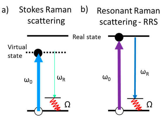
This review also focuses on alternative enhancement mechanisms for optical signals and collects cases where several mechanisms can be combined. One option to increase Raman signal is by tuning the excitation laser energy with that of real electronic transitions of the molecules to be detected, taking advantage of the resonant Raman scattering (RRS) process. A recent focus in this area is the search of SERS amplification platforms efficient in the UV, to combine SERS and RRS, based on several metals that present plasmon resonances in the UV, such as aluminum [22][23] or rhodium [24], but with much lower efficiency than that of silver or gold in the visible range [25]. Another enhancement mechanism that is reviewed here and which has been scarcely explored for Raman spectroscopy is related to the amplification of an electromagnetic signal based on interference processes. Multilayered heterostructures based on thin films of materials can be designed and fabricated to optimize the interference of light occurring at the interfaces and can be tuned depending on the application and the excitation wavelength. The interference-enhanced Raman scattering (IERS) was defined in the 1980s and was initially used to detect the phonons of inorganic ultra-thin films [26][27]. Since the discovery of the properties of exfoliated graphene, single-crystalline silicon wafers with a SiO2 layer, typically hundreds of nanometers thick, are commonly used to better visualize and differentiate graphene flakes with a different number of layers. Now, Si/SiO2 substrates are used for this purpose to increase the Raman signal of 2D (or few-layer) materials with Raman gains up to around 40 [28][29][30][31].
2. SERS in Noble Metal NPs
The literature on SERS is massive and excellent reviews have been published both on experimental and theoretical aspects (see for example [4][5][6][19][33]). Here we collect some general conclusions regarding the relevance of size and shape on the amplification capabilities and focus on less explored aspects which are the inter-NP distance and the ultra-small NP size limit.
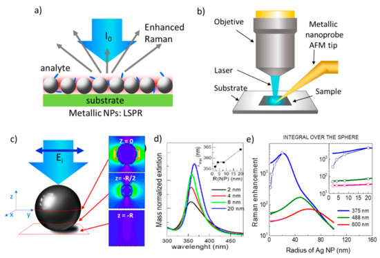
Local surface plasmon resonances (LSPR) occur in highly polarizable objects, such as nanosized metallic particles, that produce intense localized electric fields for specific incident light energies and originate huge enhancements of the Raman signals of vibration modes of molecules or phonons of solids when these are located in the NPs’ close vicinity (Figure 1a). In a first approximation, the LSPR electric field amplitude, E, decays as a dipole field, E ~ dm-NP−3, where dm-NP is the molecule-NP distance [4][34][35]. Experimentally, the optimum size of non-interacting spherical NPs is found to be in the range of 40–100 nm for gold and silver [36][37] but NPs’s optical properties strongly depend on their size, shape, and composition so that there is an intense activity to optimize these parameters [38][39][40][41].
Analytical calculations of optical extinction (absorption and scattering) can be obtained based on the Mie theory [42] which is exact for isolated spherical particles since it is a solution to Maxwell equations of plane waves impinging on metal/dielectric isolated spheres. In the case of non-spherical objects, the solution is much more complicated. In this case, it is possible to get an intuitive picture of the extinction process with non-interacting NPs using the dipolar approximation when the NP size is much smaller than the wavelength. For larger NPs multipolar terms should be taken into account together with electrodynamic corrections: the effect of the radiated field by induced dipoles. For metal NPs of very small sizes, surface damping plays an important role as the electron mean free path begins to approach the size of the nanoparticle, thus additional damping needs to be considered, in any of these approaches, by modifying the dielectric constant of the particle [32][33][34]. The extinction band correlates with the near-field electric field which originates the Raman enhancement.
Mie calculations for Ag NPs, show that the plasmon resonance as a function of NP diameter is red-shifted as the size increases, slightly (~8 nm) for NPs from 4 to 40 nm (Figure 1c) and more importantly for diameters > 40 nm with a significant widening and damping for these large NPs [38]. The most efficient plasmon for non-interacting Ag particles is calculated to be around 40 nm (diameter) however, it is located in the UV (~365 nm) which is not convenient for detection with Raman systems that use visible excitation. The LSPR spatial distribution of one NP is highly inhomogeneous and depends on the incident light polarization (Figure 1c), therefore, to obtain the averaged Raman amplification of n NP, which is the relevant value when the quantitative determination of molecule concentration is searched, it is necessary to integrate over the whole surface of the NP. Figure 1e shows such integrated Raman amplification using the dipolar approximation for the Mie theory, as a function of the NP radius for different incident excitation wavelengths. Indeed, the maximum amplification is obtained for NPs around 20 nm radius (40 nm diameter) when using laser excitation at 375 nm, but shifts to larger sizes for visible excitation wavelengths. The open circles show the results considering the damping effect for the small NP size end. The importance of the damping at the NP surface in the small limit is also visualized in the reduction of the resonance intensity when normalizing to the NP mass especially for radii below around 10 nm (Figure 1d) hampering SERS applications for the smallest non-interacting NPs.
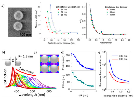
When two or more NPs are close enough, the electrical field distribution is no longer the addition of the electric fields associated with individual NPs and thus the NPs can no longer be considered as non-interacting. In this case, the particle size that maximizes the enhancement strongly varies depending on the details of the systems. The dependence of the overall enhancement on the inter-NP distance, d, is a complex problem since distributions of NPs size and of inter-NPs distances are usually present in real systems, and the formation of hot-spots occurring at the small gaps between adjacent NPs play a very relevant role (Figure 2). The electric field distribution around the NP is even more inhomogeneous when hot-spots are present [43], therefore the electric field at the particular position where the molecule is located relative to the NP can vary tremendously from one location to another (Figure 1d) so that the Raman signal will vary by orders of magnitude. When dealing with relatively high molecule concentrations the effect may be averaged but, for very low analyte concentrations the enhancement depends on the particular location of the tested molecules and the measured Raman signal will vary from one experiment to another. Thus, for extremely low concentrations SERS is intrinsically non-quantitative since it depends strongly on the particular location of the molecules on the NP surface. This tremendous electric field inhomogeneity is especially important for the lowest concertation, the detection of a single-molecule, which relies on hot-spots [44] to obtain the needed EF ~109 [45], and consequently, the experiments are not easily reproducible.
The use of simulations to obtain extinction and Raman amplification are necessary to analyze and understand the processes and foresee optimization directions. Commercial software packages are based on different approximations such as discrete dipole approximation (DDA), boundary element method (BEM), or finite-difference time-domain (FDTD). The discrete dipole approximation is an integral equation solver: particles of arbitrary shapes are modeled by a discrete set of polarizable dipoles, the electric field at each dipole includes that of the rest of the dipoles in the set. FDTD is a differential equation solver. To solve Maxwell differential equations, it uses the finite-difference method in the time domain so that time is also discretized. Solvers using FDTD have been more in use for the last 20 years. The difference between the two methods is mainly operational: how fast a complex system can be modeled and modified, this is probably why FDTD methods have gained more popularity. Also, the dependence on the frequency of the scattering and calculated fields is covered in a single simulation with FDTD methods. The boundary element method (BEM) is also an integral equation solver, it uses integral equation formulation and only needs the values of the fields on the boundary surfaces, the mesh in use is defined on the boundary surfaces and this makes this method less efficient than ordinary FDTD methods for large surface to volume ratios. It is not intended for nonlinear media.
Numerical simulations have to be utilized to include NP-NP interactions; it is then possible to obtain the dependence of the plasmon resonance as a function of the inter-NP distance for different NPs configurations. The calculation for NP pairs, ordered chains, or planes of NP arrays are feasible, but computing time increases dreadfully for large sets of disordered NPs [47][48]. However, state-of-the-art electromagnetic computation techniques can provide clues on the behavior of random arrangements of hundreds of NPs with different shapes.
The variation of the plasmon position was studied in lithographically fabricated pairs of Au nano-disks with inter-particle distances decreasing from 300 to 50 nm (Figure 2a). A red-shift up to 60 nm of the plasmon position as the inter-particle distance is reduced is observed and coincides with simulations using the discrete dipole approximation (DDA) [46]. In the ultra-small limit, the behavior of the simulated extinction spectra was reported for NP radii in the range from 2 to 10 nm when varying the inter-NP distance, d, in periodic arrays of silver NPs. The plasmon red-shifts, as in the case of the large Au disks, and also widens as d is reduced (Figure 2b). The changes in position and width of the plasmon resonance are significant (position shifts from 355 to >500 nm and width from 25 to >100 nm) and, when plotted against the inter-NP distance normalized to the NP radius, d/R, present an almost identical behavior for radii up to 10 nm (Figure 2d). Such red-shift and widening have been experimentally observed for 4 nm (diameter) randomly dispersed NPs [32]. A general rule is that proximity effects are important when the inter-NP distance is similar or lower than the particle diameter (d ≤ D = 2R). Simulations of NPs ordered arrays describe well randomly spread NPs and have the enormous advantage that the symmetry of periodic distributions allows for much shorter simulation times, but may be insufficient for wide inter-NP distance distributions.
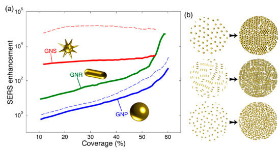
The relevance of the NP shape and the coverage (fraction of an NP-monolayer on a substrate), which is directly related to the average inter-NP distance, is shown in Figure 3. Solis et al. [47] have used a full-wave solution based on surface-integral equations (SIEs) discretized by the method of moments (MoM) to simulate such SERS platforms with hundreds of NPs. Shape is especially important for non-interacting particles: low coverages/large inter-NP distances. The asymmetry of the NPs and the presence of spikes [49] induce single-NP hot-spots (also called intrinsic electromagnetic hot-spots) that increase the EF [11]. As a practical example, tuning the aspect ratio of silver nanorods, which typically present two resonances, has been used to control the resonance wavelengths and reach the infrared range (related to the long axis of the rods), which is useful for different therapies [50]. For NPs without spikes, the reduction of inter-NP distances (increasing coverage or density) significantly increases the EF due to the formation of hot-spots at the NPs narrow gaps (Figure 3). Note that a coverage of 0.5 corresponds to an average inter-NP distance d ~ 2R for spheres. As the inter-particle distance is reduced, the EF increases by orders of magnitude (Figure 2e and Figure 3) overcoming the enhancement related to the hot-spots that originated at the spikes of individual NPs (Figure 3). Thus, at short inter-NP distances, the density of hot-spots is the dominant parameter over size and shape. It is in this regime where the ultra-small NPs (down to a few nm) becomes interesting to be used with visible excitation [32][51].
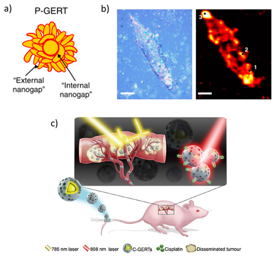
Complex core-shell NPs aggregates are designed to generate efficient hot-spots of great interest in biomaterials imaging, so-called gap-enhanced Raman tags (GERTs) (Figure 4a). The cells or tissues are previously stained with petal-like gold NPs aggregates whose morphology is controlled by some Raman reporter, which contains a thiol group to bind the gold NP (such as an aromatic dithiol), forming sub-nanometer internal gaps (red in Figure 4a). In the case of petal-like shell structures with an overall size of around 50 nm, the Au plasmon is red-shifted to ~600 nm and broadened due to plasmonic interactions between the close gold petals [52]. The highly enhanced Raman spectrum of the reporter at the nano-gaps inside the GERTs can be used to detect and image cells and tumors (Figure 4b,c) [53].
Individual plasmonic NPs are, in general, obtained by a chemical route such as the Lee and Meisel’s method [54], can be used as colloids, or can be randomly deposited and immobilized on different solid substrates, depending on the application [10][55][56]. Alternatively, a nanostructured film can be directly deposited on a substrate, typically by physical deposition techniques. An interesting approach to obtain very narrow NP size distributions on substrates is the gas aggregation sputtering technique [16][57][58] that avoids surfactants or any product but is limited to quite small NP sizes (<10 nm). Continuous films deposited on a substrate can be structured by different means such as the nanosphere lithography which is able to produce well-ordered 2D periodic NP arrays [59][60][61]. Indeed, the focus has recently been put on the creation of ordered plasmonic arrays since their optical properties can be tailored beyond size and shape with another parameter, the periodicity of the 2D and 3D structures and hence the inter-particle distance. In that way, plasmon-polariton modes, surface lattice resonance, or extraordinary transmission can be fostered and controlled. Lithographic techniques (such as laser interference, nanosphere, electron-beam, focused-ion, nanoimprint, or anodic aluminum oxide template, among others) offer a wide variety of scales and precision degrees to fabricate 2D and 3D ordered plasmonic structures. The rapid development of the fabrication techniques has endorsed size reduction of the plasmonic objects down to sub-nanometer scale, which are consequently governed by quantum interactions heading to the rise of quantum plasmonics [62].
3. Interference Raman Enhancement
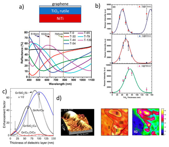
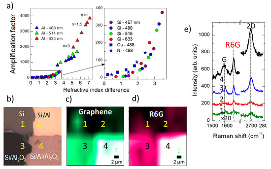
A proposed architecture, Si/Ag/Al2O3/graphene, includes silver as a reflecting layer and also as a plasmonic component to promote combined SERS and IERS amplification of the graphene signal, however with low EF ~ 20 [70]. Calculations to optimize IERS in reflecting/dielectric/graphene heterostructures indicate that the best situation occurs when the imaginary part of the reflecting layer refractive index is maximized and the real part for the dielectric layer is one. A universal correlation is found for the calculated EF (corresponding to the optimum dielectric thickness in each case) and the modulus of the complex refractive indices difference |Δn| = |n(dielectric) – n(reflector)| for all tested reflecting layers (Cu, Ni, Al, and Si) and for dielectric layers with a refractive index between 1 and 3 using typical excitation wavelengths in Raman spectroscopy (457, 488, 514, and 633 nm) (Figure 8a). It is concluded that the best experimentally easily accessible heterostructure is the combination of an aluminum film deposited on the extremely flat surface of a silicon wafer and a low-n oxide film, such as Al2O3 or SiO2. The calculated EF for Si/Al (90 nm)/Al2O3 (60 nm)/graphene system reaches 1200 for excitation at 488 nm and 104 for 1000 nm. The experimental EF at 488 nm is reported to be around 700 for the Raman peaks of the transferred graphene and slightly below for R6G Raman modes which were spin-coated on top (Figure 8b) [65].
In order to increase the EF, some studies report on the possibility to combine IERS and SERS mechanisms, [70] finding, however, relatively low amplification factors except when Ag NPs are deposited on top of Si/Al/Al2O3/Gr platforms where the combined enhancement is shown to be very efficient [65]. Other architectures have been recently proposed to enhance the Raman signal by increasing the specific area and thus the surface available for the molecules to be adsorbed, for example, by the combination of nano or micro-structured semiconductors (nanopillars, nanorods, etc.), with metallic NPs [71][72] or the formation of nanoporous metals [73].
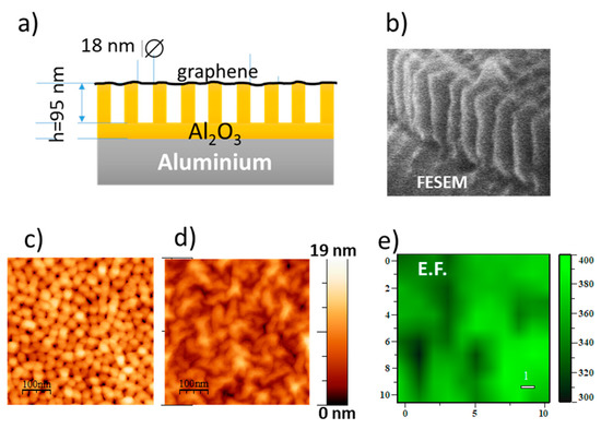
Graphene allows designing novel architectures such as interference platforms based on supported porous alumina membranes and graphene. Alumina and voids play the role of the dielectric layer, the aluminum foil at the base is the reflecting surface, and a transferred graphene single-layer on top serves to deposit the analyte on the voids (Figure 9). IERS with EF up to 400 and homogeneous amplification over the sample surface are obtained (Figure 9e) [74].
4. Fluorescence Enhancement and Imaging
There is a huge interest in enhancing PL signals, especially those originated from markers in biomaterials, to reduce the detection limits and to improve optical imaging. Simplified schemas of PL processes are presented in Figure 10. The first schema corresponds to the conduction to valence band emission in a solid without exciton formation. The other schemas correspond to luminescent molecules (also called chromophores, fluorophores or dyes) using the Jablonski diagrams where fluorescence and phosphorescence processes are shown (Figure 10a). After light absorption, and electron transition from the fundamental state with S = 0 (singlet) to an excited electronic (also with S = 0 since ΔS = 0 in an optical transition), the electron relaxes to the lowest vibrational state (red wavy line in Figure 10) of this excited electronic state (vibrational relaxation) and then radiatively decays to the fundamental state (fluorescence). However, molecules with high spin-orbit coupling have a higher probability to relax to an excited triplet state (S = 1) through the intersystem crossing mechanism (ISC). The radiative transition (phosphorescence) is spin forbidden so the lifetime of the triplet excited state is long as well as the lifetime of the emitted photons.
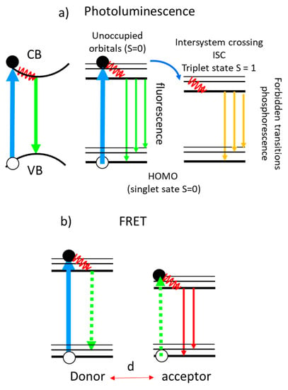
Important efforts have been devoted to study and optimize light enhancement using metallic substrates and NPs, also called metal-enhanced fluorescence (MEF) or surface-enhanced fluorescence (SEF), but the process is not totally understood and is many orders of magnitude less efficient than SERS. Enhancement factors below 15, typically, are reported for fluorescence both from experiments and calculations [75]. In many cases, the observed PL enhancement is mostly due to an increase in the absorption rates provided by the NPs that are acting as antennas rather than the modification of the spontaneous emission rates. The emission rate is related to the coupling of the emitter with the metal NP that involves many parameters such as the radiative and non-radiative decay rates of the emitter and of the NP, the quenching of the emitter by the metal, and the decay of the emitter by exciting plasmons [76]. Moreover, the interaction processes are strongly dependent on the emitter location relative to the NPs [77][78]. A reduction of the emission measured lifetime is usually observed due to new non-radiative de-excitation channels provided by the metal so that the fluorescent molecules have to be separated from the NPs by several nanometers to avoid total quenching. Fluorescence quenching by metal NPs is similar to that for graphene (Figure 6b). The process occurs by an energy transfer from the molecule to the metal without the participation of photons (the dashed vertical lines are virtual photons). This is a non-radiative process and is very similar to the Fluorescence or Förster Resonant Energy Transfer (FRET) described in Figure 10b between two molecules. FRET is due to a dipole-dipole interaction with a strong dependence on the distance between donor and acceptor (~1/d6) and on their spectral overlap (emission of the donor and absorption of the acceptor). FRET thus can occur for donor-acceptor distances typically below 10 nm [79]. Radiative transfer processes involve the emission of a photon that is afterward absorbed by an acceptor. FRET is commonly used to monitor biological reactions that occur at close distances by analyzing the fluorescence quenching induced by the involved processes.
Even if not comparable to SERS enhancement values, metal-enhanced fluorescence does improve signal detectability, increases intrinsic DNA fluorescence, and reduces blinking of single molecules [80]. A wide variety of fluorophores with different application fields have been tested. The fluorescence of individual CdTe quantum dots coated with PVA increases 5-fold when deposited on silver island films [14]. Metallic nanoporous Al-Mg alloys can be exploited for fluorescence enhancement in the deep UV [23]. Indeed, aluminum has been predicted to present the maximum plasmonic performance for UV [25].
Graphene and GO do not present fluorescence but have a role in fluorescence enhancement while graphene and GO quantum dots or nanodots (GQD), as well as carbon nanodots (CD), can produce efficient fluorescence emission, fostering interesting applications in biosensing. These graphene-related materials are adequate for theranostics by enabling fluorescence imaging combined with different therapeutic modalities [21][81]. Hereafter several applications of graphene derivatives are presented as examples of their convenience in bio-detection and imaging.
Among the variety of applications, graphene-related materials are attractive alternatives in the promising photodynamic therapy (PDT). Photodynamic therapy is based on the generation of highly reactive singlet oxygen by light irradiation of an injected photosensitizer to destroy target cells. The photosensitizers (PS) facilitate the fluorescence imaging and the time evolution upon light irradiation of the tissues modified by the generated singlet oxygen [82]. A variety of photosensitizers are used for photodynamic therapy, as liposomes and NPs of different nature (polymer, silica, magnetic, or gold), but their limited water solubility or fluorescence quenching are serious issues. Diverse strategies are being investigated to overcome these problems.
Regarding the role of GO, in many cases, when used as a nanocarrier of the photosensitizer, it produces fluorescence quenching. However, it can also promote and enhance fluorescence as in the developed nanoplatform based on GO -amine-terminated eight-arm branched PEG-DVDMS (photo-theranostic agent based on sinoporphyrin sodium). GO-PEG was demonstrated to enhanced the fluorescence of DVDMS. The emission is red-shifted and significantly enhanced, finding the maximum fluorescence yield for a relation 0.5:1 between GO-PEG and DVDMS (Figure 11a). These modifications are due to an intramolecular charge transfer within DVDMS mediated by its coupling to GO-PEG. The increased emission yield permits effective enhanced fluorescence imaging-guided photodynamic therapy for diagnosis and treatment of cancer (Figure 11b,c) [83].
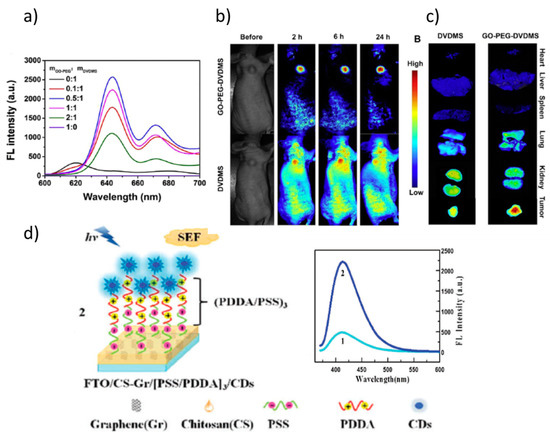
On their side, GQDs and CDs present efficient fluorescence associated with their nanometric size that can be tuned by modifying size and oxygen content. They are better suited for biological applications than most semiconductor quantum dots that contain heavy metal elements. GQDs are nanosized flakes (typically <10 nm) of few-layer graphene or graphene oxide [85] while CDs are almost spherical NPs (<10 nm) of sp2 C atoms that, mainly at the surface, present sp3 C linked to COOH and OH groups [86]. Both GQD and CD present remarkable photoluminescence (PL) properties, high water solubility, chemical inertness, and resistance to photobleaching. The functional groups present at the GQDs’ and CDs’ surface can be easily functionalized, are relatively stable, present tunable luminescence and low cytotoxicity, and thus good biocompatibility. The PL is due to bandgap transitions but their nature is still unclear [87]. An example of the combination of two uses of graphene derivatives is shown in Figure 11d. An enhancement of the fluorescence intensity of CDs has been demonstrated to be originated by the presence of a reduced GO layer, therefore without including metal NPs in the system (Figure 11d). The distance between the emitters (CDs) and the reduced GO layer was varied and optimized to maximize the CDs fluoresce quantum yield [84].
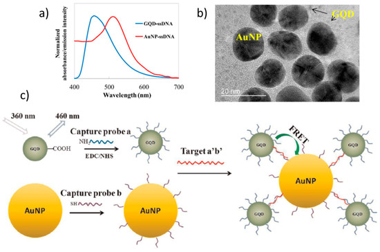
Graphene-related materials have also recently triggered studies on the possibilities they open for FRET applications (FRET mechanism is pictured in Figure 14b). FRET is extensively used in biosensing, in particular, to follow biological reactions that are occurring at close distances, such as antibody immunological recognition or DNA hybridization, by studying the fluorescence quenching occurring when donor and acceptor are close enough. So adequate and optimized donors and acceptors can enhance the sensitivity of FRET biosensors. Typically, fluorescent organic molecules and proteins have been used but their stability is poor and their photobleaching easy. Inorganic quantum dots and more recently graphene-related materials are being investigated [88]. Figure 12a shows that the spectral overlap of GQDs PL spectra and AuNPs absorption is adequate for FRET. When the target S. aureus gene oligo, formed by the union of amine-modified capture probes and reporter probes, becomes linked, the donor-acceptor distance is reduced and the quenching of the GQDs occurs (Figure 12c) [89].
These few examples are intended to show that graphene and its derivatives are in the focus for bioimaging and therapeutic applications however, their toxicity has to be carefully evaluated to be transferable to in vivo applications. Toxicity depends on several factors such as their size, shape, surface chemistry, and solubility since their physicochemical interactions and accumulation in specific organs vary depending on these properties [20][21][90]. A determining factor is the dose concentration, for example, in in-vitro experiments a dose concentration of 200 µg/mL of GO causes oxidative stress, inducing a loss of cell viability. However, low GO concentrations (10 µg/mL) do not enter the cells and have no obvious toxicity [91]. The impact on the toxicity of the size of the GO flakes has also been studied, finding that the smallest GO showed the highest hemolytic activity [92]. Toxicity was also studied by modifying reduced GO. Hydrophobic reduced GO tends to accumulate on the cell membrane in large amounts, inducing high reactive oxygen species stress which leads to cell apoptosis but, after functionalizing it with carboxyl groups to make it hydrophilic the toxicity was largely eliminated, indicating that water solubility may also influence the toxicity of reduced GO [93]. Surface modifications of GO and reduced GO with polymers are also possible solutions to the toxicity problem. For example, the hemolysis of GO obtained by sonication was significantly reduced with chitosan coating on its surface [92] and no cytotoxicity is found for GO after being modified with PEG [94].
Among other different approaches for fluorescence enhancement, the plasmonic nanocavities and the interference-based platforms are at initial development stages and graphene has been scarcely incorporated. The plasmonic nanocavities are usually formed at the gaps between a metallic surface and metallic NPs. The metallic surface, the NPs, or both are coated with a dielectric layer to avoid electric contact and the delocalization of the plasmons. This insulating layer is also required to avoid fluorescence quenching [78]. Complex experimental systems and mathematical treatments are being developed for single-molecule optical studies using plasmonic nanocavities [95][96] that allow nanometric spatial resolution, well below the theoretical diffraction limit for visible light (around 200 nm for 500 nm excitation wavelength).
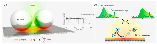
Recently, single-molecule modifications have been followed in real-time using a standard confocal Raman system and a plasmonic cavity formed by a silver surface coated with a 2 nm SiO2 layer and silver shell-isolated NPs (~60 nm Ag diameter) (Figure 13a) [97]. The photo-induced bond cleavage between the xanthene and phenyl group of a single rhodamine B isothiocyanate molecule is studied by combining Raman and fluorescence signals (Figure 13b). In addition, recently enhancements of the intensity of graphene Raman phonons and of graphene absorption have been reported when located in plasmonic nanocavities [98][99].
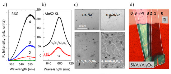
While the processes leading to Raman and PL enhancements in the vicinity of metallic NPs are different and generate very different EF; the interference mechanism is identical for Raman and fluorescence except that there is often a larger wavelength difference between the incident and scattered beams in the latter case. This detail has not an important impact since the refractive index variation on the typical wavelength ranges is usually moderate for the involved materials. However, scarce works have reported on the use of light interference for fluorescence enhancement but such platforms may be of interest for fluorescence bioimaging. EF as high as 100 was observed for R6G fluorescence signals (Figure 14a) when deposited on a Si/Al/Al2O3 heterostructure without graphene thus avoiding fluorescence quenching. Large enhancement factors, around 40 for Raman and 50 for PL, were also detected for single-layer MoS2 in a similar Si/Al/Al2O3 platform (Figure 14b). Moreover, these platforms strongly enhance the quality of the white light optical images. The wrinkles, two-layer micron-sized areas, and other defects in single-layer graphene obtained by CVD and transferred to such platforms are clearly seen (Figure 14c). In Figure 14d, single-layer MoS2, is clearly visualized on the platform (lower part of the image) and the regions with 2, 3 and 4 layers are well differentiated. On the contrary, MoS2 is almost undetectable (for 1and 2-layer MoS2) on silicon (upper part).
References
- Ren, B.; Lin, X.F.; Yang, Z.L.; Liu, G.K.; Aroca, R.F.; Mao, B.W.; Tian, Z.Q. Surface-Enhanced Raman Scattering in the Ultraviolet Spectral Region: UV-SERS on Rhodium and Ruthernium Electrodes. J. Am. Chem. Soc. 2003, 125, 9598–9599.
- Nemanich, R.J.; Tsai, C.C.; Conell, A.N. Interference-Enhanced Raman Scattering of Very Thin Titanium and Titanium Oxide Films. Phys. Rev. Lett. 1980, 44, 273–276.
- Connell, G.A.N.; Nemanich, R.J.; Tsai, C.C. Interference Enhanced Raman Scattering from Very Thin Absorbing Films. Appl. Phys. Lett. 1980, 36, 31–33.
- Wang, Y.Y.; Ni, Z.H.; Shen, Z.X.; Wang, H.M.; Wu, Y.H.; Wang, Y.Y.; Ni, Z.H.; Shen, Z.X. Interference Enhancement of Raman Signal of Graphene. Appl. Phys. Lett. 2008, 92, 043121.
- Yoon, D.; Moon, H.; Son, Y.-W.; Choi, J.S.; Park, B.H.; Cha, Y.H.; Kim, Y.D.; Cheong, H. Interference Effect on Raman Spectrum of Graphene on SiO2/Si. Phys. Rev. B 2009, 80, 125422.
- Ni, Z.; Wang, Y.; Yu, T.; Shen, Z. Raman Spectroscopy and Imaging of Graphene. Nano Res. 2008, 1, 273–291.
- Ren, W.; Saito, R.; Gao, L.; Zheng, F.; Wu, Z.; Liu, B.; Furukawa, M.; Zhao, J.; Chen, Z.; Cheng, H.-M. Edge Phonon State of Mono- and Few-Layer Graphene Nanoribbons Observed by Surface and Interference Co-Enhanced Raman Spectroscopy. Phys. Rev. B 2010, 81, 035412.
- Alvarez-Fraga, L.; Climent-Pascual, E.; Aguilar-Pujol, M.; Ramírez-Jiménez, R.; Jiménez-Villacorta, F.; Prieto, C.; de Andrés, A. Efficient heterostructures for combined interference and plasmon resonance Raman amplification. ACS Appl. Mater. Interfaces 2017, 9, 4119–4125.
- Solonenko, D.; Gordan, O.D.; Milekhin, A.; Panholzer, M.; Hingerl, K.; Zahn, D.R.T. Interference-Enhanced Raman Scattering of F 16 CuPc Thin Films. J. Phys. D Appl. Phys. 2016, 49, 115502.
- Abidi, I.H.; Cagang, A.A.; Tyagi, A.; Riaz, M.A.; Wu, R.; Sun, Q.; Luo, Z. Oxidized Nitinol Substrate for Interference Enhanced Raman Scattering of Monolayer. RSC Adv. 2016, 6, 7093–7100.
- Yin, X.; Li, Y.; Ke, F.; Lin, C.; Zhao, H.; Gan, L.; Luo, Z.; Zhao, R.; Heinz, T.F.; Hu, Z. Evolution of the Raman Spectrum of Graphene Grown on Copper upon Oxidation of the Substrate. Nano Res. 2014, 7, 1613–1622.
- Ramírez-Jiménez, R.; Álvarez-Fraga, L.; Jimenez-Villacorta, F.; Climent-Pascual, E.; Prieto, C.; de Andrés, A. Interference Enhanced Raman Effect in Graphene Bubbles. Carbon N. Y. 2016, 105, 556–565.
- Gao, L.; Ren, W.; Liu, B.; Saito, R.; Wu, Z.; Li, S. Surface and Interference Coenhanced Raman Scattering of Graphene. ACS Nano 2009, 3, 933–939.
- Schmidt, M.S.; Hübner, J.; Boisen, A. Large area fabrication of leaning silicon nanopillars for Surface Enhanced Raman Spectroscopy. Adv. Mater. 2012, 24, 11–18.
- Barbillon, G. Fabrication and SERS performances of metal/Si and metal/ZnO nanosensors: A review. Coatings 2019, 9, 86.
- Garoli, D.; Schirato, A.; Giovannini, G.; Cattarin, S.; Ponzellini, P.; Calandrini, E.; Zaccaria, R.P.; D’Amico, F.; Pachetti, M.; Yang, W.; et al. Galvanic replacement reaction as a route to prepare nanoporous aluminum for UV plasmonics. Nanomaterials 2020, 10, 102.
- Aguilar-Pujol, M.; Ramírez-Jiménez, R.; Xifre-Perez, E.; Cortijo-Campos, S.; Bartolomé, J.; Marsal, L.F.; De Andrés, A. Supported ultra-thin alumina membranes with graphene as efficient interference enhanced raman scattering platforms for sensing. Nanomaterials 2020, 10, 830.
- Sun, S.; Wu, L.; Bai, P.; Png, C.E. Fluorescence enhancement in visible light: Dielectric or noble metal? Phys. Chem. Chem. Phys. 2016, 18, 19324–19335.
- Pelton, M. Modified spontaneous emission in nanophotonic structures. Nat. Photonics 2015, 9, 427–435.
- Tóth, E.; Ungor, D.; Novák, T.; Ferenc, G.; Bánhelyi, B.; Csapó, E.; Erdélyi, M.; Csete, M. Mapping Fluorescence Enhancement of Plasmonic Nanorod Coupled Dye Molecules. Nanomaterials 2020, 10, 1048.
- Sun, S.; Rasskazov, I.L.; Scott Carney, P.; Zhang, T.; Moroz, A. The critical role of shell in enhanced fluorescence of metal-dielectric core-shell nanoparticles. J. Phys. Chem. C 2020, 124, 13365–13373.
- Forster, T. Energiewanderung und Fluoreszenz. Naturwissenschaften 1946, 33, 166–175.
- Ray, K.; Badugu, R.; Lakowicz, J.R. Langmuir-Blodgett Monolayers of Long-Chain NBD Derivatives on Silver Island Films: Well-Organized Probe Layer for the Metal-Enhanced Fluorescence Studies. J. Phys. Chem. B 2006, 110, 13499–13507.
- Ray, K.; Badugu, R.; Lakowicz, J.R. Metal-enhanced fluorescence from CdTe nanocrystals: A single-molecule fluorescence study. J. Am. Chem. Soc. 2006, 128, 8998–8999.
- Ponzellini, P.; Giovannini, G.; Cattarin, S.; Zaccaria, R.P.; Marras, S.; Prato, M.; Schirato, A.; D’Amico, F.; Calandrini, E.; De Angelis, F.; et al. Metallic Nanoporous Aluminum-Magnesium Alloy for UV-Enhanced Spectroscopy. J. Phys. Chem. C 2019, 123, 20287–20296.
- Sanz, J.M.; Ortiz, D.; De La Osa, R.A.; González, F.; Brown, A.S.; Losurdo, M.; Everitt, H.O.; Moreno, F. UV plasmonic behavior of various metal nanoparticles in the near- and far-field regimes: Geometry and substrate effects. J. Phys. Chem. C 2013, 117, 19606–19615.
- Tabish, T.A.; Scotton, C.J.; Ferguson, D.C.J.; Lin, L.; an der Veen, A.; Lowry, S.; Ali, M.; Jabeen, F.; Ali, M.; Winyard, P.G. Biocompatibility and toxicity of graphene quantum dots for potential application in photodynamic therapy. Nanomedicine 2018, 13, 1923–1937.
- Orecchioni, M.; Cabizza, R.; Bianco, A.; Delogu, L.G. Graphene as cancer theranostic tool: Progress and future challenges. Theranostics 2015, 5, 710–723.
- Lovell, J.F.; Liu, T.W.B.; Chen, J.; Zheng, G. Activatable Photosensitizers for Imaging and Therapy. Chem. Rev. 2010, 110, 2839–2857.
- Yan, X.; Niu, G.; Lin, J.; Jin, A.J.; Hu, H.; Tang, Y.; Zhang, Y.; Wu, A.; Lu, J.; Zhang, S.; et al. Enhanced fluorescence imaging guided photodynamic therapy of sinoporphyrin sodium loaded graphene oxide. Biomaterials 2015, 42, 94–102.
- Weng, W.; Sun, X.; Liu, B.; Shen, J. Enhanced fluorescence based on graphene self-assembled films and highly sensitive sensing for VB12. J. Mater. Chem. C 2018, 6, 4400–4408.
- Tabish, T.A.; Zhang, S. Graphene Quantum Dots: Syntheses, Properties, and Biological Applications. In Comprehensive Nanoscience and Nanotechnology, 2nd ed.; David, L., Andrews, R.H., Lipson, T.N., Eds.; Academic Press: Cambridge, MA, USA, 2016; pp. 171–192. ISBN 9780128122969.
- Li, H.; Kang, Z.; Liu, Y.; Lee, S.-T. Carbon nanodots: Synthesis, properties and applications. J. Mater. Chem. 2012, 22, 24230–24253.
- Bagra, B.; Zhang, W.; Zeng, Z.; Mabe, T.; Wei, J. Plasmon-Enhanced Fluorescence of Carbon Nanodots in Gold Nanoslit Cavities. Langmuir 2019, 35, 8903–8909.
- Tian, F.; Lyu, J.; Shi, J.; Yang, M. Graphene and graphene-like two-denominational materials based fluorescence resonance energy transfer (FRET) assays for biological applications. Biosens. Bioelectron. 2017, 89, 123–135.
- Shi, J.; Chan, C.; Pang, Y.; Ye, W.; Tian, F.; Lyu, J.; Zhang, Y.; Yang, M. A fluorescence resonance energy transfer (FRET) biosensor based on graphene quantum dots (GQDs) and gold nanoparticles (AuNPs) for the detection of mecA gene sequence of Staphylococcus aureus. Biosens. Bioelectron. 2015, 67, 595–600.
- Tabish, T.A.; Zhang, S.; Winyard, P.G. Developing the next generation of graphene-based platforms for cancer therapeutics: The potential role of reactive oxygen species. Redox Biol. 2018, 15, 34–40.
- Liu, J.; Dong, J.; Zhang, T.; Peng, Q. Graphene-based nanomaterials and their potentials in advanced drugdelivery and cancer therapy. J. Control. Release 2018, 286, 64–73.
- Chang, Y.; Yang, S.-T.; Liu, J.-H.; Dong, E.; Wang, Y.; Cao, A.; Liu, Y.; Wang, H. In vitro toxicity evaluation of graphene oxide on A549 cells. Toxicol. Lett. 2011, 200, 201–210.
- Liao, K.H.; Lin, Y.S.; Macosko, C.W.; Haynes, C.L. Cytotoxicity of graphene oxide and graphene in human erythrocytes and skin fibroblasts. ACS Appl. Mater. Interfaces 2011, 3, 2607–2615.
- Sasidharan, A.; Panchakarla, L.S.; Chandran, P.; Menon, D.; Nair, S.; Rao, C.N.; Koyakutty, M. Differential nano-bio interactions and toxicity effects of pristine versus functionalized graphene. Nanoscale 2011, 3, 2461–2464.
- Baek, A.; Baek, Y.M.; Kim, H.M.; Jun, B.H.; Kim, D.E. Polyethylene glycol-engrafted graphene oxide as biocompatible materials for peptide nucleic acid delivery into cells. Bioconjug. Chem. 2018, 29, 528.
- Zhang, R.; Zhang, Y.; Dong, Z.C.; Jiang, S.; Zhang, C.; Chen, L.G.; Zhang, L.; Liao, Y.; Aizpurua, J.M.; Luo, Y.; et al. Chemical mapping of a single molecule by plasmon-enhanced Raman scattering. Nature 2013, 498, 82–86.
- Chikkaraddy, R.; De Nijs, B.; Benz, F.; Barrow, S.J.; Scherman, O.A.; Rosta, E.; Demetriadou, A.; Fox, P.; Hess, O.; Baumberg, J.J. Single-molecule strong coupling at room temperature in plasmonic nanocavities. Nature 2016, 535, 127–130.
- Li, C.-Y.; Duan, S.; Yi, J.; Wang, C.; Radjenovic, P.M.; Tian, Z.-Q.; Li, F.J. Real-time detection of single-molecule reaction by plasmon-enhanced spectroscopy. Sci. Adv. 2020, 6, eaba6012.
- Li, X.; Zhang, T.; Fu, Z.; Kang, B.; Mi, X.; Sun, M.; Zhang, C.; Zhang, Z.; Zheng, H. Plasmonic nanocavity enhanced vibration of graphene by a radially polarized optical field. Nanophotonics 2020, 9, 2017–2023.
- Guo, S.; Zhang, D.; Zhou, J.; Deng, J.; Deng, J.; Yu, Y.; Cai, Q.; Li, Z.; Lu, W.; Chen, X. Enhanced infrared photoresponse induced by symmetry breaking in a hybrid structure of graphene and plasmonic nanocavities. Carbon 2020, 170, 49–58.

