| Version | Summary | Created by | Modification | Content Size | Created at | Operation |
|---|---|---|---|---|---|---|
| 1 | Kwok Wei Shah | + 1294 word(s) | 1294 | 2019-06-06 11:00:52 | | | |
| 2 | Bruce Ren | -7 word(s) | 1287 | 2020-10-29 10:07:27 | | |
Video Upload Options
The fundamental properties of a material can dramatically change when its dimensions are reduced nanometer scale. Metallic nanowires are one-dimensional nanostructures with diameters that are typically in a range of 10-200 nm, and lengths in a range of 5-100 µm. Metallic nanowires have many unique properties that are not seen in their bulk counterparts, such as good thermal and electrical conductivity, high aspect ratio, low sheet resistance, excellent optical transparency, etc. In the past two decades, research into metallic nanowires has encouraged breakthrough technologies in a variety of fields, including flexible transparent conductive films and electrodes, optoelectronic devices, molecular electronics, solar cells, touch screens, biomedical science, chemical sensors, heat transfer enhancement, etc.
1. Introduction
The great advancements achieved in the frontier of nanomaterial science has opened up a broad range of their applications [1]. As a useful one-dimensional (1D) nanostructure, metallic nanowires (NWs) have been extensively investigated for their unique properties, such as good thermal and electrical conductivity, high aspect ratio, good mechanical flexibility, excellent optical transparency, etc. On this basis, metallic NWs are being considered as multifunctional materials owing to their amazing behaviors, which are not seen in their bulk counterparts [2][3]. In the past two decades, research into 1D metallic NWs has encouraged breakthrough technologies in a variety of fields, including flexible transparent conductive films and electrodes [4][5][6], conductive polymer nanocomposites [7], touch sensors [8][9], photovoltaic (PV) cells [10][11], electrochromic devices (ECD) [12], wearable optoelectronic devices [13], and thermal energy storage (TES) [14]. The rapid advancement in the frontier of metallic NW technologies, particularly silver nanowires (AgNWs) and copper nanowires (CuNWs), has made them up-and-coming candidates for next generation engineering materials. Meanwhile, many synthesis methods have been developed to yield metallic NWs with uniform size at low cost thanks to the developed characterization techniques [15].
2. Synthesis techniques of metallic nanowires
Metallic NWs have been synthesized by means of different shape-controlled techniques, such as hard template method [15], soft template method [16][17], polyol method [18], hydrothermal method [19], electro-deposition method [20], ultraviolet (UV) irradiation route [21], wet reduction method [22], chemical vapor deposition (CVD) [23], etc. Among various metallic NWs, AgNWs and CuNWs are most widely studied and exploited, since they possess similar physical and chemical properties at room temperature.
3. Characterization of metallic nanowires
To characterize the morphology of metallic NWs, Transmission Electron Microscopy (TEM) and Scanning Electron Microscopy (SEM) are the most applied methods. The TEM and SEM provide useful information regarding the shape and size of metallic NWs. However it should be noted that the diameter of metallic NWs measured by SEM is usually higher than that from TEM due to the adherence of PVP on the NW’s surface [24]. High resolution TEM (HRTEM) provides the information of lattice spacing to obtain the crystal structure of metallic NWs. Other widely used methods include Atomic Force Microscopy (AFM) and X-ray Diffraction (XRD). The AFM can provide the surface topography and roughness of metallic NW networks. XRD is able to analyze the crystalline properties of metallic NWs.
4. Applications of metallic nanowires
4.1 Heat transfer enhancement
Due to their excellent thermal conductivity, metallic NWs can be used for heat transfer enhancement of solid or fluid. For example, since the building sector takes up almost 45% of energy consumption globally, enhancements to building energy efficiency and reduced reliance on air-conditioning systems is very important to achieve a sustainable future. Phase change materials (PCMs) are substances that absorb, store, and release thermal energy isothermally, and are therefore well suited for developing energy-efficient buildings, both actively and passively. The most commonly used solid-liquid PCMs fall into organic PCMs (e.g., paraffins and fatty acids) and inorganic PCMs (e.g., salt hydrates). However, the applications of PCMs are usually limited by their inherent low thermal conductivity, which could be overcome by dispersing thermally-conductive metallic NWs as the thermal conductivity promoter to improve the melting and freezing cycles.
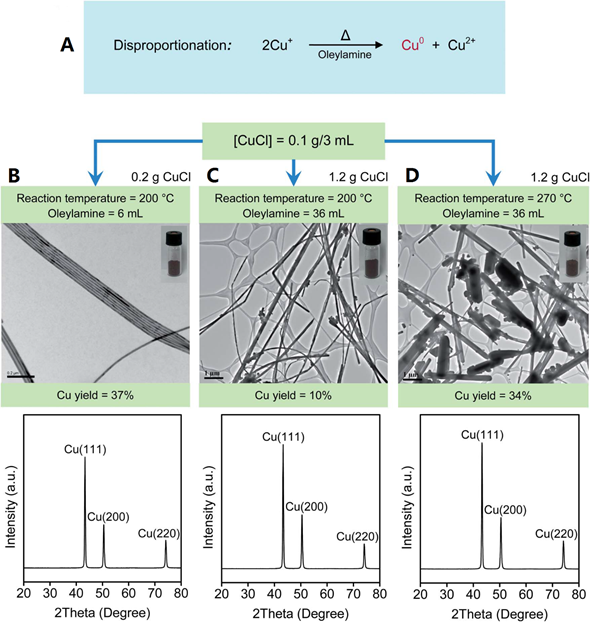
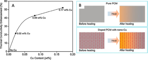
CuNWs, with their high thermal conductivities, have been used to develop nano-enhanced PCMs (NePCMs) for building applications. Shah et al. [14] prepared CuNWs by disproportionation of a Cu+ precursor in octadecylamine (ODA). After purification, reddish nanostructures were obtained, and their structures were verified by TEM and XRD, as shown in Figure 1. The prepared CuNWs were incorporated into a hydrated CaCl2∙6H2O salt-based PCM and the corresponding thermal conductivities at different concentrations of CuNWs were measured. Their results showed that just 0.02 wt.% of CuNWs increased thermal conductivities by >20%, although it should be noted that the effect of diminishing returns is also observed past 0.08 wt.% of CuNWs (Figure 2).

Figure 1. (A) Reaction for generating CuNWs. (B–D) Yield, morphology, and XRD pattern of CuNWs prepared at different conditions. Insets show the reddish CuNWs products after purification [14].

Figure 2. (A) Thermal conductivity enhancement of PCM (B). Schematic diagrams of heat transfer and dissipation in the pure PCM versus CuNW-doped PCM upon heating [14].
Similarly, one of the most important components in a building system is the air-conditioning, which heavily relies on the heat transfer between coolant and ambient air. However, most coolants, such as water, possess low thermal conductivity, leading to an increase in the system cost, since large surface area (e.g., mounting fins) is needed to ensure a high heat transfer efficiency. A similar situation also occurs in the harvesting of solar thermal energy. Metallic NWs can be suspended into the heat transfer fluid to form nanofluid which has a better heat transfer coefficient during heat exchange process.
4.2 Transparent conductive electrode
Due to their excellent electricity conductivity, optical transmittance and flexibility, metallic NWs can be used to fabricate transparent conductive electrodes (TCEs). The TCE is an important component in many modern electronics and they are usually made of indium tin oxide (ITO) and fluorine-doped tin oxide (FTO). However, the above materials were shown to be highly brittle, and thus not suitable for flexible TCEs [25]. On the other hand, ITO and FTO are expensive and the indium resources are becoming less abundant due to the increased consumption [26]. On this basis, metallic NWs can be applied to replace the ITO and FTO-based TCEs.
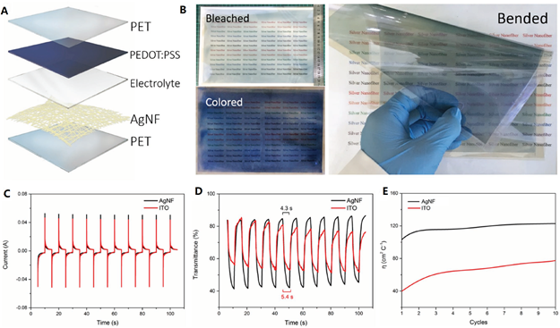
Lin et al. [27], for example, developed a nonheated roll-to-roll (R2R) technique to produce flexible, ultra-large, and transparent AgNW network electrode film. The main feature of this technique is that the precursor solution was rapidly stretched into NWs by UV irradiation and by adding polyvinylpyrrolidone (PVP). The reduction of Ag ions only took 3 h without heating. Figure 3 shows that amorphous carbon skeleton was attached on the surface of AgNW, which is due to the degradation of polymer and PVP. The authors pointed out that the skeleton can offer sufficient mechanical strength without affecting the electrical conductivity of AgNWs. The AgNW/polyethylene terephthalate (PET) film showed a sheet resistance of ~15 Ω sq−1 and transmittance of 95%. In comparison to ITO electrochromic window (ECW), the AgNW ECW showed a shorter switching time of coloration (4.3 vs. 5.4 s), a higher electron-transfer rate, and a higher coloration efficiency (120 vs. 80 cm2 C−1), as shown in Figure 4.

Figure 3. SEM image of AgNW network (scale bar 10 and 2 µm and 300 nm) [27].

Figure 4. (A) structural schematic of AgNW-based ECW, (B) flexible A4-sized ECW, (C) current response, (D) transmittance response, and (E) coloration efficiency during the first 10 switching cycles [27].
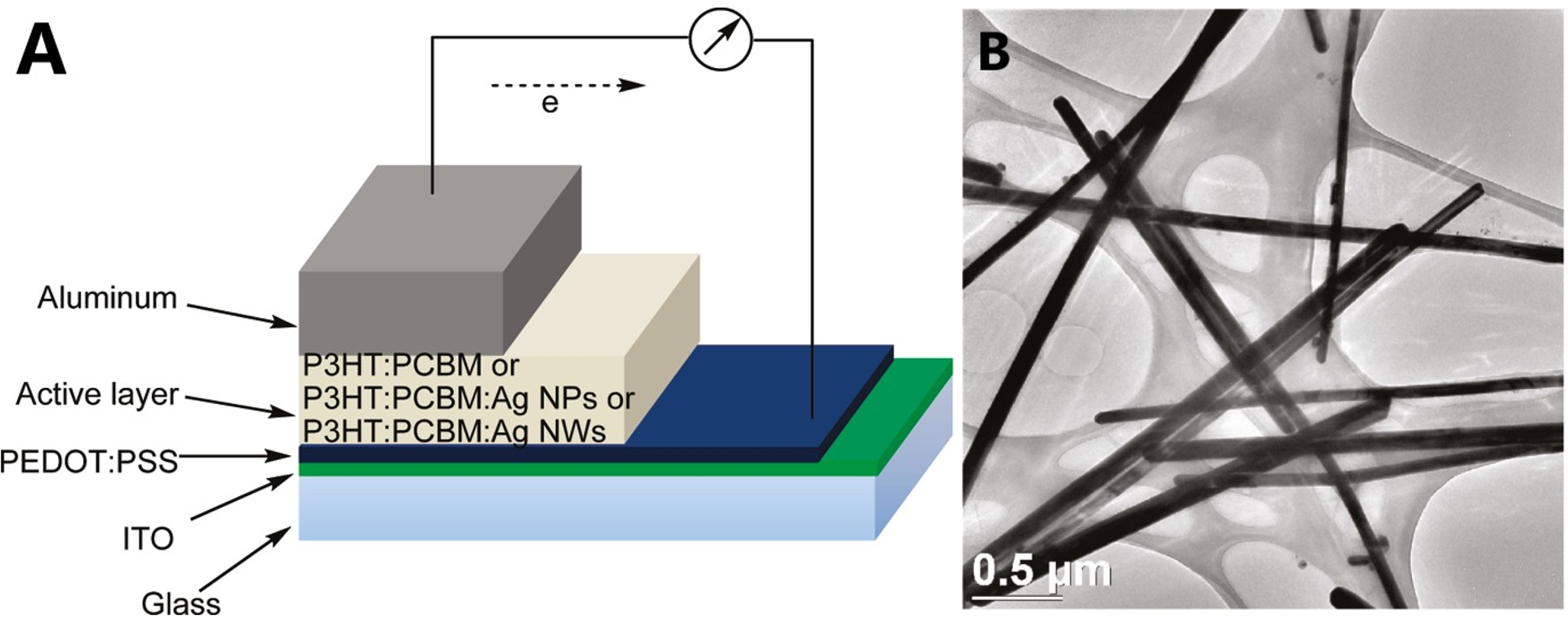
Metallic NWs-based TCEs can be also used in solar cells. For example, Kim et al. [28] have fabricated hybrid PV devices by a combination of poly(3-hexylthiophene) (P3HT) and [6,6]-phenyl C61-butyric acid methyl ester (PCBM) with ratio of 1:0.7. 20 wt.% of AgNWs, which was spin coated into the active to improve the photovoltaic (PV) performance, as shown in Figure 23. The AgNW-embedded PV device showed a power conversion efficiency (PCE) of 3.91%, high short-circuit current density (JSC) of 9.32 mA cm−2, fill factor (FF) of 63.6%, and open-circuit voltage (VOC) of 0.66 V.

Figure 5. (A) Layout of PV device and (B) TEM image of poly(3-hexylthiophene) (P3HT)-[6,6] phenyl C61-butyric acid methyl ester (PCBM):AgNWs structure [28].
References
- Qi Zhang; Qi-Kai Li; Mo Li; Internal stress and its effect on mechanical strength of metallic glass nanowires. Acta Materialia 2015, 91, 174-182, 10.1016/j.actamat.2015.03.029.
- Fevzihan Basarir; Farid Sayar Irani; Arif Kosemen; B. Tugba Camic; Faruk Oytun; Bahadir Tunaboylu; Hee Jeong Shin; Ki Young Nam; Hyosung Choi; Recent progresses on solution-processed silver nanowire based transparent conducting electrodes for organic solar cells. Materials Today Chemistry 2017, 3, 60-72, 10.1016/j.mtchem.2017.02.001.
- Kwok Wei Shah; Yong Lu; Morphology, large scale synthesis and building applications of copper nanomaterials. Construction and Building Materials 2018, 180, 544-578, 10.1016/j.conbuildmat.2018.05.159.
- Yin Cheng; Shouling Wang; Ranran Wang; Jing Sun; Lian Gao; Copper nanowire based transparent conductive films with high stability and superior stretchability. Journal of Materials Chemistry C 2014, 2, 5309-5316, 10.1039/c4tc00375f.
- Aaron R. Rathmell; Benjamin J. Wiley; The Synthesis and Coating of Long, Thin Copper Nanowires to Make Flexible, Transparent Conducting Films on Plastic Substrates. Advanced Materials 2011, 23, 4798-4803, 10.1002/adma.201102284.
- Yijie Xia; Kuan Sun; Jianyong Ouyang; Solution-Processed Metallic Conducting Polymer Films as Transparent Electrode of Optoelectronic Devices. Advanced Materials 2012, 24, 2436-2440, 10.1002/adma.201104795.
- Antoine Lonjon; Ivan Caffrey; Delphine Carponcin; Eric Dantras; Colette Lacabanne; High electrically conductive composites of Polyamide 11 filled with silver nanowires: Nanocomposites processing, mechanical and electrical analysis. Journal of Non-Crystalline Solids 2013, 376, 199-204, 10.1016/j.jnoncrysol.2013.05.020.
- Hsun-Chen Chu; Yen-Chen Chang; Yow Lin; Shu-Hao Chang; Wei-Chung Chang; Guo-An Li; Hsing-Yu Tuan; Spray-deposited Large-area Copper Nanowire Transparent Conductive Electrodes and their uses for Touch Screen Applications. ACS Applied Materials & Interfaces 2016, 8, 13009-13017, 10.1021/acsami.6b02652.
- Jinhwan Lee; Phillip Lee; Hyungman Lee; Dongjin Lee; Seung Seob Lee; Seung Hwan Ko; Very long Ag nanowire synthesis and its application in a highly transparent, conductive and flexible metal electrode touch panel. Nanoscale 2012, 4, 6408, 10.1039/c2nr31254a.
- Than Z. Oo; Nripan Mathews; Guichuan Xing; Bo Wu; Bengang Xing; Lydia H. Wong; Sum Tze Chien; Subodh G. Mhaisalkar; Ultrafine Gold Nanowire Networks as Plasmonic Antennae in Organic Photovoltaics. The Journal of Physical Chemistry C 2012, 116, 6453-6458, 10.1021/jp2099637.
- Gaute Otnes; Magnus T. Borgström; Towards high efficiency nanowire solar cells. Nano Today 2017, 12, 31-45, 10.1016/j.nantod.2016.10.007.
- Lianhuan Du; Liuxue Shen; Shaozao Tan; Zhigang Zang; Chuanxi Zhao; Wenjie Mai; Flexible electrochromic supercapacitor hybrid electrodes based on tungsten oxide films and silver nanowires. Chemical Communications 2016, 52, 6296-6299, 10.1039/C6CC01139J.
- Sukjoon Hong; Habeom Lee; Jinhwan Lee; Jinhyeong Kwon; Seungyong Han; Young D. Suh; Hyunmin Cho; Jaeho Shin; Junyeob Yeo; Seung Hwan Ko; et al. Highly Stretchable and Transparent Metal Nanowire Heater for Wearable Electronics Applications. Advanced Materials 2015, 27, 4744-4751, 10.1002/adma.201500917.
- Thammanoon Sreethawong; Kwok Wei Shah; Shuang-Yuan Zhang; Enyi Ye; Suo Hon Lim; Uma Maheswaran; Whey Ying Mao; Ming-Yong Han; Optimized production of copper nanostructures with high yields for efficient use as thermal conductivity-enhancing PCM dopant. Journal of Materials Chemistry A 2014, 2, 3417, 10.1039/c3ta14550f.
- Nasir M. Abbasi; Haojie Yu; Li Wang; Zain- Ul- Abdin; Wael A. Amer; Muhammad Akram; Hamad Khalid; Yongsheng Chen; Muhammad Saleem; Ruoli Sun; et al.Jie Shan Preparation of silver nanowires and their application in conducting polymer nanocomposites. Materials Chemistry and Physics 2015, 166, 1-15, 10.1016/j.matchemphys.2015.08.056.
- Dongbai Zhang; Limin Qi; Jiming Ma; Humin Cheng; Formation of Silver Nanowires in Aqueous Solutions of a Double-Hydrophilic Block Copolymer. Chemistry of Materials 2001, 13, 2753-2755, 10.1021/cm0105007.
- Jun-Jie Zhu; Xue-Hong Liao; Xiao-Ning Zhao; Hong-Yuan Chen; Preparation of silver nanorods by electrochemical methods. Materials Letters 2001, 49, 91-95, 10.1016/s0167-577x(00)00349-9.
- Y. Sun; Y. Xia; Large-Scale Synthesis of Uniform Silver Nanowires Through a Soft, Self-Seeding, Polyol Process. Advanced Materials 2002, 14, 833-837, 10.1002/1521-4095(20020605)14:11%3c833::AID-ADMA833%3e3.0.CO;2-K.
- Zhaoping Liu; You Yang; Jianbo Liang; Zhaokang Hu; Shu Li; Sheng Peng; Yitai Qian; Synthesis of Copper Nanowires via a Complex-Surfactant-Assisted Hydrothermal Reduction Process. The Journal of Physical Chemistry B 2003, 107, 12658-12661, 10.1021/jp036023s.
- Xiao-Jun Zheng; Zhi-Yuan Jiang; Zhao-Xiong Xie; Shu-Hong Zhang; Bing-Wei Mao; Lan-Sun Zheng; Growth of silver nanowires by an unconventional electrodeposition without template. Electrochemistry Communications 2007, 9, 629-632, 10.1016/j.elecom.2006.10.039.
- Lanlan Liu; ChaoDong He; Jia Li; Jinbao Guo; Dian Yang; Jie Wei; Green synthesis of silver nanowires via ultraviolet irradiation catalyzed by phosphomolybdic acid and their antibacterial properties. New Journal of Chemistry 2013, 37, 2179, 10.1039/c3nj00135k.
- Shenjie Li; Lijian Huang; Daocheng Pan; Yanyan Chen; Large-Scale Synthesis of Well-Dispersed Copper Nanowires in an Electric Pressure Cooker and Their Application in Transparent and Conductive Networks. Inorganic Chemistry 2014, 53, 4440-4444, 10.1021/ic500094b.
- Changwook Kim; Wenhua Gu; Martha Briceno; Ian M. Robertson; Hyungsoo Choi; Kyekyoon (Kevin) Kim; Copper Nanowires with a Five-Twinned Structure Grown by Chemical Vapor Deposition. Advanced Materials 2008, 20, 1859-1863, 10.1002/adma.200701460.
- Pei Zhang; Ian Wyman; Jiwen Hu; Shudong Lin; Zhiwei Zhong; Yuanyuan Tu; Zhengzhu Huang; Yanlong Wei; Silver nanowires: Synthesis technologies, growth mechanism and multifunctional applications. Materials Science and Engineering: B 2017, 223, 1-23, 10.1016/j.mseb.2017.05.002.
- Recep Yuksel; Zeynep Sarioba; Ali Cirpan; Pritesh Hiralal; Husnu Emrah Unalan; Transparent and Flexible Supercapacitors with Single Walled Carbon Nanotube Thin Film Electrodes. ACS Applied Materials & Interfaces 2014, 6, null-15439, 10.1021/am504021u.
- Akshay Kumar; Chongwu Zhou; The Race To Replace Tin-Doped Indium Oxide: Which Material Will Win?. ACS Nano 2010, 4, 11-14, 10.1021/nn901903b.
- Sen Lin; Xiaopeng Bai; Haiyang Wang; Haolun Wang; Jianan Song; Kai Huang; Chang Wang; Ning Wang; Bo Li; Ming Lei; et al.Hui Wu Roll-to-Roll Production of Transparent Silver-Nanofiber-Network Electrodes for Flexible Electrochromic Smart Windows. Advanced Materials 2017, 29, 1703238, 10.1002/adma.201703238.
- Chul-Hyun Kim; Sang-Ho Cha; Sung Chul Kim; Myungkwan Song; Jaebeom Lee; Won Suk Shin; Sang-Jin Moon; Joong Hwan Bahng; Nicholas A. Kotov; Sung-Ho Jin; et al. Silver Nanowire Embedded in P3HT:PCBM for High-Efficiency Hybrid Photovoltaic Device Applications. ACS Nano 2011, 5, 3319-3325, 10.1021/nn200469d.


