Your browser does not fully support modern features. Please upgrade for a smoother experience.
Submitted Successfully!
 +1 credit
Thank you for your contribution! You can also upload a video entry or images related to this topic.
For video creation, please contact our Academic Video Service.
| Version | Summary | Created by | Modification | Content Size | Created at | Operation |
|---|---|---|---|---|---|---|
| 1 | Anna Starczewska | -- | 7365 | 2024-03-25 10:43:05 | | | |
| 2 | Camila Xu | Meta information modification | 7365 | 2024-03-26 03:04:32 | | |
Video Upload Options
We provide professional Academic Video Service to translate complex research into visually appealing presentations. Would you like to try it?
Cite
If you have any further questions, please contact Encyclopedia Editorial Office.
Starczewska, A.; Kępińska, M. Photonic Crystals in Photovoltaics. Encyclopedia. Available online: https://encyclopedia.pub/entry/56471 (accessed on 14 June 2026).
Starczewska A, Kępińska M. Photonic Crystals in Photovoltaics. Encyclopedia. Available at: https://encyclopedia.pub/entry/56471. Accessed June 14, 2026.
Starczewska, Anna, Mirosława Kępińska. "Photonic Crystals in Photovoltaics" Encyclopedia, https://encyclopedia.pub/entry/56471 (accessed June 14, 2026).
Starczewska, A., & Kępińska, M. (2024, March 25). Photonic Crystals in Photovoltaics. In Encyclopedia. https://encyclopedia.pub/entry/56471
Starczewska, Anna and Mirosława Kępińska. "Photonic Crystals in Photovoltaics." Encyclopedia. Web. 25 March, 2024.
Copy Citation
Photonic crystals are artificial structures with a spatial periodicity of dielectric permittivity on the wavelength scale. These structures come in various materials and can be constructed in 1D, 2D, and 3D formats, providing a wide range of options for customizing the material's optical properties and potential applications. One of promising application is in the field of solar energy. By utilizing PCs in the design of solar cells, researchers can enhance their performance and efficiency by improving e.g., light management and increasing light trapping capabilities. This innovation can potentially significantly improve solar cells' effectiveness of all generations.
photonic crystal
photovoltaic
solar cell
1. Introduction
With increasing concerns over climate change, photovoltaics play a crucial role in the global transition to cleaner and more sustainable energy sources. Photovoltaics (PV) involve the conversion of light into usable electrical energy through photovoltaic cells, more often called solar cells (SC). Considering that the sun provides more than 10,000 times the current annual global energy consumption [1], researchers and engineers have focused on improving photovoltaic technology to make it more efficient, cost-effective, and widely applicable. The first practical solar cell was invented in 1954 by Bell Labs researchers [2]. It was made of silicon and had an efficiency of 6%. This breakthrough marked the beginning of photovoltaic technology, and currently, researchers are working on the fourth generation of solar cells [3]. Table 1 provides details of these generations.
| Generation | Type | Maximum Efficiency, %: | Literature about Using Photonic Crystals |
|---|---|---|---|
| First (Thick crystalline films) |
Monocrystalline silicon | 26.8 ± 0.4 [4] | |
| Multicrystalline/polycrystalline silicon | 23.3 [5] | ||
| III-V single junctions, e.g., GaAs thin film | 29.1 ± 0.6 [4] | ||
| Second (Thin films) |
Thin film chalcogenide (e.g., CIGS) | 23.35 ± 0.5 [4] | [6] |
| Amorphous silicon (a-Si) | 10.2 ± 0.3 [4] | [7] | |
| Microcrystalline silicon (mc-Si) | 11.9 ± 0.3 [4] | [8] | |
| Third (Emerging technologies) |
Dye-sensitized (DSSC) | 11.9 ± 0.4 [4] | [9] |
| Quantum dots (QDSC) | 18.1 [5] | [10] | |
| Organic (OSC) | 15.7 ± 0.3 [4] | [11] | |
| Perovskite (PSC) | 24.35 ± 0.5 [4] | [12] | |
| Multiple junctions, etc. (e.g., III–V 5J direct-bonded perovskite/Si cells) |
38.8 ± 1.2 [4] | [13] | |
| Fouth (Hybrid) |
Metal nanoparticles and metal oxides (e.g., hybrid silver/silver oxide nanoparticles in OSCs) | 5.2 [14] | [15] |
| Carbon nanotubes (e.g., CNTs in OSCs) | 14.37 [16] | [17] | |
| Graphene and its derivatives (e.g., MoS2 quantum dot/graphene with CH3NH3PbI3 perovskite) | 20.12 [18] | [19] |
There are several factors connected with the interaction of light and material that contribute to the restrictions on the efficiency of solar cells:
- -
-
Bandgap Limitation: The bandgap of a material determines the PV conversion band, which means the range of wavelengths it can absorb. Also, the type of band, direct or indirect, affects the efficiency.
- -
-
Absorption limit connected to reflection and transmission losses: Not all sunlight that strikes a solar cell can be absorbed and converted into electricity. Some wavelengths of light may pass through or be reflected, reducing the overall efficiency. The ray optics theory states that the absorption in a bulk solar cell’s structure should not surpass the so-called Lambertian limit by conventional light-trapping [20].
- -
-
Recombination: Charge carriers (electrons and holes) generated by absorbed photons can recombine before reaching the electrodes, leading to losses in efficiency.
- -
-
Thermalization Losses: When photons with energy higher than the material’s bandgap hit the solar cell, their excess energy can be lost as heat instead of being converted into electricity. This effect simultaneously leads to decreasing efficiency due to increasing recombination rates and changes in material properties.
Researchers and engineers are continually working to address these limitations through innovative designs, materials, and manufacturing techniques to improve the efficiency of solar cells and make them more cost-effective. Photonic crystals (PCs) are one of the best candidates for this purpose. Table 1 includes information concerning exemplary applications of PCs in various solar cells.
2. Photonic Crystals
Photonic crystals are artificial structures with a spatial periodicity of dielectric permittivity on the wavelength scale. This gives rise to Bragg diffraction, facilitating both constructive and destructive interference effects for certain wavelengths of light, leading to a photonic band gap (PBG). Within this spectral region, light is unable to propagate through the material. The existence of the PBG profoundly impacts interactions between light and matter, enabling phenomena such as light confinement, waveguiding, trapping, enhanced nonlinear effects, increased light emission, and the slow photon effect [21]. Periodicity can vary from one-dimensional to three-dimensional with a period of the order of the wavelength of light, and according to this, PCs can be categorized into one-dimensional (1D), two-dimensional (2D), and three-dimensional (3D) photonic crystals (Figure 1).
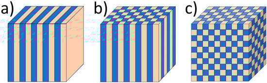
Figure 1. Models of photonic crystals: (a) one-dimensional (1D), (b) two-dimensional (2D), (c) three-dimensional (3D). The different colors represent materials with various refractive indices.
The spatial period of structure “a” is called the lattice constant, analogous to the lattice constant in ordinary crystals, built of regularly arranged atoms [21]. The interaction of light with such periodic structures depends on their geometry, i.e., both on the type of crystal lattice, the shape of elements located in the nodes of the lattice [22], and the volumetric share of the material with a given refractive index in the unit cell, quantified by the value called the filling factor, f [23]. Another crucial parameter affecting such periodic structures’ properties is the contrast of individual areas’ refractive indices. The most crucial feature of photonic crystals is the photonic band gap (PBG) in the photonic band structure. Its presence can be verified by examining the spectral characteristics of the reflection or transmission (Figure 2).
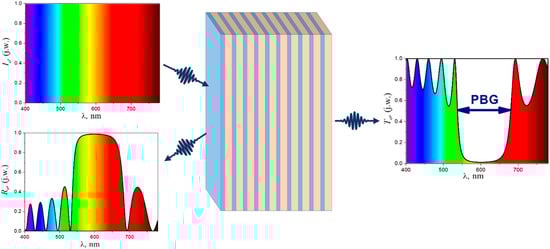
Figure 2. The Bragg mirror scheme and the reflectance and transmission spectra calculated for the Bragg mirror consist of 10 pairs of layers 75 nm thick and a refractive index of 2.0 and layers 100 nm thick and a refractive index of 1.5 [24].
1D PCs are otherwise called distributed Bragg reflectors (DBR) (Figure 2). Generally, they are designed as narrow-band reflectors.
Two types of 2D PCs can be distinguished [25][26]: photonic crystals of the “hole” type, consisting of cylinders with a low refractive index embedded in a medium with a high refractive index [27][28][29][30], and the “rod” type, consisting of rods with a high refractive index surrounded by a medium with a low refractive index [26][31][32][33][34][35][36]. Both holes and rods can be arranged differently to create different 2D crystal lattices. The main factors determining the properties of two-dimensional photonic crystals are the refractive index contrast, the degree of filling with a material with a high or low refractive index, and the type of crystal lattice. In 2D structures, the formation of a two-dimensional PBG requires the fulfillment of additional conditions [37][38], such as the appropriate geometry of the structure and a sufficiently high contrast of refractive indices [38][39][40]. The greater the contrast, the wider the total PBG is. Depending on the structure, the PBG may exist only for the TM or the TE mode [25][41][42]. Only in exceptional cases is a two-dimensional photonic band gap obtained for both polarizations [43][44], like in the “honeycomb” lattice.
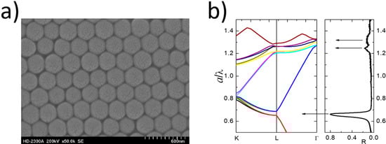
A large variety of 3D PCs exist. Some of the most popular are Yablonovite, consisting of a triangular system of holes prepared by drilling the slab at a specific angle, woodpile, formed “layer by layer” by a stock of dielectric 1D bars with alternating orthogonal orientations, opal or inverse opal, obtained by self-organization from monodisperse colloidal suspensions. Similar to 2D structures, the properties of 3D PCs depend on the geometry, degree of filling, and contrast in refractive indices [41]. An exemplary 3D photonic crystal in the form of SiO2 opal and its corresponding photonic band structure compared with reflection spectra are presented in Figure 3 [45].
3. Photonic Crystals in Photovoltaics
Photonic crystals can be applied in solar cells to enhance their performance and efficiency through better light management and trapping. They can be used as:
-
Anti-reflective and light-trapping surfaces
-
Back reflectors
-
Spectrum splitters
-
Absorption enhancers
-
Additional light management layers
-
Radiation coolers (RCs)
-
Electron transport layers (ETLs)
Table 2 presents the PCE values for examples of SCs with PCs and their percentage increase compared to SCs without PCs.
Table 2. The values of power conversion efficiency (PCE) and its increase (ΔPCE) as a result of the use of PCs. For comparison, the values of ΔPCE were calculated according to the formula (PCEPC−PCEr)/PCEr where PCEPC is the efficiency of SCs with PCs and PCEr is the efficiency of reference SCs without PCs. *: value is taken from the reference literature.
| Reference | Solar Cell | Type of PC | Function of PC | PCE, % | ΔPCE, % | Methodology |
|---|---|---|---|---|---|---|
| [47] | Perovskite | 2D honeycomb-like | Light management | 20.85 | 12.1 | Experimental |
| [48] | c-Si | 2D parabolic-pore inverted pyramid | Light trapping | 29.11 | 6.8 | Theoretical |
| [49] | c-Si | 3D inverse opal | Back reflectors | 30.43 | 16.0 | Theoretical |
| [50] | Thin film CdTe | 2D lattice of rods | Back reflector | 25.51 | 23.1 | Theoretical |
| [51] | CdS/CdTe-based | 1D multilayer | Back reflector | 10.47 | 26.7 | Experimental |
| [52] | Polymer | 1D multilayer | Back reflector | 8.20 5.41 |
23.3 26.4 |
Experimental |
| [53] | Perovskite | 2D lattice of rods | Absorption enhancer | 20.97 | 20.9 | Theoretical |
| [54] | Dye-sensitized | 3D inverse opal | Absorption enhancer | 6.875 | 21.7 | Experimental |
| [55] | Organic | 1D multilayer | RC | 8.98 | 1.5 | Theoretical |
| [55] | Perovskite | 1D multilayer | RC | 12.5 | 2.4 | Theoretical |
| [56] | Thin-film c-Si | 1D multilayer with the SiO2 grating | RC | - | 0.45 * | Theoretical |
| [57] | Hybrid perovskite | 3D inverse opal | ETL | 13.11 | 19.2 | Theoretical |
| [58] | Perovskite | 2D lattice of hemispheres | ETL | 15.2 | 44.7 | Experimental |
| [12] | Perovskite | 2D array of nanodisks | ETL | 18.70 | 19.6 | Experimental |
3.1. Anti-Reflective and Light-Trapping Surface
When electromagnetic radiation falls on the interface of two transparent media, generally, two phenomena occur: Part of the radiation passes from one medium to another, undergoing refraction, and the rest reflects from the interface. The more radiation is reflected, the less radiation passes inside. The bare silicon, still the most common material used in solar cells, in intimate contact with air, reflects approximately 35% of the incident power over all wavelengths used in solar cell work [60]. Thus, applying anti-reflective coating (ARC) or surface texturization is crucial to improve the efficiency of a solar cell [61][62]. They aid in preventing reflection and ensure as much radiation as possible penetrates the active layer, particularly of the wavelength range that interacts with the given material.
Different antireflection coatings have been optimized theoretically and experimentally so far (Figure 4). The simplest ARC consists of a thin layer of dielectric material (Figure 4a) with a specially chosen thickness so that interference effects in the coating cause the wave reflected from the ARC top surface to be out of phase with the wave reflected from the semiconductor surfaces [63]. The layer type and thickness depend on the material used in a solar cell. The dielectric contrast between the air and material of the solar cell should be reduced to reduce the reflection spectrum [64]. For instance, Fedawy et al. [63] examined the efficiency of GaAs solar cells covered with a Si3N4 antireflection layer. They increased efficiency from 14.89% to 27.16% by adding 75 nm Si3N4 ARC and 29.57% after additional front surface texturing (Figure 4b).
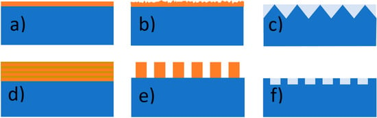
Figure 4. Different anti-reflective and light trapping surfaces: (a) interference thin film; (b) texturized thin film; (c) texturization in the form of a regular set of, e.g., micropyramids; (d) 1D photonic crystal; (e) rod-type 2D photonic crystal (f) hole-type 2D photonic crystal.
In the 1980s, Green et al. had already conducted a computer-based analysis of a double-layer antireflection phenomenon [61]. They found that a combination of a quarter wavelength of ZnS (refractive index, n = 2.25–2.35) and a quarter wavelength of MgF2 (n = 1.35–1.40) provided the best results (both thicknesses referred to a vacuum wavelength of 600 nm) in the case of silicon solar cells. It is possible to keep reflection loss below 2% from 460 to 940 nm with such a coating [61]. Multilayer antireflection structures (Figure 4d) have also been analyzed [65][66]. Womack et al. found that stacks of two SiO2 and two ZnO2 alternating layers of various thicknesses on thin film CdTe solar cells reduced their average reflection to ~1.2% [65]. Multilayer systems can be referred to as 1D PCs, provided that the periodicity of the layer system is maintained. These structures, commonly called distributed Bragg reflectors, are typically engineered to serve as narrow-band reflectors. However, their transmittance is almost negligible in the photonic band gap range wavelength. Regardless, applying 1D PCs as an ARC has been considered [62][64][67][68][69][70]. The consideration is often limited to the one-period photonic crystal structures [64][67][68][70], meaning multilayer structures are analyzed. The details of the examined 1D structure are presented in Table 3. Most of the works concern only theoretical considerations. An attempt to obtain the analyzed structure was made by Bennet’s group [69]. They used reactive sputtering to fabricate non-stoichiometric silicon oxynitride (SixOyNz) layers whose refractive index ranges typically from 1.4 to 1.7, depending on content.
Table 3. Details of 1D PCs theoretically analyzed as ARC.
| Reference | Type | No. of Periods | Materials | Optimum Thickness | Solar Cell |
|---|---|---|---|---|---|
| [67] | Ternary | 1 | SiO2/Si3N3/SiO2 | 98 nm/48 nm/8 nm | PIN silicon |
| [68] | Ternary | 1 | SiO2/KBr/SiO2 | 98 nm/48 nm/8 nm | PIN silicon |
| [69] | Binary | 1 or 2 | SixOyNz | a-Si:H | |
| [64] | Binary | 1 | SiO2/TiO2 | 54 nm/82 nm | a-Si |
| [64] | Ternary | 1 | SiO2/Si3N3/TiO2 | 54 nm/33 nm/82 nm | a-Si |
| [62] | Ternary | 1 | SiO2/Al:ZnO/SiO2 | 98 nm/48 nm/8 nm | a-Si:H |
| [62] | Ternary | 1 | SiO2/SiON/SiO2 | 98 nm/48 nm/8 nm | a-Si:H |
| [70] | Binary | MgF2/ZnS | 92.39 nm/54.95 nm 92.39 nm/109.91 nm |
||
| [70] | Ternary | MgF2/ZnS/Al2O3 | 92.39 nm/109.91 nm/ 78.70 nm |
Generally, better results were achieved in the case of ternary 1D PCs (e.g., [64]). To enhance the absorption, the authors of [64] combined multilayer ARC with inverted pyramid texturing on the top layer.
Two-dimensional photonic crystals (see, for example, Figure 4e,f) can also be utilized for antireflection [71][72][73] and light trapping [48][74][75][76][77] covers (see Table 4). Two main types of optical effects are commonly used in such structures: one based on geometric optics and the other based on wave optics [78]. The first relates to the shape conducive to multireflection and consequently improves absorption. The second approach is based on the peculiar properties of photonic crystals.
Table 4. Details of 2D PCs used as anti-reflective and light-trapping surfaces.
| Reference | Type of 2D PC | Lattice | Solar Cell | Methodology |
|---|---|---|---|---|
| [71] | Tapered silicon | Hexagonal a = 375 nm | Theoretical and experimental | |
| [72] | Round pillars Cones Round pillars Square pillars Inverted pyramids Round holes Round holes Square holes |
Square Square Hexagonal Rectangular Square Square Hexagonal Square |
On <100> silicon | Theoretical and experimental |
| [76] | Holes in ITO/p-AlGaAs layer | Hexagonal | GaAs | Theoretical |
| [73] | Nanocylinders of Al2O3 or PMMA | Square a = 440 nm |
GaAs Si |
Theoretical |
| [74] | Inverted nanopyramid surface texture | Thin-film c-Si | Theoretical and experimental | |
| [75] | Teepee-like PC | a = 1200 nm | c-Si | |
| [48] | Parabolic-pore thin-c-Si inverted pyramid |
a = 1000 nm | Thin-film c-Si | Theoretical |
| [77] | Inverted micropyramid surface texture | a = 1300 nm, 1800 nm, 2100 nm, and 2500 nm, |
Thin-film c-Si | Theoretical |
In 2010, Hung et al. [71] applied 2D PCs with tapered rods to achieve antireflection and enhanced absorption. That structure reduces the reflection due to a gradually changed effective index. On the other hand, strong optical resonances for TM-mode can be found in this structure, mainly due to the complete photonic band gap inside the material. Such resonance can enhance the optical absorption inside the silicon PCs due to its increased optical paths [71]. In 2013, surfaces with micropyramids (Figure 4c) were used in commercial solar cells as part of an antireflection strategy [72]. Dominguez et al. [72] optimized 2D photonic crystals (PCs) onto Si wafers to improve the performance of c-Si solar cells. Their objective was to find a structure capable of minimizing the reflectance of the Si wafer in the spectral range between 400 nm and 1000 nm. They analyzed both hole-type and rod-type 2D PCs (see Figure 4e,f) with different shapes of holes (inverted pyramids, square holes, round holes) and rods (round pillars, cones, square pillars) and different crystal lattices (square, hexagonal, rectangular) [72]. The pattern of circular pillars arranged in a square lattice with a pitch of 448 nm, a diameter of 325 nm, and a height of 138 nm (a) was found to be the best structure, with an average reflectance of 3.6% in the spectral region from 400 nm to 1000 nm. This value was obtained without any other material used as an anti-reflective coating.
Shen Hong-Jun et al. [79] designed a solar cell with an antireflection layer in the form of regularly arranged dielectric cylinders with a truncated cone shape. They used Si3N4 to form cones and SiO2 as a substrate. [78]. Kuang et al. [75][80] proposed a unique teepee-like PC on crystalline silicon (c-Si). This structure is characterized by excellent antireflection due to its Gaussian-type gradient index profile. It also enhances light trapping due to its near-orthogonal energy flow and vortex-like field concentration via the parallel-to-interface refraction effect inside the structure. On the other hand, the structure optimized for light-trapping, e.g., a teepee-like structure, may act as a surface recombination center and reduce solar cell efficiency [77]. Bhattacharya and John state that the most likely candidate for high-efficiency silicon solar cells consists of inverted micropyramid PCs [81].
It is worth mentioning that some authors treat inverted pyramid structures as a type of texture [64][82], while others treat them as PCs [83][84][85], calling them surface PCs [85]. If the lattice spacing is comparable to the desired wavelength, light trapping should be enhanced by robust wave interference in the photonic structure [83] and resonant effects [85]. However, according to Razzaq et al. [86], the influence on the efficiency of random pyramid texturing is comparable with a periodic inverted nanopyramid structure. A further study [87] showed that an optimized inverse nanopyramid regular structure could outperform the random pyramid texture when considering incidence angle variations.
These structures, playing the role of ARC, simultaneously contribute to light trapping, absorption enhancement, radiation cooling, etc.
3.2. Back Reflector
It is vital to prevent light from escaping from the active layer without being absorbed. This condition requires a relatively thick active layer (even up to 3 mm) in most popular silicon solar cells [88]). Back reflectors are applied to reduce this thickness. They reflect the light passing through the active layer back to the active region and enhance the path along which light can be absorbed. The simplest back reflectors are metal layers [76][89], for example, Ag [75][88] or Al [88][90]. However, they have some drawbacks (plasmonic resonance loss of the interface between the metal and absorption layers, performance degeneration due to metal ion diffusion) [88]. PCs find their application in thin film solar cells by providing controllable and enhanced reflections from material layers to promote increased absorption. The wavelength range and intensity of reflection depend on the PBG and can be easily adjusted thanks to a geometrical dimension of the PC structure. It allows for the easy optimization of 1D PCs concerning specific requirements.
There have been a large number of propositions for using PCs as a back reflectors (Figure 5):
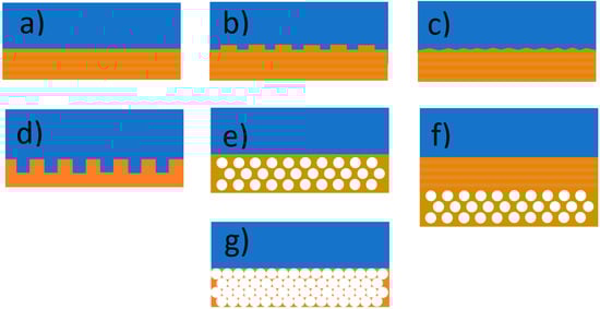
Figure 5. Different photonic crystal back reflectors: (a) 1D (DBR); (b) 1D with a reflection grating; (c) textured 1D; (d,e) 2D; (f) the combination of 1D and 2D; (g) 3D inverse opal.
Thanks to the PBG, photonic crystals can reflect up to 100% [89][97] of incident light over the PBG wavelength range. That is challenging to achieve using metal and dielectric mirrors. One condition is that this phenomenon refers only to the wavelengths in the range of the PBG. The key parameter for optimizing the PC design consists of adjusting the reflection peak (Bragg peak) to the solar photon energy to reflect it. This structure should reflect light within the range where the active material responds most efficiently.
Zeng et al. [100] and Zhou et al. [101] analyzed the combination of 1D PCs as a DBR and conventional [100] or 2D PC [101] reflection grating. With such a combination, the authors of [101] efficiently harvested solar photons without losses associated with textured metallic reflectors. They demonstrated that for near band edge photons, the optimized solar cells reach more than a hundred-fold increase in path length at diffraction resonances and exceed the classical light path enhancement limit predicted for randomly roughened interfaces.
Chen et al. [102] proposed another light trapping scheme based on a textured conductive photonic crystal (TCPC) back reflector in an n-i-p hydrogenated amorphous silicon (a-Si:H) solar cell. TCPCs combine a flat 1D PC and a randomly textured layer of chemically etched ZnO:Al. Total efficiency enhancement was obtained thanks to the sufficient conductivity, high reflectivity, and intense light scattering of the TCPC back reflector.
The other proposition of using a 2D PC as a back reflector for CdTe solar cells is presented in [50]. The proposed 2D structure has a hexagonal lattice of Ge rods placed in the SiO2 background. A device supplemented with such a structure has approximately 5% more power conversion efficiency than solar cells with metal back reflectors.
Zhan and Cai [88] obtained a back reflector in a full-wave band of 470–1100 nm by combining 1D and 2D PCs. The applied 1D PC was SiO2/c-Si DBR, and the 2D PC was a crystalline silicon slab with etched periodic air pores. The reflectivity of it is calculated to be 97.85%. Considering only the 2D PC and a range of 800–1100 nm, they achieved 99.32% reflectivity.
Varghese et al. [104] experimentally demonstrated a-Si inverse opal PCs as back reflectors for Si solar cells. The authors observed increased absorption of near-IR wavelengths and a 10% enhancement in the short-circuit current with no degradation in the open-circuit voltage. Additionally, they proposed simplifying the PC integration with a solar cell by transferring the free-standing PC membrane to form the PC onto electrically contacted cells. Simulations performed by the authors of [49] on such c-Si solar cells with inverse opal indicated the best effects were obtained for spheres with a diameter of 1 μm. The power conversion efficiency reached 30.4% compared with 20.95% without a back reflector.
3.3. Spectrum Splitter
Tandem solar cells are created for conversion power over a wide energy spectrum. Such cells consist of two or more layers of material having different energy gaps. The layer with the higher energy gap is placed at the top, and the layer with the lower energy gap is placed at the bottom (Figure 6). The most commonly used combination of materials is c-Si and a-Si [105]. Such a structure requires an additional intermediate reflected layer (IRL) for spectrum splitting and light management between these layers. The non-absorbed photons with shorter wavelengths should be reflected to the top layer of the solar cell, and the photons with longer wavelengths should be transmitted to the bottom one [62]. Photonic crystals are perfect for designing an IRL (see Figure 2). Moreover, the IRL must possess adequate electrical conductivity to prevent any losses through ohmic resistance in the interconnection of the active layers [106].
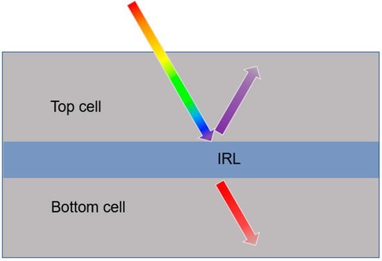
Figure 6. Schematic light propagation through a tandem solar cell structure with IRL.
1D multilayer structures [62][107], 1D photonic ribbon structures [108], and 3D inverse opals [106][107][109] as IRLs have been considered theoretically and experimentally. O’Brien et al. [107] compared solar cells’ properties with different IRLs, like 1.5-bilayer and 3.5-bilayer μc-Si/ZnO (acting as Bragg reflectors) and ZnO inverse opal. One of their conclusions was that the Bragg reflectors provide a larger band gap and less parasitic absorption than the analyzed inverted opal PC. The constituent materials of 1D binary PCs designed for c-Si/a-Si tandem solar by Sayed et al. [62] were Bi4Ge3O12 and μc-SiOx:H. They examined ten-period structures consisting of a 62 nm layer of Bi4Ge3O12 and μc-SiOx:H layers with different thicknesses (40 nm, 55 nm, and 73 nm) depending on the sample. However, they observed the widest PBG (400–730 nm) when stacked with all three structures.
Sundar et al. [105] theoretically designed a 1D magnetic photonic crystal (MPC) as a multilayer system of a metal-doped magnetic composite material (Cu-YIG) and μc-SiOx:H. They found that the photonic bandgap of MPC increases with the number of periods and the percentage of copper doping, which tends to enhance the light trapping in tandem solar cells.
A completely different 1D structure was demonstrated by Amiri et al. [108]. It was a one-dimensional silicon strip with a 200 nm breadth and a length of 18 μm with ten air holes etched on it. The air hole diameter was 180 nm and the lattice spacing was 1.75 μm. The structure parameters were matched to reflect the light of wavelengths from the specific range thanks to a photonic band gap. The reflected signal was absorbed by the upper cell, and the transmitted signal was absorbed by the bottom cell.
The other type of investigated IRL is inverse opal [106][107][109]. In 2008, Bielawny et al. [106] prepared a thin film of ZnO inverse opal at the rear side of a-Si solar cells with the intention of later integration with c-Si/a-Si tandem solar cells. Upping et al. [109] examined the impact of the IRL in the form of ZnO:Al inverse opal on the c-Si/a-Si tandem solar cell external quantum efficiency. They reported an increase in the enhancement of the external quantum efficiency in the a-Si:H layer with a factor of 3.6.
3.4. Absorption Enhancer
The Lambertian limit serves as a crucial benchmark in assessing the efficiency of solar cells [110]. Research has indicated that both extremely thick and extremely thin solar cells can approach this limit by implementing effective photon management strategies. By optimizing techniques for managing photons, these cells can operate closer to the Lambertian limit, resulting in improved overall performance. One way to enhance absorption is to use an active layer of SC in the form of a PC. Ordered photonic crystals have highly localized diffraction profiles and offer strong coupling to optical modes at specific wavelengths, with corresponding absorption enhancements that can exceed the Lambertian limit [111]. A periodic structure leads to nonlinear dispersion, which results in flat photonic bands and the appearance of band gaps in photonic crystals. The group velocity of light with wavelengths close to band gaps is anomalously low, and the so-called slow photon effect is observed [112]. The lower light velocity increases the effective optical path of light [113]. Thus, when the edge of the PBG overlaps with the electron absorption edge, the result can be expected to enhance light absorption [113]. The absorption edge can be tuned by varying the dimensions of the periodic structure, thereby moving the PBG [114]. This effect occurs for the photonic band gap’s red and blue edge [115]. Many authors explain absorption enhancement by the existence of slow photons [11][115][116][117][118]. However, Mihi and Miguez [115], examining dye-sensitized SCs as a combination of a photonic crystal and a layer of nanocrystalline absorbing material, concluded that absorption enhancement due to resonant modes localized within the absorbing coating brings a better effect than slow photons in the active layer of the PC form. Therefore, photonic crystals play only the role of porous colloidal mirrors operating through coherent scattering [115][119]. Coupling to the resonant modes was also considered by other authors [85][110][120][121], even in the case of the PC active layer [121]. Another explanation based on tuning the coupling strength of incident radiation to quasi-guided modes over a broad spectral range using the PC structure appears in refs. [122][123][124][125]. Such coupling enables the photons to spend enough time in the patterned active layer to be absorbed there [121]. The other mechanism for absorption enhancement in photonic crystals arises from strong resonances from parallel interface refraction (PIR) [126]. This anomalous refraction type is negative and usually out of the plane of incidence. Light impinging on photonic crystals over a wide range of frequencies couples to Bloch modes and propagates nearly parallel to the thin film-to-air interface. This phenomenon leads to anomalously long optical path lengths and a long time before the light beam exits the thin film. This effect can be much stronger than that of slow photons.
Various photonic crystal structures, for example, 1D grating [11][123][127], 2D structures [7][110][117][118][121][122][124][125][128][129], and 3D structures [115][116][119][130] have been investigated for solar cell applications (see Figure 7).
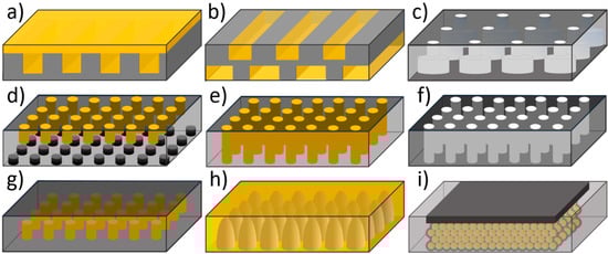
Figure 7. Examples of PC structures in the active layer: (a) 1D grating based on [123]; (b) double 1D grating based on [11]; (c) double layer of 2D PCs based on [122]; (d) double 2D PCs based on [110]; (e) 2D lattice of cylinders based on [117]; (f) 2D lattice of air cylinders based on [7][121]; (g) 2D PCs based on [118]; (h) lattice of nanocones based on [125]; (i) inverse opal based on [119].
3.4.1. 1D Photonic Crystal
1D PCs were theoretically and experimentally considered by Duche et al. [11] to enhance absorption in the active layer in organic solar cells. Their structure consisted of two layers with 1D gratings (Figure 7b). One of them was the active layer made of a blend of PCBM ([6][6]-phenyl-C61-butyric acid methyl ester) and one of the polymers: P3HT (poly-3-hexylthiophe’ne) with an energy band gap Eg~1.88 eV or TDPTD (poly(3-(2-methyl-2-hexyl-carboxylate) thiophene-co-thiophene)) with Eg~1.83 eV. Due to slow photons, they demonstrated photonic absorption gains for the integrated spectra on an 8° incident cone, 3.36% and 15.67% for P3HT:PCBM and TDPTD:PCBM, respectively [11]. Merabti et al. [127] theoretically explored the feasibility of 1D PC grating in the active layer of an a-Si:H-based photovoltaic cell. This structure led to more significant electro-optical gains thanks to the interference effects and coupling of incident light with slow Bloch modes.
3.4.2. 2D Photonic Crystal
2D structures have been the most often chosen PCs in designing solar cells for absorption enhancement.
Mallick et al. [122] restructured the active layer in ultrathin c-Si solar cells by patterning a 400 nm-thick c-Si layer into a double-layer PC with holes (Figure 7c). The holes in the upper layer had a smaller radius than those in the lower layer. This results in an enhancement of the maximum achievable photocurrent density from 7.1 mA/cm2 for an unstructured film to 21.8 mA/cm2 for a structured one, approaching the Yablonovitch light-trapping limit of 26.5 mA/cm2 for the same volume of active material. De Zoysa et al. [110][120] discussed enhancing broadband light absorption in the wavelength range of 600–1000 nm by utilizing multiple large-area resonant modes at the band edge of a PC in the case of ultrathin μc-Si film (Figure 7d). They achieved a high active-area current density of 22.6 mA cm−2 and obtained an active-area efficiency of >9.1% using a square-lattice 2D PC. Gomard’s team [7] studied 2D PCs for absorption enhancement in a-Si:H thin film. Their 100 nm-thick active material, patterned with a lattice of holes with squared symmetry, reached a high absorption of the incident light despite thickness below the diffusion length of the minority carriers [7]. Another proposal for improved light trapping in Si was presented in [129]. The approach was based on the quasi-resonant absorption of photons in a tandem arrangement of partially disordered photonic crystal plates separated by a nanoscale gap. This construction made it possible to surpass the Lambertian limit.
2D PC structures have also been implemented in organic solar cells [118][123][124][131][132]. Tumbleston et al. [123][124][132] attempted to enhance absorption in the active layer of organic solar cells by designing them in a photonic crystal structure: square posts with 395 nm 2D square periodicity and channels with 400 nm 1D periodicity. The research of Tumbleston’s team [123][131][132] on photonic crystal photoactive layers resulted in an increase in absorption by ~17% over the entire spectral range due to band edge excitation of quasi-guided modes [124]. The proposed active layer consisted of the poly-3-hexylthiophene/[6][6]-phenyl-C61-butyric acid methyl ester (P3HT:PCBM) bulk heterojunction blend and a porous form of low index of refraction (~1.4) conducting nanocrystalline zinc oxide (nc-ZnO). Additionally, PC geometry created excitons closer to the P3HT:PCBM exit interfaces [123]. Thus, free carriers might be more suited to escape from the photoactive blend, enhancing electrical performance readily. Another way of implementing 2D PCs in organic SCs was presented in [118] (Figure 7g). The author theoretically designed semitransparent organic solar cells with 2D photonic crystals inside the active layer, which was composed of two fullerene materials. She also concluded that PTB7-Th:PC71BM could be a better choice as an active layer than the P3HT:PCBM [118].
The improvement of absorption due to coupling incident light into quasi-guided modes has been investigated by Dottermusch et al. [125] in CuInSe (CIS) nanocrystalline-based solar cells. The 2D photonic structure was in the form of photoresist polymer nanocones of half-ellipsoidal shape arranged in a square lattice and embedded into a layer of CIS nanocrystals (Figure 7h). It resulted in absorption enhancement of only 3–7% because the low refractive index of the CIS nanocrystals was the main limiting factor that led to a restricted number of quasi-guided modes [125].
Another group of solar cells where an active layer was designed in the 2D PC were perovskite SCs [117][121][133]. The PC structure examined in [121] comprised air holes arranged into a hexagonal lattice (Figure 7f) in perovskite MAPbI3. The absorption enhancement was approximately 44% better than planar material [121]. A tetragonal lattice of indium arsenide (InAs) cylinders in the absorption layer of methylamine lead iodide (CH3NH3PbI3, MAPbI3) (Figure 7e) was presented in [117]. Implementing a photonic structure increased absorption efficiency up to 82.5% in the wide wavelength range of 400–1200 nm. This is much higher than the absorption layer without the PC structure. In addition, the absorption layer with photonic crystal presented a stable absorption efficiency of 80% in the wide incident range of 0–80°.
3.4.3. 3D Photonic Crystal
The only 3D structure of PC considered so far for the active layer of solar cells is inverse opal [115][116][119][130] (Figure 7i). It has been used in dye- and quantum dots-sensitized solar cells. Already in 2003, Nishimura et al. [112] noticed a ~26% increase in the short circuit photocurrent efficiency across the visible spectrum (400–750 nm) by coupling a photonic crystal to a dye-sensitized nanocrystalline TiO2 photoelectrode.
Mihi and Miguez [115] observed absorption enhancement in various spectral regions depending on the size of the spheres and, thus, depending on the position of the PBG relative to the absorption edge while studying dye-sensitized nc-TiO2 inverse opal. This effect occurs for the photonic band gap’s red and blue edges. However, they concluded that better outcomes were achieved in the structure consisting of PCs and a bulk layer of absorbing material than in the photonic crystals only. The absorption enhancement occurs in resonant modes localized within the absorbing coating rather than in the photonic crystals. The latter plays the role of a mirror operating through coherent scattering. This was confirmed experimentally by Lee et al. [119]. Bayram and Halaoui [116] examined solar cells based on quantum-confined CdSe-sensitized TiO2 photonic crystals to amplify solar energy conversion. They observed an almost sevenfold amplification of the photon-to-current conversion efficiency for the examined inverse opal structure compared to a nanocrystalline TiO2 with similar CdSe sensitization [116]. The authors attributed this enhancement to a blue-edge slow photon effect due to overlapping the photonic band gap at 700 nm with the CdSe absorption edge (600–650 nm). The quantum dot Q-CdTe/Se layer-sensitized TiO2 inverse opal featured a four-fold enhancement factor of the photon-to-current conversion [130].
3.5. Additional Light Management Layer
Photonic crystals have also been introduced into SCs as light management layers [134][135][136]. As mentioned in the previous section, in dye-sensitized solar cells, better effects were achieved when colloidal PCs were used as an additional layer rather than the active one alone [115]. In [137], an additional multilayer colloidal structure composed of spheres with different diameters led to light harvesting enhancement of approximately 60% compared to standard dye-sensitized solar cells due to the mirror behavior of the colloidal superlattice.
Buencuerpo et al. [135][138] simulated an ultrathin GaAs solar cell including additional PC layers: only on the front side, only on the back side, and on both the front and back sides of the active layer. The front layer was composed of TiO2 cylinders arranged in a square lattice inside an ARC of MgF2 when used alone or arranged in two displaced square lattices combined with the back PC layer. The latter was made of AlGaAs cylinders arranged in a square lattice inside a SiO2 spacer.
Producing periodic nanostructures is challenging and expensive; thus, the proposition of less demanding quasi-random photonic structures (e.g., disordered structures with a precisely defined reciprocal space distribution of spatial frequencies) has appeared [136][139]. An additional layer built into the back of GaAs solar cells led to a 10% relative improvement [136].
3.6. Radiation Cooler (RC)
An inherent effect of the work of solar cells is their heating. This undesirable effect adversely affects the efficiency of solar-to-electricity conversion and the lifetime of photovoltaic panels. The efficiencies of different PV technologies decrease with temperature, e.g., the efficiency of crystalline Si modules decreases at a rate of 0.45%/°C [140][141]. In the long run, high temperature activates and accelerates such unfavorable processes as contact corrosion and polymer degradation. As a result, in hot climates, the power degradation of crystalline Si photovoltaic modules progresses at approximately 1.8% per year, which is almost nine times faster than modules installed in cold climates (approximately 0.2% per year) [142]. In hot climates, the module lifetime was less than 15 years, well below the standard 25-year warranty for solar panels. Lowering the temperature of the cells is, therefore, a key factor in improving their efficiency and lifetime, which is vital in producing electronic waste. It is critically important to develop effective, practical, and preferably passive cooling methods to reduce the operating temperature of photovoltaic (PV) modules. This can be achieved by using the radiative cooling effect (RC), i.e., the process of heat loss by thermal radiation that can pass through the atmosphere into outer space. It is possible in the so-called atmospheric transparency window, i.e., in the 8–13 µm wavelength range. Materials that can absorb energy and radiate it in those wavelengths exhibit a strong cooling effect. However, it must be considered that for photovoltaic applications, lowering the operating temperature by RC is only viable if sunlight absorption can be maintained simultaneously.
Commercial solar cells are usually encapsulated with polymer or glass covers [143] and have a glass cover on top [144]. This glass protects delicate elements of PV modules from dirt, moisture, and mechanical damage. This glass is also a cooling element due to its inherent RC capability. Even though glass is already highly emissive in the IR region, it is still imperfect. Therefore, efforts are underway to produce materials that could support or replace glass in heat dissipation and be used to cool photovoltaic panels. Nanostructured materials, especially photonic crystals, may play an essential role. The thermal emission of photonic crystals was noticed and studied very early. Enhancement and suppression of thermal emission of radiation have been theoretically and experimentally demonstrated, among others, in 1D [145][146][147][148], 2D [149][150][151][152][153], and 3D [154][155][156][157][158][159][160] photonic crystals, as well as in structures composed of 2D and 1D photonic crystals [161]. However, not all of them met the requirements for solar cell radiative coolers, e.g., because of the significant reflection of incident solar irradiance.
Gao et al. [162] argue that “an optimised radiative cooler should exhibit the following characteristics: (1) its substrate should not be constrained (i.e., the cooler can be manufactured to be rigid or flexible), (2) it should be capable of large-area manufacture, (3) have photonic crystal structures with wide emissive angles, (4) be inexpensive, (5) have a near-ideal emittance profile, and (6) be capable of reducing the operating temperature of solar cells. However, manufacturing a radiative cooler with the above characteristics is still challenging”.
Zhao et al. [163] proposed and analyzed a photonic structure composed of 1D and 2D photonic crystals that selectively reflect solar radiation and actively radiate heat to outer space while maintaining its solar transmission in the PV conversion band (0.3–1.1 μm). The 1D photonic crystal forms a multilayer stack of alternating SiO2 and TiO2 layers (30 layers in total) deposited on a single layer of MgF2. On top of this stack is placed a 2D photonic crystal which, like in [164], is a square lattice (period = 6 μm) of air rods (diameter = 5 μm, depth = 10 μm) etched into a uniform layer of silica (thickness = 500 μm).
The structure designed in this way is characterized by close-to-unity transmission and, thus, the low reflection of sunlight in the range of 0.3–1.1 μm. However, in the entire range of mid-infrared waves and the atmospheric transmission window, the emissivity/absorptivity of this structure is very high. Additionally, the structure is a good reflector for near-infrared radiation above 1.1 μm (see Figure 4 in [163]). In their thermal simulation, Zhao et al., like Zhu et al. in [153], also considered other nonradiative heat dissipation mechanisms. The proposed photonic structure on top of the solar cell lowers its operating temperature by 10 °C. It is 7 °C lower than achieved for SCs with a glass coating on top and only 1 °C higher than SCs with an ideal heat emitter.
Gao et al. [162] made and experimentally tested the effectiveness of a photonic structure formed by a square lattice of 2D truncated cones deposited on a polyethylene terephthalate (PET) substrate. They designed the optimal structure using numerical simulations for various shapes, sizes, and periodicity to maximize emittance in the atmospheric transparency window. For the fabrication, Gao et al. used the UV nanoimprint method on a UV-curable adhesive (UVA) [162], which is much more economical than, for example, photolithography. The rooftop measurement showed that the photonic structure reduced the temperature of the underlying silicon wafer by approximately 1.2 °C. A much better effect was achieved when an additional layer of Ag was applied to the PET substrate. This layer significantly reflected solar radiation, which helped reduce the temperature by 7.7 °C but was not beneficial for the efficiency of solar cells.
A similar 2D structure in the form of SiO2 pillars was examined by Long et al. in [165]. They theoretically concluded that in extreme cases, for no convective heat coefficient (no wind), the designed structure should reduce the temperature of the solar cell by 16 °C. Simultaneously, they obtained a reduction of 2 °C compared with the bare structure during the rooftop measurement.
Unlike previous structures, Silva-Oelker and Jaramillo-Fernandez [166] numerically analyzed 2D structures based on hemispheres and a flat surface placed on a silicon photovoltaic cell. Considering different geometrical parameters, they determined maximum power improvements of 18.1% and 19.7% when using soda-lime and polydimethylsiloxane (PDMS) hemispheres, respectively, and a temperature reduction of 4 °C compared to a glass encapsulated solar cell.
The radiative cooler proposed by An et al. [56] integrates a multilayer thin-film stack and a SiO2 grating. They performed a comparable theoretical study on the performance parameters of the SCs with and without the radiative cooler. In this way, they showed that the SC temperature can be reduced by over 10 °C and the absolute power conversion efficiency (PCE) can be increased by 0.45% by employing the photonic radiative cooler. Zhao et al. [167] performed an outdoor experiment with silica micrograting as a cooler. Their structure fabricated through the etching process has a periodicity of 7 μm, a duty ratio of 0.2, and a vertical depth of 10 μm. The grating was highly transparent to sunlight and reduced the temperature of the commercial silicon cell by over 3.6 °C after adding it on top. Additionally, the proposed silica grating reinforced the light-trapping effect of the solar cell.
The 3D photonic crystal with an opal structure also has good cooling properties. [168]. It should be emphasized that opals are easy to produce and cheap. Besides cooling effects, applying opals with different sphere sizes caused the desired colorization. Kim et al. [168] implemented self-assembled silica opals on a silicon (Si) wafer. Daytime radiative cooling of the c-Si by as much as 13 °C while maintaining the nonabsorbing colorization is achieved through colloidal suspension coating.
3.7. Electron Transport Layer
ETLs are conductive scaffolds coated with perovskite, which extract electrons from perovskite and deliver them onto a transparent electrode, blocking charge recombination [169][170] and eliminating the space charge [52]. Mesoporous TiO2 [170], ZnO [52][132], and PFN [52][78] are the materials applied in ETLs. The electron transport layer’s microstructure plays an important role that invariably affects the perovskite infiltration, light trapping, harvesting, and charge injection, transportation, and collection at the ETL/perovskite interfaces. Highly oriented arrays of nanorods, nanowires, and nanotubes have been widely used as ETLs in PSCs [171][172][173].
Kim et al. [58] examined a layer with a TiO2 hemisphere structure which was prepared using the nanoimprint technique. By controlling the dimension of the hemispheres, they concluded that the 1400 nm-sized hemisphere pattern using 1600 nm polystyrene beads provided the highest light-utilization efficiency among those in the visible range. In addition, the recombination rate of the electron transport layer was also decreased. As a result, the power conversion efficiency of perovskite solar cells was improved from 10.5 to 15.2%.
Another ETL monolayer structure was reported in [174]. It was a well-organized monolayer SnO2 inverse opal. Its periodic structure exhibited an optical coupling phenomenon, enhancing the perovskite layer’s light absorption. Furthermore, the well-organized structure with appropriate pore size triggered the confined crystallization of perovskite films and optimized the interface of SnO2/perovskites, suppressing the interfacial electron–hole recombination. As a result, the power conversion efficiency of mesoporous perovskite solar cells fabricated was boosted from 19.63% for the control device with a layer of mesoporous SnO2 to 22.01% for devices with a SnO2 inverse opal layer as an ETL.
Zheng et al. [175] presented a dual porous TiO2 ETL for carbon cathode-based perovskite solar cells. This layer was constructed by spin-coating on a polystyrene sphere template. It was demonstrated that the unique structure could enhance the light harvesting efficiency via scattering and promote the crystallinity of the supported perovskite film and the perovskite/TiO2 interface, thereby improving the performance of the carbon-perovskite solar cell. The authors achieved 9.81% power conversion efficiency.
References
- Guo, K.W. Green nanotechnology of trends in future energy: A review. Int. J. Energy Res. 2011, 36, 1–17.
- Luque, A.; Hegedus, S. (Eds.) . Handbook of Photovoltaic Science and Engineering; John Wiley & Sons: Hoboken, NJ, USA, 2011.
- Pastuszak, J.; Węgierek, P. Photovoltaic cell generations and current research directions for their development. Materials 2022, 15, 5542.
- Green, M.A.; Dunlop, E.D.; Yoshita, M.; Kopidakis, N.; Bothe, K.; Siefer, G.; Hao, X. Solar cell efficiency tables (version 62). Prog. Photovolt. Res. Appl. 2023, 31, 651–663.
- Marques Lameirinhas, R.A.; Torres, J.P.N.; de Melo Cunha, J.P. A Photovoltaic Technology Review: History, Fundamentals and Applications. Energies 2022, 15, 1823.
- Jiménez-Solano, A.; Delgado-Sánchez, J.M.; Calvo, M.E.; Miranda-Muñoz, J.M.; Lozano, G.; Sancho, D.; Sánchez-Cortezón, E.; Míguez, H. Design and realization of transparent solar modules based on luminescent solar concentrators integrating nanostructured photonic crystals. Prog. Photovolt. Res. Appl. 2015, 23, 1785–1792.
- Gomard, G.; Drouard, E.; Letartre, X.; Meng, X.; Kaminski, A.; Fave, A.; Lemiti, M.; Garcia-Caurel, E.; Seassal, C. Two-dimensional photonic crystal for absorption enhancement in hydrogenated amorphous silicon thin film solar cells. J. Appl. Phys. 2010, 108, 123102.
- Meng, X.; Depauw, V.; Gomard, G.; El Daif, O.; Trompoukis, C.; Drouard, E.; Jamois, C.; Fave, A.; Dross, F.; Gordon, I.; et al. Design, fabrication and optical characterization of photonic crystal assisted thin film monocrystalline-silicon solar cells. Opt. Express 2012, 20, A465–A475.
- Guldin, S.; Huttner, S.; Kolle, M.; Welland, M.E.; Muller-Buschbaum, P.; Friend, R.H.; Steiner, U.; Tétreault, N. Dye-sensitized solar cell based on a three-dimensional photonic crystal. Nano Lett. 2010, 10, 2303–2309.
- Diguna, L.J.; Shen, Q.; Kobayashi, J.; Toyoda, T. High efficiency of CdSe quantum-dot-sensitized TiO2 inverse opal solar cells. Appl. Phys. Lett. 2007, 91, 023116.
- Duché, D.; Masclaux, C.; Le Rouzo, J.; Gourgon, C. Photonic crystals for improving light absorption in organic solar cells. J. Appl. Phys. 2015, 117, 053108.
- Choi, D.H.; Nam, S.K.; Jung, K.; Moon, J.H. 2D photonic crystal nanodisk array as electron transport layer for highly efficient perovskite solar cells. Nano Energy 2019, 56, 365–372.
- Ramautarsingh, B.D.A.; O’Brien, P.G.; Flood, A.G.; Kherani, N.P. Quantum efficiency enhancement in multi-junction solar cells with spectrally selective and conducting 1D photonic crystals. J. Mater. Chem. C 2016, 4, 9276–9286.
- Waketola, A.G.; Hone, F.G.; Mola, G.T.; Oseni, S.O.; Ogutu, H.; Tegegne, N.A. Hybrid silver/silver-oxide nanoparticles doped hole transport layer for efficient photon harvesting in organic solar cells. Appl. Phys. A 2023, 129, 96.
- Yang, L.; Li, L.; Kong, W.; Zhen, Z. Metal nanoparticles influence on light absorbed power of thin-film solar cell with periodic structure. Optik 2013, 124, 1921–1925.
- Muchuweni, E.; Mombeshora, E.T.; Martincigh, B.S.; Nyamori, V.O. Recent applications of carbon nanotubes in organic solar cells. Front. Chem. 2022, 9, 733552.
- Levitsky, I.A. Hybrid solar cells based on carbon nanotubes and Nanoporous silicon . IEEE Nanotechnol. Mag. 2010, 4, 24–25.
- Najafi, L.; Taheri, B.; Martin-Garcia, B.; Bellani, S.; Di Girolamo, D.; Agresti, A.; Oropesa-Nuñez, R.; Pescetelli, S.; Vesce, L.; Calabrò, E.; et al. MoS2 quantum dot/graphene hybrids for advanced interface engineering of a CH3NH3PbI3 perovskite solar cell with an efficiency of over 20%. ACS Nano 2018, 12, 10736–10754.
- Brunetti, F.; Ulisse, G.; Dianetti, M.; Susanna, G.; Innaccone, G.; Fiori, G.; Martin, O.; Neumaier, D.; Puicervert, R.; Lordan, D.; et al. Doped and textured graphene as electrode for organic solar cells. In Proceedings of the 2015 IEEE 15th International Conference on Nanotechnology (IEEE-NANO), Rome, Italy, 27–30 July 2015; pp. 560–563.
- Wang, K.X.; Yu, Z.; Liu, V.; Raman, A.; Cui, Y.; Fan, S. Light trapping in photonic crystals. Energy Environ. Sci. 2014, 7, 2725–2738.
- Sakoda, K. Optical Properties of Photonic Crystals; Springer Series in Optical Sciences: Berlin/Heidelberg, Germany, 2005; p. 80.
- Garcia-Adeva, A. Band gap atlas for photonic crystals having the symmetry of the kagome and pyrochlore lattices. New J. Phys. 2006, 8, 86.
- Rybin, M.V.; Shishkin, I.I.; Samusev, K.B.; Belov, P.A.; Kivshar, Y.S.; Kiyan, R.V.; Chichkov, B.N.; Limonov, M.F. Band structure of photonic crystals fabricated by two-photon polymerization. Crystals 2015, 5, 61–73.
- Available online: http://www.filmetrics.com/reflectance-calculator (accessed on 24 January 2024).
- Johnson, S.G.; Fan, S.; Villeneuve, P.R.; Joannopoulos, J.D.; Kolodziejski, L.A. Guided modes in photonic crystal slabs. Phys. Rev. B 1999, 60, 5751.
- Kok, A.; Geluk, E.; Sander-Jochem, M.; van der Tol, J.J.G.M.; Oei, Y.; Smit, M. Two-dimensional photonic crystals based on In P rods. In Proceedings of the IEEE/LEOS Symposium, Mons, Belgium; 2005; pp. 273–276.
- Krauss, T.F. Planar photonic crystal waveguide devices for integrated optics. Phys. Status Solidi 2003, 197, 688–702.
- Rong, B.; Salemink, H.W.; Roeling, E.M.; van der Heijden, R.; Karouta, F.; van der Drift, E. Fabrication of two dimensional GaN nanophotonic crystals (31). J. Vac. Sci. Technol. B 2007, 25, 2632–2636.
- van der Heijden, R.; van der Drift, E.W.J.M.; Geluk, E.J.; van der Heijden, R.W.; Karouta, F.; Nouwens, P.A.M.; Oei, Y.S.; dr Vries, T.; Salemink, H.W.M. Deep dry etching process development for InP-based photonic crystals. In Proceedings of the IEEE/LEOS, Tucson, AZ, USA, 27–28 October 2003; pp. 257–260.
- El-Kallassi, P.; Ferrini, R.; Zuppiroli, L.; Le Thomas, N.; Houdré, R.; Berrier, A.; Anand, S.; Talneau, A. Optical tuning of planar photonic crystals infiltrated with organic molecules. J. Opt. Soc. Am. B 2007, 24, 2165–2171.
- Zijlstra, T.; van der Drift, E.W.J.M.; de Dood, M.J.A.; Snoeks, E.; Polman, A. Fabrication of two-dimensional photonic crystal waveguides for 1.5 μm in silicon by deep anisotropic dry etching. J. Vac. Sci. Technol. B 1999, 17, 2734–2739.
- Tada, T.; Poborchii, V.V.; Kanayama, T. Channel waveguides fabricated in 2D photonic crystals of Si nanopillars. Microelectron. Eng. 2002, 63, 259–265.
- Assefa, S.; Rakich, P.T.; Bienstman, P.; Johnson, S.G.; Petrich, G.S.; Joannopoulos, J.D.; Kolodziejski, L.A.; Ippen, E.P.; Smith, H.I. Guiding 1.5 μm light in photonic crystals based on dielectric rods. Appl. Phys. Lett. 2004, 85, 6110–6112.
- Tokushima, M.; Yamada, H.; Arakawa, Y. 1.5-μm-wavelength light guiding in waveguides in square-lattice-of-rod photonic crystal slab. Appl. Phys. Lett. 2004, 84, 4298–4300.
- Kraeh, C.; Popsecu, A.; Schieber, M.; Hedler, H.; Bieniek, T.; Wielgoszewski, G.; Moczała, M.; Finley, J. Fabrication of high aspect ratio microtube arrays for 2D photonic crystals. Mater. Res. Express 2014, 1, 026201.
- Kraeh, C.; Martinez-Hurtado, J.L.; Zeitlmair, M.; Popescu, A.; Hedler, H.; Finley, J.J. Strong transmittance above the light line in mid-infrared two-dimensional photonic crystals. J. Appl. Phys. 2015, 117, 223101.
- Baba, T.; Matsuzaki, T. Theoretical calculation of photonic gap in semiconductor 2-dimensional photonic crystals with various shapes of optical atoms. Jpn. J. Appl. Phys. 1995, 34, 4496–4498.
- Broeng, J.; Mogilevstev, D.; Barkou, S.E.; Bjarklev, A. Photonic crystal fibers: A new class of optical waveguides. Opt. Fiber Technol. 1999, 5, 305–330.
- Ho, K.M.; Chan, C.T.; Soukoulis, C.M. Existence of a photonic gap in periodic dielectric structures. Phys. Rev. Lett. 1990, 65, 3152.
- Ho, K.M.; Chan, C.T.; Soukoulis, C.M.; Biswas, R.; Sigalas, M. Photonic band gaps in three dimensions: New layer-by-layer periodic structures. Solid State Commun. 1994, 89, 413–416.
- Joannopoulos, J.D.; Johnson, S.G.; Winn, J.N.; Meade, R.D. Photonic Crystals: Molding the Flow of Light, 2nd ed.; Princeton University Press: Singapore, 2008.
- Notomi, M. Theory of light propagation in strongly modulated photonic crystals: Refractionlike behavior in the vicinity of the photonic band gap. Phys. Rev. B 2000, 62, 10696.
- Meade, R.D.; Brommer, K.D.; Rappe, A.M.; Joannopoulos, J.D. Existence of a photonic band gap in two dimensions. Appl. Phys. Lett. 1992, 61, 495–497.
- Busch, K.; John, S. Photonic band gap formation in certain self-organizing systems. Phys. Rev. E 1998, 58, 3896.
- Kępińska, M.; Starczewska, A.; Duka, P.; Nowak, M.; Szperlich, P. Optical properties of SbSI photonic crystals. Acta Phys. Pol. A 2014, 126, 1115–1117.
- Starczewska, A.; Szperlich, P.; Nowak, M.; Bednarczyk, I.; Bodzenta, J.; Szala, J. Fabrication of SbSI Photonic Crystals. Acta Phys. Pol. A 2014, 126, 1118–1120.
- Bao, Y.; Wang, D.; Hui, W.; Gu, L.; Chao, L.; Song, L. Honeycomb-type TiO2 films toward a high tolerance to optical paths for perovskite solar cells. Chem. Sus. Chem. 2023, 16, e202201749.
- Bhattacharya, S.; John, S. Designing high-efficiency thin silicon solar cells using parabolic-pore photonic crystals. Phys. Rev. Appl. 2018, 9, 044009.
- Chaouachi, A.; Chtourou, R.; M’nif, A.; Hamzaoui, A.H. Optimal enhancement in conversion efficiency of crystalline Si solar cells using inverse opal photonic crystals as back reflectors. J. Opt. 2015, 17, 045106.
- Jain, S.K.; Janyani, V.; Gupta, N.D. Optical Studies of Cadmium Telluride based Solar Cell using Photonic Crystal as a back Reflector. In Proceedings of the 2022 Workshop on Recent Advances in Photonics (WRAP), Mumbai, India, 4–6 March 2022; pp. 1–2.
- Çetinkaya, Ç.; Çokduygulular, E.; Kınacı, B.; Güzelçimen, F.; Özen, Y.; Sönmez, N.A.; Özçelik, S. Highly improved light harvesting and photovoltaic performance in CdTe solar cell with functional designed 1D-photonic crystal via light management engineering. Sci. Rep. 2022, 12, 11245.
- Zheng, W.; Luo, X.; Zhang, Y.; Ye, C.; Qin, A.; Cao, Y.; Hou, L. Efficient low-cost all-flexible microcavity semitransparent polymer solar cells enabled by polymer flexible one-dimensional photonic crystals. ACS Appl. Mater. Interfaces 2020, 12, 23190–23198.
- Fatehi, N.; Olyaee, S.; Seifouri, M.; Parandin, F. Design of a high-efficiency perovskite solar cell based on photonic crystal in the absorption layer. Opt. Quantum Electron. 2024, 56, 386.
- Niu, H.; Shao, J.; Xie, Y.; Ye, T.; Li, T.; Luo, S.; Yao, X. Application of carbon nanosphere templates for preparation of inverse opal photonic crystals in dye-sensitized solar cells. Phys. Status Solidi 2023, 220, 2300221.
- Perrakis, G.; Tasolamprou, A.C.; Kenanakis, G.; Economou, E.N.; Tzortzakis, S.; Kafesaki, M. Submicron organic–inorganic hybrid radiative cooling coatings for stable, ultrathin, and lightweight solar cells. ACS Photon. 2022, 9, 1327–1337.
- An, Y.; Sheng, C.; Li, X. Radiative cooling of solar cells: Opto-electro-thermal physics and modeling. Nanoscale 2019, 11, 17073–17083.
- Chen, X.; Yang, S.; Zheng, Y.C.; Chen, Y.; Hou, Y.; Yang, X.H.; Yang, H.G. Multifunctional inverse opal-like TiO2 electron transport layer for efficient hybrid perovskite solar cells. Adv. Sci. 2015, 2, 1500105.
- Kim, D.I.; Lee, J.W.; Jeong, R.H.; Yu, J.H.; Yang, J.W.; Nam, S.H.; Boo, J.H. Enhancing the optical properties using hemisphere TiO2 photonic crystal as the electron acceptor for perovskite solar cell. Appl. Surf. Sci. 2019, 487, 409–415.
- Almawgani, A.H.; Medhat, M.; Mehaney, A.; Ali, G.A.; Irfan, M.; Elsayed, H.A. One-dimensional metamaterial photonic crystals comprising gyroidal and hyperbolic layers as an angle-insensitive reflector for energy applications in IR regions. Eur. Phys. J. Plus 2023, 138, 483.
- Kumar, M.; Pandian, T.B.; Sreekiran, E.; Narayanan, S. Benefit of dual layer silicon nitride anti-reflection coating. In Proceedings of the Conference Record of the Thirty-First IEEE Photovoltaic Specialists Conference, Lake Buena Vista, FL, USA, 3–7 January 2005.
- Green, M.A.; Blakers, A.W.; Jiqun, S.; Keller, E.M.; Wenham, S.R. High-efficiency silicon solar cells. IEEE Trans. Electron Devices 1984, 31, 679–683.
- Sayed, H.; Matar, Z.S.; Al-Dossari, M.; Amin, A.F.; Abd El-Gawaad, N.S.; Aly, A.H. The design and optimization of an anti-reflection coating and an intermediate reflective layer to enhance tandem solar cell photons capture. Crystals 2022, 12, 57.
- Fedawy, M.; Ali, S.M.; Abdolkader, T. Efficiency Enhancement of GaAs Solar Cell using Si3N4 Anti-reflection Coating. J. Adv. Res. Mater. Sci. 2018, 42, 1–7.
- Sayed, H.; Al-Dossari, M.; Ismail, M.A.; Abd El-Gawaad, N.S.; Aly, A.H. Theoretical Analysis of Optical Properties for Amorphous Silicon Solar Cells with Adding Anti-Reflective Coating Photonic Crystals. Photonics 2022, 9, 813.
- Womack, G.; Kaminski, P.M.; Abbas, A.; Isbilir, K.; Gottschalg, R.; Walls, J.M. Performance and durability of broadband antireflection coatings for thin film CdTe solar cells. J. Vac. Sci. Technol. A 2017, 35, 021201.
- Matsuoka, Y.; Mathonnèire, S.; Peters, S.; Masselink, W.T. Broadband multilayer anti-reflection coating for mid-infrared range from 7 μm to 12 μm. Appl. Opt. 2018, 57, 1645–1649.
- Aly, A.H.; Sayed, H. Photonic band gap materials and monolayer solar cell. Surf. Rev. Lett. 2018, 25, 1850103.
- Aly, A.H.; Sayed, H.; Elsayed, H.A. Development of the monolayer silicon solar cell based on photonic crystals. Silicon 2019, 11, 1377–1382.
- Bennet, P.; Juillet, P.; Ibrahim, S.; Berthier, V.; Barry, M.A.; Réveret, F.; Bousquet, A.; Teytaud, O.; Centeno, E.; Moreau, A. Analysis and fabrication of antireflective coating for photovoltaics based on a photonic-crystal concept and generated by evolutionary optimization. Phys. Rev. B 2021, 103, 125135.
- Sankar, K.; Manoharan, R.; Saif, S.; Rose, T.P. An optimum design of one dimensional photonic crystal for solar cell applications. In IOP Conference Series: Materials Science and Engineering; IOP Publishing: Bristol, UK, 2022; Volume 1219, p. 012047.
- Hung, Y.-J.; San-Liang, L.; Coldren, L.A. Deep and tapered silicon photonic crystals for achieving anti-reflection and enhanced absorption. Opt. Express 2010, 18, 6841–6852.
- Domínguez, S.; Cornago, I.; García, O.; Ezquer, M.; Rodríguez, M.J.; Lagunas, A.R.; Pérez-Conde, J.; Bravo, J. Design, optimization and fabrication of 2D photonic crystals for solar cells. Photon. Nan. Fundam. Appl. 2013, 11, 29–36.
- Przybylski, D.; Patela, S. Modelling of a two-dimensional photonic crystal as an anti-reflection coating for optoelectronic applications. Opto-Electron. Rev. 2019, 27, 79–89.
- Branham, M.S.; Hsu, W.C.; Yerci, S.; Loomis, J.; Boriskina, S.V.; Hoard, B.R.; Han, S.E.; Chen, G. 15.7% efficient 10-μm-thick crystalline silicon solar cells using periodic nanostructures. Adv. Mater. 2015, 27, 2182–2188.
- Kuang, P.; Eyderman, S.; Hsieh, M.L.; Post, A.; John, S.; Lin, S.Y. Achieving an accurate surface profile of a photonic crystal for near-unity solar absorption in a super thin-film architecture. ACS Nano 2016, 10, 6116–6124.
- Gupta, N.D.; Janyani, V. Design and analysis of light trapping in thin film GaAs solar cells using 2-D photonic crystal structures at front surface. IEEE J. Quantum Electron. 2017, 53, 1–9.
- Bhattacharya, S.; Baydoun, I.; Lin, M.; John, S. Towards 30% power conversion efficiency in thin-silicon photonic-crystal solar cells. Phys. Rev. Appl. 2019, 11, 014005.
- Liu, W.; Hailing, M.; Annika, W. Advance in photonic crystal solar cells. Renew. Sustain. Energy Rev. 2019, 116, 109436.
- Li, T. Enhancement of light absorption in thin film silicon solar cells with light traping. Chin. J. Lumin. 2016, 37, 816–822.
- Kuang, P.; Bhattacharya, S.; Hsieh, M.L.; John, S.; Lin, S.Y. Photonic crystals with a continuous, Gaussian-type surface profile for near-perfect light trapping. J. Nanophotonics 2018, 12, 026011.
- Bhattacharya, S.; John, S. Photonic crystal light trapping: Beyond 30% conversion efficiency for silicon photovoltaics. APL Photon. 2020, 5, 020902.
- Yang, L.; Liu, Y.; Wang, Y.; Chen, W.; Chen, Q.; Wu, J.; Kuznetsov, A.; Du, X. 18.87%-efficient inverted pyramid structured silicon solar cell by one-step Cu-assisted texturization technique. Sol. Energy Mater. Sol. Cells 2017, 166, 121–126.
- Almenabawy, S.M.; Zhang, Y.; Prinja, R.; Sharma, G.; Kherani, N.P. Design, Fabrication and Optical Characterization of Photonic Crystal Patterned Ultra-Thin Silicon. In Proceedings of the 2020 47th IEEE Photovoltaic Specialists Conference (PVSC), Calgary, AB, Canada, 15 June–21 August 2020; pp. 2304–2307.
- Almenabawy, S.; Zhang, Y.; Flood, A.; Prinja, R.; Kherani, N.P. Nanometer-mesa inverted-pyramid photonic crystals for thin silicon solar cells. ACS Appl. Energy Mater. 2022, 5, 13808–13816.
- Ishizaki, K.; Motohira, A.; De Zoysa, M.; Tanaka, Y.; Umeda, T.; Noda, S. Microcrystalline-silicon solar cells with photonic crystals on the top surface. IEEE J. Photovolt. 2017, 7, 950–956.
- Razzaq, A.; Depauw, V.; Cho, J.; Radhakrishnan, H.S.; Gordon, I.; Szlufcik, J.; Abdulraheem, Y.; Poortmans, J. Periodic inverse nanopyramid gratings for light management in silicon heterojunction devices and comparison with random pyramid texturing. Sol. Energy Mater. Sol. Cells 2020, 206, 110263.
- Razzaq, A.; Mayer, A.; Depauw, V.; Gordon, I.; Hajjiah, A.; Poortmans, J. Application of a genetic algorithm in four-terminal perovskite/crystalline-silicon tandem devices. IEEE J. Photovolt. 2020, 10, 1689–1700.
- Zhan, C.; Cai, J. The reflectivity of 1D+ 2D PC back reflector in thin-film solar cell. J. Opt. 2023, 52, 167–174.
- Hao, Y.; Sun, X.H.; Jiang, L.D.; Zhang, X.; Wang, G.L. Applications of Photonic Crystals in Solar Cells. Adv. Mater. Res. 2013, 760, 281–285.
- Hsieh, M.L.; Kaiser, A.; Bhattacharya, S.; John, S.; Lin, S.Y. Experimental demonstration of broadband solar absorption beyond the lambertian limit in certain thin silicon photonic crystals. Sci. Rep. 2020, 10, 11857.
- Korkmaz, V.; Etin, A.C. Optical visible wavelength region selective reflector design for photovoltaic cells using photonic crystal. Turk. J. Phys. 2017, 41, 491–497.
- Ingenito, A.; Isabella, O.; Zeman, M. Experimental demonstration of 4 n 2 classical absorption limit in nanotextured ultrathin solar cells with dielectric omnidirectional back reflector. ACS Photon. 2014, 1, 270–278.
- Yu, W.; Ruan, S.; Long, Y.; Shen, L.; Guo, W.; Chen, W. Light harvesting enhancement toward low IPCE region of semitransparent polymer solar cells via one-dimensional photonic crystal reflectors. Sol. Energy Mater. Sol. Cells 2014, 127, 27–32.
- Delgado-Sanchez, J.M.; Lillo-Bravo, I. Angular dependence of photonic crystal coupled to photovoltaic solar cell. Appl. Sci. 2020, 10, 1574.
- Saravanan, S.; Dubey, R.S. Performance enhancement of amorphous silicon solar cell using 1D photonic crystal as back reflector. Mater. Today Proc. 2022, 49, 2822–2825.
- Dubey, R.S.; Someswararao, M.V.; Saravanan, S. Photonic band gap analysis of 1D TiO2/SiO2 photonic crystals using plane wave method for thin film solar cell applications. In IOP Conference Series: Materials Science and Engineering; IOP Publishing: Bristol, UK, 2022; Volume 1263; p. 012007.
- Eghbali, R.; Khosroabadi, S.; Shokouhmand, A. A Novel Light trapping for high efficiency a-Si:H/μc-Si Micromorph tandem Solar Cells. Res. Sq. 2022.
- Basyooni, M.A.; Houimi, A.; Tihtih, M.; Zaki, S.E.; Boukhoubza, I.; Belaid, W.; En-nadir, R.; Ibrahim, J.E.F.M.; Attia, G.F. Boosting the efficiency of Cu2ZnSnS4 solar cells with VO2 phase transition photonic crystal. Opt. Mater. 2023, 138, 113717.
- Doghmosh, N.; Taya, S.A.; Upadhyay, A.; Olaimat, M.M.; Colak, I. Enhancement of optical visible wavelength region selective reflector for photovoltaic cell applications using a ternary photonic crystal. Optik 2021, 243, 167491.
- Zeng, L.; Yi, Y.; Hong, C.; Liu, J.; Feng, N.; Duan, X.; Kimerling, L.C.; Alamariu, B.A. Efficiency enhancement in Si solar cells by textured photonic crystal back reflector. Appl. Phys. Lett. 2006, 89, 111111.
- Zhou, D.; Biswas, R. Photonic crystal enhanced light-trapping in thin film solar cells. J. Appl. Phys. 2008, 103, 093102.
- Chen, P.; Hou, G.; Fan, Q.; Huang, Q.; Zhao, J.; Zhang, J.; Ni, J.; Zhang, X.; Zhao, Y. An efficient light trapping scheme based on textured conductive photonic crystal back reflector for performance improvement of amorphous silicon solar cells. Appl. Phys. Lett. 2014, 105, 073506.
- Biswas, R.; Bhattacharya, J.; Lewis, B.; Chakravarty, N.; Dalal, V. Enhanced nanocrystalline silicon solar cell with a photonic crystal back-reflector. Sol. Energy Mater. Sol. Cells 2010, 94, 2337–2342.
- Varghese, L.T.; Xuan, Y.; Niu, B.; Fan, L.; Bermel, P.; Qi, M. Enhanced Photon Management of Thin-Film Silicon Solar Cells Using Inverse Opal Photonic Crystals with 3D Photonic Bandgaps. Adv. Opt. Mater. 2013, 1, 692–698.
- Sundar, G.A.; Wilson, K.J. 1-D Magnetic photonic crystal as intermediate reflective layer in tandem solar cells. Hybrid Adv. 2022, 1, 100003.
- Bielawny, A.; Üpping, J.; Miclea, P.T.; Wehrspohn, R.B.; Rockstuhl, C.; Lederer, F.; Peters, M.; Steidl, L.; Zentel, R.; Lee, S.-M.; et al. 3D photonic crystal intermediate reflector for micromorph thin-film tandem solar cell. Phys. Status solidi 2008, 205, 2796–2810.
- O’Brien, P.G.; Chutinan, A.; Leong, K.; Kherani, N.P.; Ozin, G.A.; Zukotynski, S. Photonic crystal intermediate reflectors for micromorph solar cells: A comparative study. Opt. Express 2010, 18, 4478–4490.
- Amiri, I.S.; Yupapin, P.; Suseendran, G.; Palai, G. The realization of the intermediate layer (IML) in a tandem solar cell using silicon-based photonic ribbon structure. Optik 2019, 191, 43–47.
- Üpping, J.; Bielawny, A.; Wehrspohn, R.B.; Beckers, T.; Carius, R.; Rau, U.; Fahr, S.; Rockstuhl, C.; Lederer, F.; Kroll, M.; et al. Three-dimensional photonic crystal intermediate reflectors for enhanced light-trapping in tandem solar cells. Adv. Mater. 2011, 23, 3896–3900.
- De Zoysa, M.; Ishizaki, K.; Tanaka, Y.; Sai, H.; Matsubara, K.; Noda, S. Enhanced efficiency of ultrathin (∼500 nm)-film microcrystalline silicon photonic crystal solar cells. Appl. Phys. Express 2016, 10, 012302.
- Camarillo Abad, E.; Joyce, H.J.; Hirst, L.C. Transparent quasi-random structures for multimodal light trapping in ultrathin solar cells with broad engineering tolerance. ACS Photon. 2022, 9, 2724–2735.
- Nishimura, S.; Abrams, N.; Lewis, B.A.; Halaoui, L.I.; Mallouk, T.E.; Benkstein, K.D.; van de Lagemaat, J.; Frank, A.J. Standing wave enhancement of red absorbance and photocurrent in dye-sensitized titanium dioxide photoelectrodes coupled to photonic crystals. J. Am. Chem. Soc. 2003, 125, 6306–6310.
- Chen, J.I.; von Freymann, G.; Choi, S.Y.; Kitaev, V.; Ozin, G.A. Amplified photochemistry with slow photons. Adv. Mater. 2006, 18, 1915–1919.
- Butt, M.A.; Khonina, S.N.; Kazanskiy, N.L. Recent advances in photonic crystal optical devices: A review. Opt. Laser Technol. 2021, 142, 107265.
- Mihi, A.; Míguez, H. Origin of light-harvesting enhancement in colloidal-photonic-crystal-based dye-sensitized solar cells. J. Phys. Chem. B 2005, 109, 15968–15976.
- Bayram, S.; Halaoui, L. Amplification of Solar Energy Conversion in Quantum-Confined CdSe-Sensitized TiO2 Photonic Crystals by Trapping Light. Part. Part. Syst. Charact. 2013, 30, 706–714.
- Zou, J.; Liu, M.; Tan, S.; Bi, Z.; Wan, Y.; Guo, X. Rational Design and Simulation of Two-Dimensional Perovskite Photonic Crystal Absorption Layers Enabling Improved Light Absorption Efficiency for Solar Cells. Energies 2021, 14, 2460.
- Ahmadi, N. Photonic crystal for efficiency enhancement of the semitransparent organic solar cells. Phys. Scr. 2022, 97, 105806.
- Lee, S.H.A.; Abrams, N.M.; Hoertz, P.G.; Barber, G.D.; Halaoui, L.I.; Mallouk, T.E. Coupling of titania inverse opals to nanocrystalline titania layers in dye-sensitized solar cells. J. Phys. Chem. B 2008, 112, 14415–14421.
- Ishizaki, K.; De Zoysa, M.; Tanaka, Y.; Jeon, S.W.; Noda, S. Progress in thin-film silicon solar cells based on photonic-crystal structures. Jpn. J. Appl. Phys. 2018, 57, 060101.
- Gupta, N.D. Absorption enhancement in hole Interface layer free perovskite solar cells using periodic photonic nanostructures. Opt. Laser Technol. 2019, 115, 20–31.
- Mallick, S.B.; Agrawal, M.; Peumans, P. Optimal light trapping in ultra-thin photonic crystal crystalline silicon solar cells. Opt. Express 2010, 18, 5691–5706.
- Tumbleston, J.R.; Ko, D.H.; Samulski, E.T.; Lopez, R. Electrophotonic enhancement of bulk heterojunction organic solar cells through photonic crystal photoactive layer. Appl. Phys. Lett. 2009, 94, 043305.
- Tumbleston, J.R.; Ko, D.H.; Samulski, E.T.; Lopez, R. Absorption and quasiguided mode analysis of organic solar cells with photonic crystal photoactive layers. Opt. Express 2009, 17, 7670–7681.
- Dottermusch, S.; Quintilla, A.; Gomard, G.; Roslizar, A.; Voggu, V.R.; Simonsen, B.A.; Park, J.S.; Pernik, D.R.; Korgel, B.A.; Paetzold, U.W.; et al. Infiltrated photonic crystals for light-trapping in CuInSe2 nanocrystal-based solar cells. Opt. Express 2017, 25, A502–A514.
- Chutinan, A.; John, S. Light trapping and absorption optimization in certain thin-film photonic crystal architectures. Phys. Rev. A 2008, 78, 023825.
- Merabti, A.; Bensliman, A.; Habab, M. Electro-optical Simulation in Ultra-thin Photonic Crystal Amorphous Silicon Solar Cells. Manch. J. Artif. Intell. Appl. Sci. 2020, 1.
- Liscidini, M.; Bozzola, A.; Andreani, L.C. Photonic light-trapping and Lambertian limit in thin film silicon solar cells. In CLEO: Science and Innovations; Optica Publishing Group: San Jose, CA, USA, 2012; p. JTh2A–70.
- Oskooi, A.; Tanaka, Y.; Noda, S. Tandem photonic-crystal thin films surpassing Lambertian light-trapping limit over broad bandwidth and angular range. Appl. Phys. Lett. 2014, 104, 091121.
- Beydoun, N.; Farhat, R.; Halaoui, L.I. Enhanced solar light harvesting with Q-CdTe/Se sensitized inverse opal TiO2. ACS Appl. Energy Mater. 2020, 3, 3104–3119.
- Tumbleston, J.R.; Ko, D.H.; Lopez, R.; Samulski, E.T. Characterizing enhanced performance of nanopatterned bulk heterojunction organic photovoltaics. In Nanoscale Photonic and Cell Technologies for Photovoltaics; SPIE: Bellingham, WA, USA, 2008; Volume 7047, pp. 118–126.
- Ko, D.H.; Tumbleston, J.R.; Zhang, L.; Williams, S.; DeSimone, J.M.; Lopez, R.; Samulski, E.T. Photonic crystal geometry for organic solar cells. Nano Lett. 2009, 9, 2742–2746.
- Deng, Y.; Wang, Q.; Yuan, Y.; Huang, J. Vividly colorful hybrid perovskite solar cells by doctor-blade coating with perovskite photonic nanostructures. Mater. Horiz. 2015, 2, 578–583.
- Zhang, W.; Anaya, M.; Lozano, G.; Calvo, M.E.; Johnston, M.B.; Míguez, H.; Snaith, H.J. Highly efficient perovskite solar cells with tunable structural color. Nano Lett. 2015, 15, 1698–1702.
- Buencuerpo, J.; Geisz, J.F.; Steiner, M.A.; Tamboli, A.C. Enabling ultrathin III-V solar cells using dual photonic crystals. In Proceedings of the 2019 IEEE 46th Photovoltaic Specialists Conference (PVSC), Chicago, IL, USA, 16–21 June 2019; pp. 0001–0003.
- Buencuerpo, J.; Saenz, T.E.; Steger, M.; Young, M.; Warren, E.L.; Geisz, J.F.; Steiner, M.A.; Tamboli, A.C. Efficient light-trapping in ultrathin GaAs solar cells using quasi-random photonic crystals. Nano Energy 2022, 96, 107080.
- Mihi, A.; López-Alcaraz, F.J.; Míguez, H. Full spectrum enhancement of the light harvesting efficiency of dye sensitized solar cells by including colloidal photonic crystal multilayers. Appl. Phys. Lett. 2006, 88, 193110.
- Buencuerpo, J.; Steiner, M.A.; Tamboli, A.C. Optically-thick 300 nm GaAs solar cells using adjacent photonic crystals. Opt. Express 2020, 28, 13845–13860.
- Buencuerpo, J.; Saenz, T.E.; Theingi, S.; Young, M.; Geisz, J.F.; Warren, E.L.; Steiner, M.A.; Tamboli, A.C. Fabrication of quasi-random photonic crystals for ultrathin solar cells. In Proceedings of the 2021 IEEE 48th Photovoltaic Specialists Conference (PVSC), Fort Lauderdale, FL, USA, 20–25 June 2021; pp. 1193–1194.
- Skoplaki, E.; Palyvos, J. On the temperature dependence of photovoltaic module electrical performance: A review of efficiency/power correlations. Sol. Energy 2009, 83, 614–624.
- Sun, X.; Sun, Y.; Zhou, Z.; Alam, M.A.; Bermel, P. Radiative sky cooling: Fundamental physics, materials, structures, and applications. Nanophotonics 2017, 6, 997–1015.
- Chattopadhyay, S.; Dubey, R.; Kuthanazhi, V.; John, J.J.; Solanki, C.S.; Kottantharayil, A.; Aroral, B.M.; Narasimhan, K.L.; Vasi, J.; Bora, B.; et al. All India survey of photovoltaic module degradation 2014: Survey methodology and statistics. In Proceedings of the 2015 IEEE 42nd Photovoltaic Specialist Conference (PVSC), New Orleans, LA, USA, 14–19 June 2015; pp. 1–6.
- Ahmed, S.; Li, Z.; Javed, M.S.; Ma, T. A review on the integration of radiative cooling and solar energy harvesting. Mater. Today Energy 2021, 21, 100776.
- Zhao, H.; Hu, Z.; Liu, J.; Li, Y.; Wu, M.; Van Tendeloo, G.; Su, B.L. Blue-edge slow photons promoting visible-light hydrogen production on gradient ternary 3DOM TiO2-Au-CdS photonic crystals. Nano Energy 2018, 47, 266–274.
- Narayanaswamy, A.; Chen, G. Thermal emission control with one-dimensional metallodielectric photonic crystals. Phys. Rev. B 2004, 70, 125101.
- Celanovic, I.; Perreault, D. Kassakian, Resonant-cavity enhanced thermal emission. J. Phys. Rev. B 2005, 72, 075127.
- Rephaeli, E.; Fan, S. Absorber and emitter for solar thermo-photovoltaic systems to achieve efficiency exceeding the Shockley-Queisser limit. Opt. Express 2009, 17, 15145–15159.
- Raman, A.P.; Anoma, M.A.; Zhu, L.; Rephaeli, E.; Fan, S. Passive radiative cooling below ambient air temperature under direct sunlight. Nature 2014, 515, 540–544.
- Le Gall, J.; Olivier, M.; Greffet, J.-J. Experimental and theoretical study of reflection and coherent thermal emissionby a SiC grating supporting a surface-phonon polariton. J. Phys. Rev. B 1997, 55, 10105.
- Greffet, J.-J.; Carminati, R.; Joulain, K.; Mulet, J.-P.; Mainguy, S.; Chen, Y. Coherent emission of light by thermal sources. Nature 2002, 416, 61–64.
- Luo, C.; Narayanaswamy, A.; Chen, G.; Joannopoulos, J.D. Thermal Radiation from Photonic Crystals: A Direct Calculation. Phys. Rev. Lett. 2004, 93, 213905.
- Chan, D.L.C.; Soljăcíc, M.; Joannopoulos, J.D. Thermal emission and design in 2D-periodic metallic photonic crystal slabs. Opt. Express 2006, 14, 8785–8796.
- Zhu, L.; Raman, A.; Wang, K.X.; Abou Anoma, M.; Fan, S. Radiative cooling of solar cells. Optica 2014, 1, 32–38.
- Lin, S.-Y.; Fleming, J.G.; Chow, E.; Bur, J.; Choi, K.K.; Goldberg, A. Enhancement and suppression of thermal emission by a three-dimensional photonic crystal. Phys. Rev. B 2000, 62, R2243–R2246.
- Fleming, J.G.; Lin, S.Y.; El-Kady, I.; Biswas, R.; Ho, K.M. All-metallic three-dimensional photonic crystals with a large infrared bandgap. Nature 2002, 417, 52–55.
- Rephaeli, E.; Fan, S. Tungsten black absorber for solar light with wide angular operation range. Appl. Phys. Lett. 2008, 92, 211107.
- Arpin, K.A.; Losego, M.D.; Braun, P.V. Electrodeposited 3D tungsten photonic crystals with enhanced thermal stability. Chem. Mater. 2011, 23, 4783–4788.
- Wang, M.; Hu, C.; Pu, M.; Huang, C.; Zhao, Z.; Feng, Q.; Luo, X. Truncated spherical voids for nearly omnidirectional optical absorption. Opt. Express 2011, 19, 20642–20649.
- Zhang, S.; Li, Y.; Feng, G.; Zhu, B.; Xiao, S.; Zhou, L.; Zhao, L. Strong infrared absorber: Surface-microstructured Au film replicated from black silicon. Opt. Express 2011, 19, 20462–20467.
- Florescu, M.; Lee, H.; Stimpson, A.J.; Dowling, J. Thermal emission and absorption of radiation in finite inverted-opal photonic crystals. Phys. Rev. A 2005, 72, 033821.
- Rephaeli, E.; Raman, A.; Fan, S. Ultrabroadband photonic structures to achieve high-performance daytime radiative cooling. Nano Lett. 2013, 13, 1457–1461.
- Gao, M.; Han, X.; Chen, F.; Zhou, W.; Liu, P.; Shan, Y.; Chen, Y.; Li, J.; Zhang, R.; Wang, S.; et al. Approach to fabricating high-performance cooler with near-ideal emissive spectrum for above-ambient air temperature radiative cooling. Sol. Energy Mater. Sol. Cells 2019, 200, 110013.
- Zhao, B.; Hu, M.; Ao, X.; Xuan, Q.; Pei, G. Comprehensive photonic approach for diurnal photovoltaic and nocturnal radiative cooling. Sol. Energy Mater. Sol. Cells 2018, 178, 266–272.
- Zhu, L.; Raman, A.P.; Fan, S. Radiative cooling of solar absorbers using a visibly transparent photonic crystal thermal blackbody. Proc. Natl. Acad. Sci. USA 2015, 112, 12282–12287.
- Long, L.; Yang, Y.; Wang, L. Simultaneously enhanced solar absorption and radiative cooling with thin silica micro-grating coatings for silicon solar cells. Sol. Energy Mater. Sol. Cells 2019, 197, 19–24.
- Silva-Oelker, G.; Jaramillo-Fernandez, J. Numerical study of sodalime and PDMS hemisphere photonic structures for radiative cooling of silicon solar cells. Opt. Express 2022, 30, 32965–32977.
- Zhao, B.; Lu, K.; Hu, M.; Liu, J.; Wu, L.; Xu, C.; Xuan, Q.; Pei, G. Radiative cooling of solar cells with micro-grating photonic cooler. Renew. Energy 2022, 191, 662–668.
- Kim, H.H.; Im, E.; Lee, S. Colloidal photonic assemblies for colorful radiative cooling. Langmuir 2020, 36, 6589–6596.
- Yang, D.; Zhou, X.; Yang, R.; Yang, Z.; Yu, W.; Wang, X.; Li, C.; Liu, S.; Chang, R.P.H. Surface optimization to eliminate hysteresis for record efficiency planar perovskite solar cells. Energy Environ. Sci. 2016, 9, 3071–3078.
- Choi, J.; Song, S.; Hörantner, M.T.; Snaith, H.J.; Park, T. Well-Defined Nanostructured, Single-Crystalline TiO2 Electron Transport Layer for Efficient Planar Perovskite Solar Cells. ACS Nano 2016, 10, 6029–6036.
- Noh, M.S.; Han, S.D.; Chae, S.; Back, S.H.; Kim, S.; Baek, S.H.; Kim, S.K.; Choi, J.-W.; Kim, J.S.; Ahn, D.J.; et al. Laser-irradiated inclined metal nanocolumns for selective, scalable, and room-temperature synthesis of plasmonic isotropic nanospheres. J. Mater. Chem. C 2018, 6, 6038–6045.
- Yang, G.; Tao, H.; Qin, P.; Ke, W.; Fang, G. Recent progress in electron transport layers for efficient perovskite solar cells. J. Mater. Chem. A 2016, 4, 3970.
- Liang, X.; Cheng, Y.; Xu, X.; Dong, R.; Li, D.; Zhou, Z.; Wei, R.; Dong, G.; Tsang, S.; Ho, J.C. Enhanced performance of perovskite solar cells based on vertical TiO2 nanotube arrays with full filling of CH3NH3PbI3. Appl. Surf. Sci. 2018, 451, 250.
- Chen, H.; Liu, G.; Tian, J.; Ke, L.; Lin, Q.; Zhou, C.; Wang, L.; Li, H. Well-organized SnO2 inverse opal monolayer as structured electron transport layer for high-efficiency perovskite solar cells. Appl. Phys. Lett. 2023, 122, 043506.
- Zheng, X.; Wei, Z.; Chen, H.; Bai, Y.; Xiao, S.; Zhang, T.; Yang, S. In-situ fabrication of dual porous titanium dioxide films as anode for carbon cathode based perovskite solar cell. J. Energy Chem. 2015, 24, 736–743.
More
Information
Subjects:
Others
Contributors
MDPI registered users' name will be linked to their SciProfiles pages. To register with us, please refer to https://encyclopedia.pub/register
:
View Times:
1.6K
Revisions:
2 times
(View History)
Update Date:
26 Mar 2024
Table of Contents


Notice
You are not a member of the advisory board for this topic. If you want to update advisory board member profile, please contact office@encyclopedia.pub.
OK
Confirm
Only members of the Encyclopedia advisory board for this topic are allowed to note entries. Would you like to become an advisory board member of the Encyclopedia?
Yes
No
${ textCharacter }/${ maxCharacter }
Submit
Cancel
Back
Comments
${ item }
|
${ item.createdUser.fullName }
${ item.createdAt }
${ item.vote }
${ item.reply }
Delete
${ reply.createdUser.fullName }
${ reply.createdAt }
${ reply.vote }
Delete
There is no reply to this comment~
${ item.replyTextCharacter }/${ item.replyMaxCharacter }
Submit
Cancel
More
No more~
There is no comment~
${ textCharacter }/${ maxCharacter }
Submit
Cancel
${ selectedItem.replyTextCharacter }/${ selectedItem.replyMaxCharacter }
Submit
Cancel
Confirm
Are you sure to Delete?
Yes
No