Your browser does not fully support modern features. Please upgrade for a smoother experience.
Please note this is a comparison between Version 1 by Anna Starczewska and Version 2 by Camila Xu.
Photonic crystals are artificial structures with a spatial periodicity of dielectric permittivity on the wavelength scale. These structures come in various materials and can be constructed in 1D, 2D, and 3D formats, providing a wide range of options for customizing the material's optical properties and potential applications. One of promising application is in the field of solar energy. By utilizing PCs in the design of solar cells, researchers can enhance their performance and efficiency by improving e.g., light management and increasing light trapping capabilities. This innovation can potentially significantly improve solar cells' effectiveness of all generations.
- photonic crystal
- photovoltaic
- solar cell
1. Introduction
With increasing concerns over climate change, photovoltaics play a crucial role in the global transition to cleaner and more sustainable energy sources. Photovoltaics (PV) involve the conversion of light into usable electrical energy through photovoltaic cells, more often called solar cells (SC). Considering that the sun provides more than 10,000 times the current annual global energy consumption [1], researchers and engineers have focused on improving photovoltaic technology to make it more efficient, cost-effective, and widely applicable. The first practical solar cell was invented in 1954 by Bell Labs researchers [2]. It was made of silicon and had an efficiency of 6%. This breakthrough marked the beginning of photovoltaic technology, and currently, researchers are working on the fourth generation of solar cells [3]. Table 1 provides details of these generations.
| Generation | Type | Maximum Efficiency, %: | Literature about Using Photonic Crystals |
|---|---|---|---|
| First (Thick crystalline films) |
Monocrystalline silicon | 26.8 ± 0.4 [4] | |
| Multicrystalline/polycrystalline silicon | 23.3 [5] | ||
| III-V single junctions, e.g., GaAs thin film | 29.1 ± 0.6 [4] | ||
| Second (Thin films) |
Thin film chalcogenide (e.g., CIGS) | 23.35 ± 0.5 [4] | [6] |
| Amorphous silicon (a-Si) | 10.2 ± 0.3 [4] | [7] | |
| Microcrystalline silicon (mc-Si) | 11.9 ± 0.3 [4] | [8] | |
| Third (Emerging technologies) |
Dye-sensitized (DSSC) | 11.9 ± 0.4 [4] | [9] |
| Quantum dots (QDSC) | 18.1 [5] | [10] | |
| Organic (OSC) | 15.7 ± 0.3 [4] | [11] | |
| Perovskite (PSC) | 24.35 ± 0.5 [4] | [12] | |
| Multiple junctions, etc. (e.g., III–V 5J direct-bonded perovskite/Si cells) |
38.8 ± 1.2 [4] | [13] | |
| Fouth (Hybrid) |
Metal nanoparticles and metal oxides (e.g., hybrid silver/silver oxide nanoparticles in OSCs) | 5.2 [14] | [15] |
| Carbon nanotubes (e.g., CNTs in OSCs) | 14.37 [16] | [17] | |
| Graphene and its derivatives (e.g., MoS2 quantum dot/graphene with CH3NH3PbI3 perovskite) | 20.12 [18] | [19] |
There are several factors connected with the interaction of light and material that contribute to the restrictions on the efficiency of solar cells:
- -
-
Bandgap Limitation: The bandgap of a material determines the PV conversion band, which means the range of wavelengths it can absorb. Also, the type of band, direct or indirect, affects the efficiency.
- -
-
Absorption limit connected to reflection and transmission losses: Not all sunlight that strikes a solar cell can be absorbed and converted into electricity. Some wavelengths of light may pass through or be reflected, reducing the overall efficiency. The ray optics theory states that the absorption in a bulk solar cell’s structure should not surpass the so-called Lambertian limit by conventional light-trapping [20][27].
- -
-
Recombination: Charge carriers (electrons and holes) generated by absorbed photons can recombine before reaching the electrodes, leading to losses in efficiency.
- -
-
Thermalization Losses: When photons with energy higher than the material’s bandgap hit the solar cell, their excess energy can be lost as heat instead of being converted into electricity. This effect simultaneously leads to decreasing efficiency due to increasing recombination rates and changes in material properties.
2. Photonic Crystals
Photonic crystals are artificial structures with a spatial periodicity of dielectric permittivity on the wavelength scale. This gives rise to Bragg diffraction, facilitating both constructive and destructive interference effects for certain wavelengths of light, leading to a photonic band gap (PBG). Within this spectral region, light is unable to propagate through the material. The existence of the PBG profoundly impacts interactions between light and matter, enabling phenomena such as light confinement, waveguiding, trapping, enhanced nonlinear effects, increased light emission, and the slow photon effect [21][29]. Periodicity can vary from one-dimensional to three-dimensional with a period of the order of the wavelength of light, and according to this, PCs can be categorized into one-dimensional (1D), two-dimensional (2D), and three-dimensional (3D) photonic crystals (Figure 1).
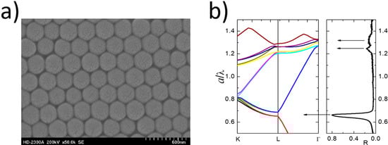
 The spatial period of structure “a” is called the lattice constant, analogous to the lattice constant in ordinary crystals, built of regularly arranged atoms [21][29]. The interaction of light with such periodic structures depends on their geometry, i.e., both on the type of crystal lattice, the shape of elements located in the nodes of the lattice [22][30], and the volumetric share of the material with a given refractive index in the unit cell, quantified by the value called the filling factor, f [23][31]. Another crucial parameter affecting such periodic structures’ properties is the contrast of individual areas’ refractive indices. The most crucial feature of photonic crystals is the photonic band gap (PBG) in the photonic band structure. Its presence can be verified by examining the spectral characteristics of the reflection or transmission (Figure 2).
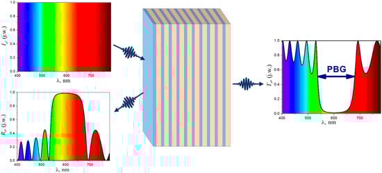 1D PCs are otherwise called distributed Bragg reflectors (DBR) (Figure 2). Generally, they are designed as narrow-band reflectors.
Two types of 2D PCs can be distinguished [25][26][34,35]: photonic crystals of the “hole” type, consisting of cylinders with a low refractive index embedded in a medium with a high refractive index [27][28][29][30][36,37,38,39], and the “rod” type, consisting of rods with a high refractive index surrounded by a medium with a low refractive index [26][31][32][33][34][35][36][35,40,41,42,43,44,45]. Both holes and rods can be arranged differently to create different 2D crystal lattices. The main factors determining the properties of two-dimensional photonic crystals are the refractive index contrast, the degree of filling with a material with a high or low refractive index, and the type of crystal lattice. In 2D structures, the formation of a two-dimensional PBG requires the fulfillment of additional conditions [37][38][46,47], such as the appropriate geometry of the structure and a sufficiently high contrast of refractive indices [38][39][40][47,48,49]. The greater the contrast, the wider the total PBG is. Depending on the structure, the PBG may exist only for the TM or the TE mode [25][41][42][33,34,50]. Only in exceptional cases is a two-dimensional photonic band gap obtained for both polarizations [43][44][51,52], like in the “honeycomb” lattice.
Generally, better results were achieved in the case of ternary 1D PCs (e.g., [64][71]). To enhance the absorption, the authors of [64][71] combined multilayer ARC with inverted pyramid texturing on the top layer.
Two-dimensional photonic crystals (see, for example, Figure 4e,f) can also be utilized for antireflection [71][72][73][77,78,79] and light trapping [48][74][75][76][77][80,81,82,83,84] covers (see Table 4). Two main types of optical effects are commonly used in such structures: one based on geometric optics and the other based on wave optics [78][85]. The first relates to the shape conducive to multireflection and consequently improves absorption. The second approach is based on the peculiar properties of photonic crystals.
In 2010, Hung et al. [71][77] applied 2D PCs with tapered rods to achieve antireflection and enhanced absorption. That structure reduces the reflection due to a gradually changed effective index. On the other hand, strong optical resonances for TM-mode can be found in this structure, mainly due to the complete photonic band gap inside the material. Such resonance can enhance the optical absorption inside the silicon PCs due to its increased optical paths [71][77]. In 2013, surfaces with micropyramids (Figure 4c) were used in commercial solar cells as part of an antireflection strategy [72][78]. Dominguez et al. [72][78] optimized 2D photonic crystals (PCs) onto Si wafers to improve the performance of c-Si solar cells. Their objective was to find a structure capable of minimizing the reflectance of the Si wafer in the spectral range between 400 nm and 1000 nm. They analyzed both hole-type and rod-type 2D PCs (see Figure 4e,f) with different shapes of holes (inverted pyramids, square holes, round holes) and rods (round pillars, cones, square pillars) and different crystal lattices (square, hexagonal, rectangular) [72][78]. The pattern of circular pillars arranged in a square lattice with a pitch of 448 nm, a diameter of 325 nm, and a height of 138 nm (a) was found to be the best structure, with an average reflectance of 3.6% in the spectral region from 400 nm to 1000 nm. This value was obtained without any other material used as an anti-reflective coating.
Shen Hong-Jun et al. [79][86] designed a solar cell with an antireflection layer in the form of regularly arranged dielectric cylinders with a truncated cone shape. They used Si3N4 to form cones and SiO2 as a substrate. [78][85]. Kuang et al. [75][80][81,87] proposed a unique teepee-like PC on crystalline silicon (c-Si). This structure is characterized by excellent antireflection due to its Gaussian-type gradient index profile. It also enhances light trapping due to its near-orthogonal energy flow and vortex-like field concentration via the parallel-to-interface refraction effect inside the structure. On the other hand, the structure optimized for light-trapping, e.g., a teepee-like structure, may act as a surface recombination center and reduce solar cell efficiency [77][84]. Bhattacharya and John state that the most likely candidate for high-efficiency silicon solar cells consists of inverted micropyramid PCs [81][21].
It is worth mentioning that some authors treat inverted pyramid structures as a type of texture [64][82][71,88], while others treat them as PCs [83][84][85][89,90,91], calling them surface PCs [85][91]. If the lattice spacing is comparable to the desired wavelength, light trapping should be enhanced by robust wave interference in the photonic structure [83][89] and resonant effects [85][91]. However, according to Razzaq et al. [86][92], the influence on the efficiency of random pyramid texturing is comparable with a periodic inverted nanopyramid structure. A further study [87][93] showed that an optimized inverse nanopyramid regular structure could outperform the random pyramid texture when considering incidence angle variations.
These structures, playing the role of ARC, simultaneously contribute to light trapping, absorption enhancement, radiation cooling, etc.
Selected solutions are presented in subsequent chapters. Very often, the choice of structure is dictated by the technological capabilities required for PC production. However, one can also come across proposals for more sophisticated structures, such as photonic crystals comprising gyroidal and hyperbolic layers [59][66]. The advantage of such a structure is an angle-insensitive reflector for solar energy applications, such as reflectors, a wavelength-selective absorber, smart windows, and an intermediate layer for solar cells.
 In the 1980s, Green et al. had already conducted a computer-based analysis of a double-layer antireflection phenomenon [61][68]. They found that a combination of a quarter wavelength of ZnS (refractive index, n = 2.25–2.35) and a quarter wavelength of MgF2 (n = 1.35–1.40) provided the best results (both thicknesses referred to a vacuum wavelength of 600 nm) in the case of silicon solar cells. It is possible to keep reflection loss below 2% from 460 to 940 nm with such a coating [61][68]. Multilayer antireflection structures (Figure 4d) have also been analyzed [65][66][72,73]. Womack et al. found that stacks of two SiO2 and two ZnO2 alternating layers of various thicknesses on thin film CdTe solar cells reduced their average reflection to ~1.2% [65][72]. Multilayer systems can be referred to as 1D PCs, provided that the periodicity of the layer system is maintained. These structures, commonly called distributed Bragg reflectors, are typically engineered to serve as narrow-band reflectors. However, their transmittance is almost negligible in the photonic band gap range wavelength. Regardless, applying 1D PCs as an ARC has been considered [62][64][67][68][69][70][26,69,71,74,75,76]. The consideration is often limited to the one-period photonic crystal structures [64][67][68][70][26,71,74,76], meaning multilayer structures are analyzed. The details of the examined 1D structure are presented in Table 3. Most of the works concern only theoretical considerations. An attempt to obtain the analyzed structure was made by Bennet’s group [69][75]. They used reactive sputtering to fabricate non-stoichiometric silicon oxynitride (SixOyNz) layers whose refractive index ranges typically from 1.4 to 1.7, depending on content.
 1D multilayer structures [62][107][69,113], 1D photonic ribbon structures [108][114], and 3D inverse opals [106][107][109][25,113,115] as IRLs have been considered theoretically and experimentally. O’Brien et al. [107][113] compared solar cells’ properties with different IRLs, like 1.5-bilayer and 3.5-bilayer μc-Si/ZnO (acting as Bragg reflectors) and ZnO inverse opal. One of their conclusions was that the Bragg reflectors provide a larger band gap and less parasitic absorption than the analyzed inverted opal PC. The constituent materials of 1D binary PCs designed for c-Si/a-Si tandem solar by Sayed et al. [62][69] were Bi4Ge3O12 and μc-SiOx:H. They examined ten-period structures consisting of a 62 nm layer of Bi4Ge3O12 and μc-SiOx:H layers with different thicknesses (40 nm, 55 nm, and 73 nm) depending on the sample. However, they observed the widest PBG (400–730 nm) when stacked with all three structures.
Sundar et al. [105][112] theoretically designed a 1D magnetic photonic crystal (MPC) as a multilayer system of a metal-doped magnetic composite material (Cu-YIG) and μc-SiOx:H. They found that the photonic bandgap of MPC increases with the number of periods and the percentage of copper doping, which tends to enhance the light trapping in tandem solar cells.
A completely different 1D structure was demonstrated by Amiri et al. [108][114]. It was a one-dimensional silicon strip with a 200 nm breadth and a length of 18 μm with ten air holes etched on it. The air hole diameter was 180 nm and the lattice spacing was 1.75 μm. The structure parameters were matched to reflect the light of wavelengths from the specific range thanks to a photonic band gap. The reflected signal was absorbed by the upper cell, and the transmitted signal was absorbed by the bottom cell.
The other type of investigated IRL is inverse opal [106][107][109][25,113,115]. In 2008, Bielawny et al. [106][25] prepared a thin film of ZnO inverse opal at the rear side of a-Si solar cells with the intention of later integration with c-Si/a-Si tandem solar cells. Upping et al. [109][115] examined the impact of the IRL in the form of ZnO:Al inverse opal on the c-Si/a-Si tandem solar cell external quantum efficiency. They reported an increase in the enhancement of the external quantum efficiency in the a-Si:H layer with a factor of 3.6.
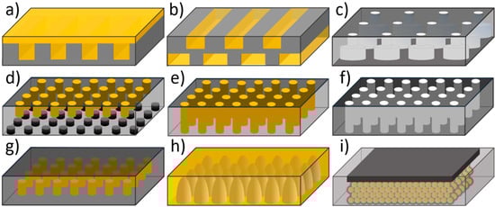

Figure 1. Models of photonic crystals: (a) one-dimensional (1D), (b) two-dimensional (2D), (c) three-dimensional (3D). The different colors represent materials with various refractive indices.

A large variety of 3D PCs exist. Some of the most popular are Yablonovite, consisting of a triangular system of holes prepared by drilling the slab at a specific angle, woodpile, formed “layer by layer” by a stock of dielectric 1D bars with alternating orthogonal orientations, opal or inverse opal, obtained by self-organization from monodisperse colloidal suspensions. Similar to 2D structures, the properties of 3D PCs depend on the geometry, degree of filling, and contrast in refractive indices [41][33]. An exemplary 3D photonic crystal in the form of SiO2 opal and its corresponding photonic band structure compared with reflection spectra are presented in Figure 3 [45][53].

3. Photonic Crystals in Photovoltaics
Photonic crystals can be applied in solar cells to enhance their performance and efficiency through better light management and trapping. They can be used as:-
Anti-reflective and light-trapping surfaces
-
Back reflectors
- Spectrum splitters
| MgF | ||
| 2 | ||
| /ZnS/Al | ||
| 2 | ||
| O | ||
| 3 | ||
| 92.39 nm/109.91 nm/ | 78.70 nm |
- Absorption enhancers
Table 4.
Details of 2D PCs used as anti-reflective and light-trapping surfaces.
- Additional light management layers
- Radiation coolers (RCs)
-
Electron transport layers (ETLs)
Table 2. The values of power conversion efficiency (PCE) and its increase (ΔPCE) as a result of the use of PCs. For comparison, the values of ΔPCE were calculated according to the formula (PCEPC−PCEr)/PCEr where PCEPC is the efficiency of SCs with PCs and PCEr is the efficiency of reference SCs without PCs. *: value is taken from the reference literature.
| Square | ||||
| Hexagonal | Rectangular Square Square Hexagonal Square |
On <100> silicon | Theoretical and experimental | |
| [76][82] | Holes in ITO/p-AlGaAs layer | Hexagonal | GaAs | Theoretical |
| [73][79] | Nanocylinders of Al2O3 or PMMA | Square a = 440 nm |
GaAs Si |
Theoretical |
| [74][80] | Inverted nanopyramid surface texture | Thin-film c-Si | Theoretical and experimental | |
| [75][81] | Teepee-like PC | a = 1200 nm | c-Si | |
| [48][83] | Parabolic-pore thin-c-Si inverted pyramid |
a = 1000 nm | Thin-film c-Si | Theoretical |
| [77][84] | Inverted micropyramid surface texture | a = 1300 nm, 1800 nm, 2100 nm, and 2500 nm, |
Thin-film c-Si | Theoretical |
3.2. Back Reflector
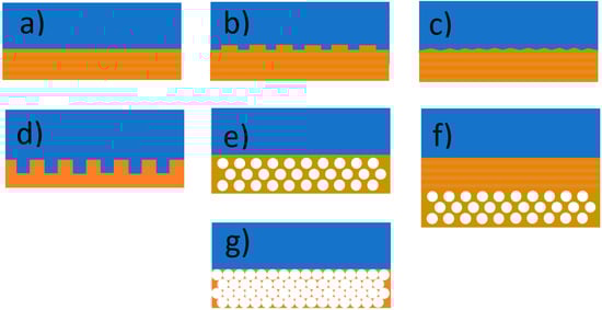
It is vital to prevent light from escaping from the active layer without being absorbed. This condition requires a relatively thick active layer (even up to 3 mm) in most popular silicon solar cells [88][94]). Back reflectors are applied to reduce this thickness. They reflect the light passing through the active layer back to the active region and enhance the path along which light can be absorbed. The simplest back reflectors are metal layers [76][89][82,95], for example, Ag [75][88][81,94] or Al [88][90][94,96]. However, they have some drawbacks (plasmonic resonance loss of the interface between the metal and absorption layers, performance degeneration due to metal ion diffusion) [88][94]. PCs find their application in thin film solar cells by providing controllable and enhanced reflections from material layers to promote increased absorption. The wavelength range and intensity of reflection depend on the PBG and can be easily adjusted thanks to a geometrical dimension of the PC structure. It allows for the easy optimization of 1D PCs concerning specific requirements. There have been a large number of propositions for using PCs as a back reflectors (Figure 5):
Figure 5. Different photonic crystal back reflectors: (a) 1D (DBR); (b) 1D with a reflection grating; (c) textured 1D; (d,e) 2D; (f) the combination of 1D and 2D; (g) 3D inverse opal.
| Reference | Solar Cell | Type of PC | Function of PC | PCE, % | ΔPCE, % | Methodology |
|---|---|---|---|---|---|---|
| [47][187] | Perovskite | 2D honeycomb-like | Light management | 20.85 | 12.1 | Experimental |
| [48][83] | c-Si | 2D parabolic-pore inverted pyramid | Light trapping | 29.11 | 6.8 | Theoretical |
| [49][111] | c-Si | 3D inverse opal | Back reflectors | 30.43 | 16.0 | Theoretical |
| [50][109] | Thin film CdTe | 2D lattice of rods | Back reflector | 25.51 | 23.1 | Theoretical |
| [51][103] | CdS/CdTe-based | 1D multilayer | Back reflector | 10.47 | 26.7 | Experimental |
| [52][179] | Polymer | 1D multilayer | Back reflector | 8.20 5.41 |
23.3 26.4 |
Experimental |
| [53][188] | Perovskite | 2D lattice of rods | Absorption enhancer | 20.97 | 20.9 | Theoretical |
| [54][189] | Dye-sensitized | 3D inverse opal | Absorption enhancer | 6.875 | 21.7 | Experimental |
| [55][190] | Organic | 1D multilayer | RC | 8.98 | 1.5 | Theoretical |
| [55][190] | Perovskite | 1D multilayer | RC | 12.5 | 2.4 | Theoretical |
| [56][173] | Thin-film c-Si | 1D multilayer with the SiO2 grating | RC | - | 0.45 * | Theoretical |
| [57][183] | Hybrid perovskite | 3D inverse opal | ETL | 13.11 | 19.2 | Theoretical |
| [58][184] | Perovskite | 2D lattice of hemispheres | ETL | 15.2 | 44.7 | Experimental |
| [12] | Perovskite | 2D array of nanodisks | ETL | 18.70 | 19.6 | Experimental |
3.1. Anti-Reflective and Light-Trapping Surface
When electromagnetic radiation falls on the interface of two transparent media, generally, two phenomena occur: Part of the radiation passes from one medium to another, undergoing refraction, and the rest reflects from the interface. The more radiation is reflected, the less radiation passes inside. The bare silicon, still the most common material used in solar cells, in intimate contact with air, reflects approximately 35% of the incident power over all wavelengths used in solar cell work [60][67]. Thus, applying anti-reflective coating (ARC) or surface texturization is crucial to improve the efficiency of a solar cell [61][62][68,69]. They aid in preventing reflection and ensure as much radiation as possible penetrates the active layer, particularly of the wavelength range that interacts with the given material. Different antireflection coatings have been optimized theoretically and experimentally so far (Figure 4). The simplest ARC consists of a thin layer of dielectric material (Figure 4a) with a specially chosen thickness so that interference effects in the coating cause the wave reflected from the ARC top surface to be out of phase with the wave reflected from the semiconductor surfaces [63][70]. The layer type and thickness depend on the material used in a solar cell. The dielectric contrast between the air and material of the solar cell should be reduced to reduce the reflection spectrum [64][71]. For instance, Fedawy et al. [63][70] examined the efficiency of GaAs solar cells covered with a Si3N4 antireflection layer. They increased efficiency from 14.89% to 27.16% by adding 75 nm Si3N4 ARC and 29.57% after additional front surface texturing (Figure 4b).
Figure 4. Different anti-reflective and light trapping surfaces: (a) interference thin film; (b) texturized thin film; (c) texturization in the form of a regular set of, e.g., micropyramids; (d) 1D photonic crystal; (e) rod-type 2D photonic crystal (f) hole-type 2D photonic crystal.
Table 3.
Details of 1D PCs theoretically analyzed as ARC.
| Reference | Type | No. of Periods | Materials | Optimum Thickness | Solar Cell |
|---|---|---|---|---|---|
| [67][26] | Ternary | 1 | SiO2/Si3N3/SiO2 | 98 nm/48 nm/8 nm | PIN silicon |
| [68][74] | Ternary | 1 | SiO2/KBr/SiO2 | 98 nm/48 nm/8 nm | PIN silicon |
| [69][75] | Binary | 1 or 2 | SixOyNz | a-Si:H | |
| [64][71] | Binary | 1 | SiO2/TiO2 | 54 nm/82 nm | a-Si |
| [64][71] | Ternary | 1 | SiO2/Si3N3/TiO2 | 54 nm/33 nm/82 nm | a-Si |
| [62][69] | Ternary | 1 | SiO |
- Textured conductive PCs (TCPC)
- [
3.3. Spectrum Splitter
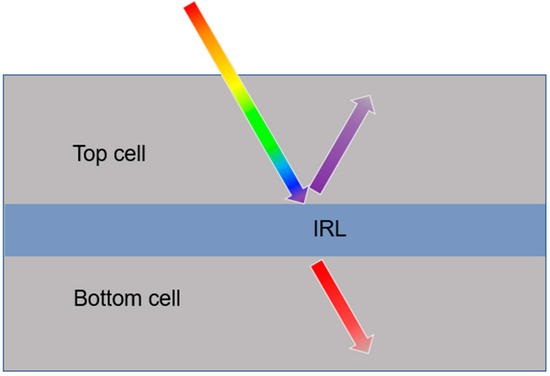
Tandem solar cells are created for conversion power over a wide energy spectrum. Such cells consist of two or more layers of material having different energy gaps. The layer with the higher energy gap is placed at the top, and the layer with the lower energy gap is placed at the bottom (Figure 6). The most commonly used combination of materials is c-Si and a-Si [105][112]. Such a structure requires an additional intermediate reflected layer (IRL) for spectrum splitting and light management between these layers. The non-absorbed photons with shorter wavelengths should be reflected to the top layer of the solar cell, and the photons with longer wavelengths should be transmitted to the bottom one [62][69]. Photonic crystals are perfect for designing an IRL (see Figure 2). Moreover, the IRL must possess adequate electrical conductivity to prevent any losses through ohmic resistance in the interconnection of the active layers [106][25].
Figure 6.
Schematic light propagation through a tandem solar cell structure with IRL.
3.4. Absorption Enhancer
The Lambertian limit serves as a crucial benchmark in assessing the efficiency of solar cells [110][116]. Research has indicated that both extremely thick and extremely thin solar cells can approach this limit by implementing effective photon management strategies. By optimizing techniques for managing photons, these cells can operate closer to the Lambertian limit, resulting in improved overall performance. One way to enhance absorption is to use an active layer of SC in the form of a PC. Ordered photonic crystals have highly localized diffraction profiles and offer strong coupling to optical modes at specific wavelengths, with corresponding absorption enhancements that can exceed the Lambertian limit [111][117]. A periodic structure leads to nonlinear dispersion, which results in flat photonic bands and the appearance of band gaps in photonic crystals. The group velocity of light with wavelengths close to band gaps is anomalously low, and the so-called slow photon effect is observed [112][118]. The lower light velocity increases the effective optical path of light [113][119]. Thus, when the edge of the PBG overlaps with the electron absorption edge, the result can be expected to enhance light absorption [113][119]. The absorption edge can be tuned by varying the dimensions of the periodic structure, thereby moving the PBG [114][120]. This effect occurs for the photonic band gap’s red and blue edge [115][121]. Many authors explain absorption enhancement by the existence of slow photons [11][115][116][117][118][11,121,122,123,124]. However, Mihi and Miguez [115][121], examining dye-sensitized SCs as a combination of a photonic crystal and a layer of nanocrystalline absorbing material, concluded that absorption enhancement due to resonant modes localized within the absorbing coating brings a better effect than slow photons in the active layer of the PC form. Therefore, photonic crystals play only the role of porous colloidal mirrors operating through coherent scattering [115][119][121,125]. Coupling to the resonant modes was also considered by other authors [85][110][120][121][91,116,126,127], even in the case of the PC active layer [121][127]. Another explanation based on tuning the coupling strength of incident radiation to quasi-guided modes over a broad spectral range using the PC structure appears in refs. [122][123][124][125][128,129,130,131]. Such coupling enables the photons to spend enough time in the patterned active layer to be absorbed there [121][127]. The other mechanism for absorption enhancement in photonic crystals arises from strong resonances from parallel interface refraction (PIR) [126][132]. This anomalous refraction type is negative and usually out of the plane of incidence. Light impinging on photonic crystals over a wide range of frequencies couples to Bloch modes and propagates nearly parallel to the thin film-to-air interface. This phenomenon leads to anomalously long optical path lengths and a long time before the light beam exits the thin film. This effect can be much stronger than that of slow photons. Various photonic crystal structures, for example, 1D grating [11][123][127][11,129,133], 2D structures [7][110][117][118][121][122][124][125][128][129][7,116,123,124,127,128,130,131,134,135], and 3D structures [115][116][119][130][121,122,125,136] have been investigated for solar cell applications (see Figure 7).
Figure 7. Examples of PC structures in the active layer: (a) 1D grating based on [123][129]; (b) double 1D grating based on [11]; (c) double layer of 2D PCs based on [122][128]; (d) double 2D PCs based on [110][116]; (e) 2D lattice of cylinders based on [117][123]; (f) 2D lattice of air cylinders based on [7][121][7,127]; (g) 2D PCs based on [118][124]; (h) lattice of nanocones based on [125][131]; (i) inverse opal based on [119][125].
