Submitted Successfully!
To reward your contribution, here is a gift for you: A free trial for our video production service.
Thank you for your contribution! You can also upload a video entry or images related to this topic.
Version Summary Created by Modification Content Size Created at Operation
1 -- 4606 2023-08-22 09:13:13 |
2 format change Meta information modification 4606 2023-08-22 10:51:48 |

Video Upload Options

Do you have a full video?

Confirm

Are you sure to Delete?
Cite
If you have any further questions, please contact Encyclopedia Editorial Office.
Vorobyova, M.; Biffoli, F.; Giurlani, W.; Martinuzzi, S.M.; Linser, M.; Caneschi, A.; Innocenti, M. Physical Vapor Deposition for Decorative Applications. Encyclopedia. Available online: https://encyclopedia.pub/entry/48303 (accessed on 23 July 2024).
Vorobyova M, Biffoli F, Giurlani W, Martinuzzi SM, Linser M, Caneschi A, et al. Physical Vapor Deposition for Decorative Applications. Encyclopedia. Available at: https://encyclopedia.pub/entry/48303. Accessed July 23, 2024.
Vorobyova, Mariya, Fabio Biffoli, Walter Giurlani, Stefano Mauro Martinuzzi, Maximilian Linser, Andrea Caneschi, Massimo Innocenti. "Physical Vapor Deposition for Decorative Applications" Encyclopedia, https://encyclopedia.pub/entry/48303 (accessed July 23, 2024).
Vorobyova, M., Biffoli, F., Giurlani, W., Martinuzzi, S.M., Linser, M., Caneschi, A., & Innocenti, M. (2023, August 22). Physical Vapor Deposition for Decorative Applications. In Encyclopedia. https://encyclopedia.pub/entry/48303
Vorobyova, Mariya, et al. "Physical Vapor Deposition for Decorative Applications." Encyclopedia. Web. 22 August, 2023.
Physical Vapor Deposition for Decorative Applications
Edit

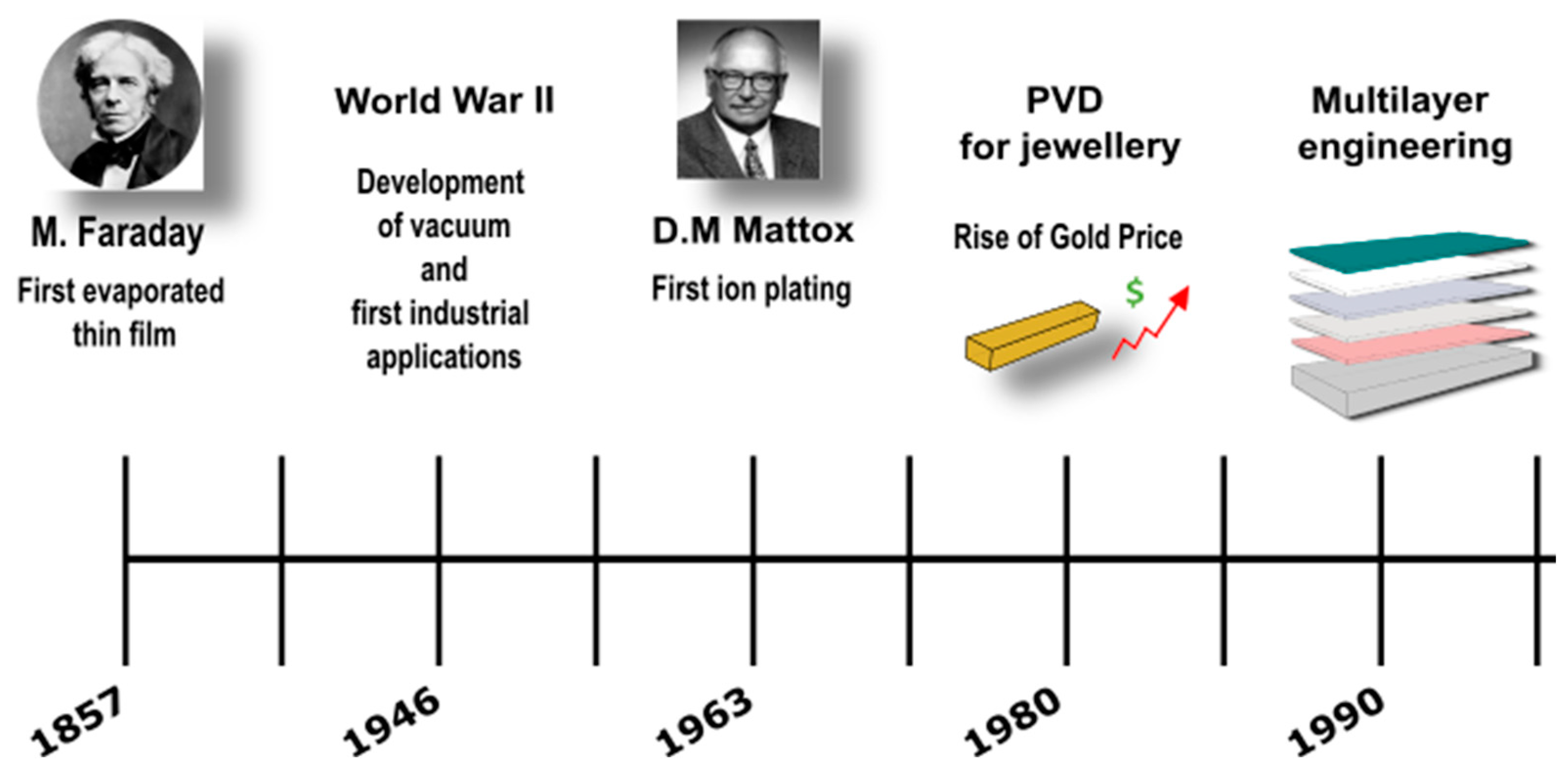
Physical Vapor Deposition (PVD) is a widely utilized process in various industrial applications, serving as a protective and hard coating. However, its presence in fields like fashion has only recently emerged, as electroplating processes had previously dominated this reality. The future looks toward the replacement of the most hazardous and toxic electrochemical processes, especially those involving Cr(VI) and cyanide galvanic baths, which have been restricted by the European Union. Unfortunately, a complete substitution with PVD coatings is not feasible. The combination of both techniques is employed to achieve new aesthetic features, including a broader color range and diverse textures, rendering de facto PVD of primary interest for the decorative field and the fashion industry.

PVD coatings fashion decorative thin-film characterization sputtering magnetron physical vapor deposition

1. Introduction

The physical vapor deposition (PVD) process has been applied since the early 1900s, but most of its development occurred in the 1960s and 1970s, becoming extensively utilized in industrial applications (Figure 1). Advancements in vacuum technology and deposition techniques have expanded the range of substrates to which PVD thin films can be applied, allowing for greater control over the properties of these films. Today, PVD technology is still to be improved; new materials, new techniques, as well as cost reduction have enabled applications in sectors such as the aerospace [1], automotive [2], electronics [3] and even fashion industry [4]. Specifically, the fashion industry has recently embraced PVD to develop more sustainable manufacturing processes. This research aims to overview both the state-of-the-art of PVD and the research perspectives.
Figure 1. Historical timeline of thin-film evolution connected to the most relevant events, which highlights the significant innovations in PVD techniques.
The first evaporated thin films can be traced back to Faraday’s experiment in 1857 [5], where he evaporated metal wires in a vacuum. Subsequently, in 1887, Nahrwold [6] replicated the deposition of thin metal films in a vacuum, following Joule’s heating experiments. A year later, Kundt [7][8] measured the refractive indices of such films. The application of this technology on an industrial scale had to wait for the development of vacuum techniques, which emerged after World War II, around 1946. The exponential growth rate of thin films is well-documented in Olang’s excellent review of deposited films in the Handbook of Thin Film Technology, as well as Holland’s classic textbook [8] reflecting the substantial pioneering work performed by the author.
The ion plating technique was first described by Mattox [9] in 1963, although a similar technique had previously been reported by Berghaus, who claimed that the coating had “a perfect structure and adhering strength”, even for thicker layers. It was Mattox that stimulated considerable interest and spurred the development of these techniques. Mattox asserted that the technique produced films with exceptional adhesion, even when the film and substrate materials were mutually insoluble. Moreover, the films exhibited thick uniformity and effectively coated irregular surfaces. Many subsequent investigations have since confirmed these findings.
The first metal deposits realized through glow discharge plasma were reported by Grove in 1852 [8]. In 1980, sputtering and its applications experienced rapid growth, with advancement in the apparatus, process modifications, scientific understanding, and expanded application areas, similar to other PVD techniques.
In 1961, two independent US universities initiated research on high deposition rates and full-dense PVD coatings on self-supported shapes. At the Lawrence Livermore Laboratory of the University of California, Bunshah and Juntz [10] produced high-purity beryllium foil and titanium sheet and characterized them in terms of impurity content, microstructure, and mechanical properties. During the same years, Smith and Hunt at Temescal Metallurgical Corporation in Berkeley, California focused on the depositing of various metals, alloys, and compounds.
In the early 1960s, USSR scientists began their work on thin- and thick-film deposition at the Kharkiv Polytechnique Institute, and later at the Paton Electric Welding Institute in Kiyv. Between 1962 and 1969, various steel companies dedicated significant efforts to producing Al and Zn coatings on steel using PVD processes on a production scale [11].
In 1969, Airco Temescal Corporation [12] successfully manufactured Ti-6AZ-4V alloy foil. Pilot production quantities were adopted in honeycomb structures on the SST aircraft, although the aircraft project ultimately failed. The production capability was impressive, with a production rate of 1200 ft per run of Ti-6AQ-4V foil, 12″ wide and 0.002″ thick at a rate of 2–3 ft per minute; moreover, the cost was significantly lower than rolled material.
Studies of thin films had advanced before thick- and bulk-film technology, as documented by Bunshah [13] and Paton, Movchan, and Demchishin [14]. Soviet literature also includes numerous references to the great work on thin and thick films by Palatnik of the Kharkiv Polytechnique Institute. The development of ion plating and sputtering processes continued progressing rapidly and interactively, repeating substantial benefits from their shared characteristics [15].

2. Fundamentals of Physical Vapor Deposition (PVD)

Physical Vapor Deposition is a widely used technique for depositing thin films, both in basic and applied research, as well as in various industrial sectors. It finds extensive uses in realizing protective coatings for biomedical applications and in developing thermal barrier systems (especially for aircraft engines) [16][17], in optics [18], and in electronic components manufacturing [19]. These coatings can improve the substrate’s performance by increasing hardness, wear [20], and corrosion resistance; improvements in tribological [21], optical, and electrical properties are also reported. A combination of these properties is often required [22].
PVD is a vacuum-based technique that involves depositing a thin layer or multilayers of target materials onto a substrate. The thickness of coatings ranges from a few angstroms to several microns, and the deposition rate depends on various operating parameters, including the total pressure in the chamber [23], the partial pressures of the carrier and the reactive gases [24], power and source of usage [25], voltage biases [26], temperature [27], and the sputtering yield of the target [28]. It is important to note that in industrial practice depositing hard coatings is just one step in a sequence of operations that includes the mechanical preparation of surfaces, cleaning, heating, etching, coating, cooling, and conditioning; the weakest link in this chain, therefore, defines the overall quality of the coating. In some cases, specific steps may be skipped; however, this does not make things easier because methods and operating parameters for the remaining steps vary significantly depending on the coating material, the process used, and the desired final performance specifications [29].
During the deposition process, the material is vaporized from a solid into an atomic or molecular form and transported through a vacuum or low-pressure gas environment or plasma (Figure 2) towards the substrate, where it condenses. Vacuum deposition typically takes place in a chamber with a pressure range of 10−5 Torr to 10−9 Torr, depending on the level of gas contamination that can be tolerated. The rate at which deposition occurs ranges from 10 Å/s to 100 Å/s and it can be influenced by many factors, such as evaporation or the sputtering yields of materials. For instance, gold has a higher deposition rate than chromium under the same conditions.
Figure 2. Example of plasma production in magnetron sputtering system.
Additionally, the deposition rate is lowered by improving the gas pressure via the addition of both carrier gas (Ar is the most used for this purpose) and reactive gas (O2, N2, acetylene), increasing their flow rate (expressed in Sccm, Standard cubic centimeters per minute), or through target poisoning, which can create a hysteresis effect [30][31]. A proper adjustment in the voltage bias and (sample heating) temperature can produce better film properties, such as high density and improved adhesion [32][33].
Over the years, the advancement of technologies in the construction of automated production plants has allowed the scale-up of various PVD deposition techniques [34].

3. Substrates

PVD coatings can be deposited on several substrates, such as, Ti, Al, Cu alloys, steel, and even plastics (e.g., polycarbonate [35]). Corrosion-resistant substrates are preferred because PVD coatings’ corrosion performances are highly dependent on the microstructure. The well-known columnar structure, typical of PVD films, is due to the line-of-sight process, often associated with a not negligible degree of porosity. Voids within the coating could be the starting points for substrate degradation processes [36]. This is just one of many aspects to keep in mind when choosing substrate material for industrial applications. The compatibility with PVD processes is an often-overlooked aspect in base material selection. The main drivers are the raw material cost, the ease of working, and the suitability for large-scale manufacturing. The benefits and drawbacks of using brass and steel as substrates in industrial deposition processes are summarized in Figure 3.
Figure 3. Schematic description of main advantages and disadvantages of brass and steel as substrates.

4. Surface Finishing

4.1. Titanium-Based Coatings

Decorative titanium-based coatings have been widely used in the industry due to their biocompatibility [37], color options [38], remarkable corrosion resistance [39], and cost-effectiveness. TiN coatings can be prepared by adjusting the vacuum to 5 × 10⁻⁵ Torr, heating the substrate to 100 °C, and using 4 A of input current. In these conditions, nitrides like TiN [40] and ZrN [38] can be deposited; these have been extensively researched for a variety of industrial applications such as hard coatings [39], diffusion barriers in semiconductor technology, mirrors for optical applications [41][42], and decorative coatings.
Several factors influence the deposition of TiN coatings, such as the reactive gas used, the total pressure in the chamber [43], Ar/N2 ratio [44], substrate temperature [45], and the substrate’s bias voltage [46][47]. Among these factors, nitrogen flow is the most crucial because it determines the color of the coatings. The deposition conditions that produce the brightest yellow must be chosen precisely. For instance, a mistaken N2 supply can produce unaesthetic dull colors [48]. The watchmaker industry developed the historical process for gold coating, which involved covering a thin layer of titanium nitride with a flash of gold to create a highly wear-resistant coating. Combining TiN and ZrN layers, a gold-like appearance has been successfully obtained in producing luxury pens [49].
Carbides are prepared similarly to nitrides, using acetylene instead of nitrogen as a reactive gas; they are an alternative to the most expensive DLC for the realization of black coatings, albeit with lower hardness and stress resistance. To overcome these drawbacks, Gupta in 2019 [50] proposed a new type of black coating, i.e., TiAlCO, using ion implantation. The Ti surface was bombarded with energetic carbon ions, applying 2 kV anode voltage and a 0.03 T magnetic field. A carbon-rich plasma was established at 2 × 10⁻⁶ h·Pa and a minimum ion fluence of 1018 C·cm−2 was necessary to achieve a black color surface.
Blue-colored coatings based on TiNO or ZrNO can be obtained by increasing the oxygen content in the nitride lattice. Another well-known material for decorative applications is TiO2, thanks to the wide range of colors obtainable by varying the coating thickness [51].

4.2. Chromium-Based Coatings

Chromium is a popular choice for PVD coatings due to its excellent mechanical, thermal, and chemical properties [52]. Chromium coatings are widely used in a variety of industries, including the aerospace [53], automotive [2], and medical industries, due to their ability to provide high wear resistance, hardness [54], and corrosion resistance [55].
Chromium PVD coatings are known for their exceptional resistance to wear and abrasion, making them ideal for use in applications that involve high levels of friction or impact. Additionally, chromium coatings have a low coefficient of friction, which makes them ideal for use in applications where sliding or rolling contacts are involved [56], such as bracelets and anklets.
Another advantage of chromium PVD coatings is their ability to provide excellent corrosion resistance. Chromium is easily passivated, which means that chromium coatings can protect the underlying material from rust and other forms of corrosion. It is also worth noting that chromium PVD coatings can come in a range of different colors, from a bright silver color to a darker gunmetal gray. The color of the coating can be controlled by adjusting the deposition conditions, such as the gas mixture, pressure, and temperature. Chromium PVD coatings are of interest to the decorative industry as an alternative to ECD chromium. Shiny and highly reflective ECD chromium coatings are widely used and appreciated; those are generally obtained via electrodeposition from Cr(VI) baths. Hexavalent chromium is a known human carcinogen, and its use has been heavily restricted by the European Union [57]. PVD chromium competes with Cr(III) baths to fill the space left in the market by Cr(VI) baths, as trivalent chromium baths have considerable criticalities such as the high temperature and high voltage required and worse mechanical and aesthetic properties due to the presence of carbides formed during the electrodeposition. In 2022, Martinuzzi [58] published a comparative study between PVD chromium and ECD chromium, proving how PVD chromium coatings are a valid alternative to ECD deposits obtained from Cr(VI) solutions. He deposited Cr PVD on a copper substrate at 6.3 × 10⁻³ Pa pressure, heating the substrate at 300 °C, while the plasma current was set at 150 mA.

4.3. Zirconium-Based Coatings

Zirconium-based ceramic compounds are used as a top layer due to their peculiar mechanical and aesthetic capabilities; an exhaustive review of Zr(N, C, CN) properties was made in 2020 by Ul-Hamid [59]. The most famous Zr-based ceramic for decorative applications is ZrN thanks to its golden-like color. Already in the late 1980s, ZrN-based coatings were first investigated as a hard coating for industrial applications such as wear-resistant protective layers [60]. ZrN PVD coatings exhibit a wide range of color depending on the deposition parameters, ranging from yellow to silver and brown to gray. In the late 1990s, it was clear that, unlike TiN, the color was dominated by the microstructure and not by the stoichiometric composition [61] and it could achieve a higher brightness (L* > 90) [62]. Nitrogen partial pressure is fundamental for color control, and the gold-like color was obtained with a N2 flux of 8–10 sccm. In 2001, Nose [38] proposed a comprehensive explanation of how the color is influenced by deposition parameters. Then, in 2020, Ul-Hamid [63] made a complete review of deposition conditions that influence the mechanical properties of various Zr ceramic compounds. From a decorative perspective, it is interesting to note that the golden color of ZrN is more greenish than the one obtained with TiN, but the higher brightness makes ZrN more suited for Au + ZrN systems. It has been proved that with the wear of the top-deposited gold layer, a close matching in L* guarantees a more pleasant aesthetic effect than a satisfying matching in hue [64]. Klumdoung [65] obtained silver, brown, green-yellow, and blue ZrN deposits working at a high Ar flow rate (6 sccm) and varying the nitrogen flow from 0 sccm to 6 sccm, again reporting the correlation between color and crystal structure. The corrosion resistance properties of ZrN deposits are strictly correlated to structural parameters such the grain size [62], and according to Kuznetsova [66], deposit structure can be accurately tuned by optimizing the N2 flow. For decorative applications, multilayer Zn/ZrN systems are preferable due to their superior corrosion-resistance properties [67][68]. Multilayer ZrN/TiN systems can produce coatings with high hardness and stronger adhesion [69] compared with ZrN and TiN systems. Recent works have focused on improving ZrN’s mechanical and optical properties with the addition of Si and O as ternary elements [70][71][72]. Furthermore, to obtain coatings with antimicrobial capabilities [73][74], the addition of Cu to Zr-based ceramics has been evaluated. Gray PVD coatings can be achieved by depositing ZrC [75], but this top layer is uncommon in the decorative field since Cr-based coatings are preferred.

4.4. DLC Coatings

DLC coatings are amorphous carbon-based materials containing a mix of sp2 and sp3 hybridized C atoms. Their unique properties, such as high hardness, low friction, high thermal conductivity, and chemical inertness, rank among the two allotropic forms of carbon (graphite and diamond) and they depend on the sp2:sp3 ratio [76]. Raman spectroscopy is fundamental to characterize DLC: from D and G bands; it is possible to estimate the sp2:sp3 ratio and the internal stress [77][78]. DLC can be deposited by PVD using a graphite source and by CVD using a mixture of hydrocarbons as reactive gas [79]. The electrodeposition of DLC on Ti was achieved in 2009 by Manhabosco [80], but required a rapid increase in applied potential from 0 to 1200 V for 4 h and acetonitrile mixed with DMF as a medium; for their simplicity, PVD and CVD remain the best way for industrial applications. An in-depth analysis of DLC properties and classification was made in 2021 by Ohtake [81]. Due to their tribological and chemical properties, DLC coatings are widely used for cutting tools, engine parts, optics, and corrosion barriers, as reported by Vetter [82] in their historical review of DLC deposited by PVD for industrial applications from the first developments to 2014. DLC deposits are interesting for decorative applications because their black color, low friction, and wear resistance make DLCs great to be used as a finish on bracelets and watch bands [83]. DLCs are promising as a corrosion barrier too, but due to their high internal stress they are not suited to be an intermediate layer [75]. Low adhesion and delamination are the main problems that limit the usage of DLC in decorative applications. To improve the adhesion on a steel substrate, a Cr-based underlayer system was developed by Duminica in 2018 [21], and in 2021 Gómez [84] obtained a DLC coating on steel with surprising adhesion deposited with high-power impulse magnetron sputtering (HIPIMS) technology with positive pulses. For the DLC film, they used a graphite target operating at 600 V and 1.5 A.

5. Characterization of PVD Coatings

In decorative and high-end fashion industries, coating defects could compromise aesthetic properties, which are crucial in determining the commercial success of a product [85]. For this reason, accurate quality control planning of quality control is mandatory to reduce rejected products and increase company competitiveness [86]. A standard quality control protocol for PVD coatings has to include the evaluation of tribological properties (at least hardness and wear resistance), adhesion tests, corrosion resistance, and color measurements.

5.1. Thickness Determination

Probably the most common analysis in the decorative industry for PVD coatings is thickness determination [87]. Thickness is an important parameter, and it is correlated with other properties like adhesion, wear and corrosion resistance, and barrier properties [88][89]. The importance of layer thickness is amplified in modern multilayer systems, as their properties depend on the interface volume between layers [90][91]. As other important parameters for quality control, the thickness measurement methods of multilayer systems go under ISO 21874:2019 [92]. Thickness determination methods can be subdivided into destructive and non-destructive techniques. To examine multilayered structure methods involving Scanning Electron Microscopy (SEM) analysis, metallographic cross sections are preferable because they allow one to directly visualize and measure the multilayered structures. Other popular destructive techniques are the crater grinding method (regulated under ISO 26423:2016 [93][94]) and GDOES [95]. Thickness measurements methods based on X-ray fluorescence (XRF) and regulated under ISO 3497:2000 [94] are the most popular in industrial applications: they provide fast and accurate analysis, especially for metallic coatings, and various desktop ED-XRF, coupled with user-friendly software, are sold on the market for industrial applications. A new trend is the automatization of XRF measurements and the capability to obtain real-time data during the deposition [96] to improve further the quality control over the products. A standardless approach based on Monte Carlo simulations for XRF was proposed in 2019 [97]. Indirect thickness measurements with quartz microbalances (QCM) are also popular to perform real-time quality control on the deposited material over the surface [89]. To evaluate the thickness of thin films, Giurlani [98] developed in 2018 a standardless method based on EDS spectroscopy and Monte Carlo (MC) simulations: it was able to measure nanometric thicknesses of PVD-sputtered samples. In 2020, MC simulations were also employed with success to make calibration curves for XRF thickness measurements [99]. Another emerging non-destructive methodology was proposed in 2021 by Isern [100]; it is based on terahertz (THz) reflectivity and was successfully employed to map the PVD-deposited yttria-stabilized zirconia thermal barrier. In 2023, Cruz [101] proposed a standardless method, tested on TiN coatings, based on EDS and MC simulations that correlates the acceleration voltage, the type of substrate, and the intensity ratio of peaks of the substrate and the deposit to the coating thickness.

5.2. Mechanical Properties and Defects Analysis

Mechanical and tribological properties have been the subject of numerous studies [82][102][103][104][105][106][107]. In decorative PVD coatings, tribological properties play a critical role in determining the resistance of the coating to wear and abrasion, because they can affect the appearance and the lifespan of the coating. Therefore, coatings with good tribological properties such as high hardness, low coefficient of friction, and good wear resistance are preferred for decorative PVD applications. Several tribological parameters such as coefficient of friction, wear rate, and volume are evaluated with a pin-on-disk Tribometer; this test is regulated by ASTM G99-17 [108], DIN 50324-07 [109], and ISO 18535:2016 [110]. Hardness and adhesion are other important mechanical properties to evaluate the quality of a produced good: accessories and fashion jewels are subjected to continuous changes in temperature and frequent shocks and bumps. Small detachments or scratches that compromise the aesthetic value of the object determine the end of life of the product, as decorative goods lose functionality as soon as the visual appearance worsens and it is no longer desirable. Then, to improve the overall quality and reduce the embodied energy (the total energy required to produce a product, from raw material to the delivery of the final good), decorative PVD coatings need to pass hardness and adhesion tests. For hardness evaluation, indentation [111] tests are regulated by ISO 14577-1:2015 [112]. The Rockwell adhesion test is the one of choice to evaluate the adhesion of PVD coatings, as it provides quantitative information and it is regulated under ASTM C1624-22 [113] and VDI 3198 [114]; developments on automatizing and standardizing the Rockwell test involving neural networks and machine learning algorithms are ongoing [115]. Other adhesion tests are the network of cuts method under ISO 2819:2017 [116] and ISO 11644:2022 [117] and the tape test under ISO 11644:2022 [117]. A novel methodology, based on the crater grinding method and adhesion scratching tests, to obtain quantitative information on deformations and degradation of PVD multilayer films named the Recatest was proposed in 2021 by Domanowski [118]. Defect analysis is fundamental for PVD coatings due to the columnar structure and poor coverage of the deposits, and an excellent review of PVD growth defects was written by Panjan [36] in 2020. To differentiate defective products that could accelerate degradation processes and ensure the customer receives a high-quality product, the techniques to analyze PVD deposits, especially multilayer ones, are regulated under ISO 21874:2019 [92]; the election techniques are SEM analysis and Glow-Discharge Optical Emission Spectroscopy (GDOS) [119][120].

5.3. Color Evaluation

Color is probably the most important parameter for the haute couture and decorative industries: the main aim of a finishing coat in those fields is to provide aesthetic value to the artifact, increasing the perceived value, to make it a luxury and desired object. Several studies have been conducted on the importance of color and its implication in marketing and psychology [121][122], and the link between a good quality PVD coating and the precise color requested by a customer is so tight that it is mandatory to have a standardized and quantitative method to define, measure, and classify colors. Environmental factors (e.g., the source of illumination) and the intrinsic properties of objects can generate inconsistent data, causing disputes between manufacturers and customers. To avoid this, the color is usually encoded through the standard dictated by the L*a*b* color space (also known as CIELAB or CIE1976). The CIE (Commission International de l’Eclairage) establishes the procedures, lighting sources, and observation angles that can be used; those procedures are under ISO/CIE 11664:2019 [123]. The values of the three coordinates L*a*b* are obtained through the transforms relating to the X, Y, and Z coordinates of the color space CIE XYZ [124] and the mathematical treatment is already covered extensively in the literature [125]. The L*a*b* color space covers the entire gamut of the visible human spectrum and can be understood and represented as an opposite color model with b* that shifts from yellow (b* < 0) to blue (b* > 0), a* from green (a* < 0) to red (a* > 0). L* represents the brightness and goes from 0 (pure black) to 100 (pure white). Colorimetric measurements can be achieved with a cost-efficient tristimulus colorimeter [126], but modern colorimetric spectrophotometers are better suited to obtain accurate data and avoid disputes with the customer [127]. The accuracy required for the color of a PVD coating is usually determined by the customer in the form of a* ± Δa*, b* ± Δb*, and L* ± ΔL, but an important parameter to evaluate the quality of a product is the Euclidean distance (ΔE) inside the L*a*b* color space (1)
A just noticeable difference (JND) between two objects is detected by a human eye for ΔE ≥ 3 [128]. That threshold should be considered in the decorative PVD industry to evaluate the production quality.

5.4. Corrosion Tests

As mentioned in previous sections, the aesthetic properties of a PVD coating in the decorative industry are the main task to obtain and maintain. Visible corrosion-derived defects, even if they do not alter the mechanical properties of the goods, determine the end of life in the decorative field [64]. Produced goods, to meet customer acceptance, have to pass various tests that simulate and accelerate the environments where those objects are going to be used [129] (e.g., the atmospheric conditions of a bathroom, especially for faucet industries); especially for wearable products, they need to pass tests that simulate human beings (e.g., sweat). Corrosion tests and corrosion resistance properties are extensively indagated for PVD coatings [58][102][103][130][131]. In the decorative industry, a commonly used substrate is brass, and corrosion studies are needed to evaluate the performances that could be compromised by the columnar structure of PVD [120][132][133]. The most used regulated tests for quality control in the decorative industry are the salt spray test, divided into neutral, acetic acid, and copper variants (ISO 9227:2022 [134]); the synthetic sweat test (ISO 3160-2:2015 [135] and NF S 80-772:2010 [136]); electrochemical impedance spectroscopy tests (ISO/TR 16208:2014 [137] and ISO 16773 [138]); potentiostatic and potentiodynamic polarization measurements (ISO 17475:2005 [139]); tests that simulate pollution and corrosive atmospheres (thioacetamide test ISO 4538:1978 [140], sulfur dioxide and nitric acid tests regulated under ISO 4524:2000 [141]); and dump heat (with leather, ISO 17228:2015 [142], and without leather, ISO 4611:2010 [143]). For haute couture industries, damp heat with leather is important to simulate the contact with chrome-tanned leather: it has been proved that chrome-tanned leather releases oxidating agents in the form of Cr(III) and Cr(VI) [144][145] that could damage PVD-covered accessories.

5.5. Heavy Metals’ Release

Regarding wearable artifacts, the release of heavy metals is a fundamental parameter for ensuring the quality and safety of the product for the customer. Common hazardous metals in wearable PVD-coated artifacts are nickel and lead. Although lead and nickel thin films can be deposited by PVD [146][147], those coatings are not of interest for decorative applications, but both could be found in small quantities inside substrate alloys. Nickel-containing steel is the most used type of steel for PVD applications and lead is added to brass to increase its machinability [148], even if the trend is to employ new performing lead-free brasses [149]. In addition, as was mentioned before, electroplated nickel is widely used as a strike layer for PVD topcoats if brass is used as a substrate. Nickel is considered a hazardous element for human health and its issues concerning human health are well reported in the literature [150][151]; the most common problem related to nickel-containing wearable objects is nickel allergy [152]. Nickel-release tests have to be carried out according to EN 12472:2020 [153], which regulates methods that simulate the wear and corrosion of artifacts for the detection of nickel release; nickel determination is regulated under EN 1811:2015 [154] and an accurate report of the techniques used to quantify nickel release in decorative industries was accomplished by Giurlani [155]. Lead needs to be considered one of the most important toxic heavy metals in the environment, and its full spectrum toxicity is reported in a 2015 review by Wani [156]; in the European Union, lead percentage in alloys is regulated by the European Chemical Agency (ECHA) and only alloys with lead content of a weight lower than 0.05% are admitted in jewelry. Other important regulations are the US standard ASTM F2999-19 [157] for adult’s jewelry, which sets a 1.5% threshold for lead in alloys, and the US standard ASTM F2923-14 [158] for children’s jewelry, which sets the threshold at 0.01% [159]. Determination of lead content in a sample is regulated under CPSC-CH-E1001-08.3 [160], ISO 26482:2010 [161], and EPA 6010C:2014 [162].

References

  1. Jawaid, A.; Koksal, S.; Sharif, S. Cutting Performance and Wear Characteristics of PVD Coated and Uncoated Carbide Tools in Face Milling Inconel 718 Aerospace Alloy. J. Mater. Process. Technol. 2001, 116, 2–9.
  2. Baptista, A.; Pinto, G.; Silva, F.J.G.; Ferreira, A.A.; Pinto, A.G.; Sousa, V.F.C. Wear Characterization of Chromium PVD Coatings on Polymeric Substrate for Automotive Optical Components. Coatings 2021, 11, 555.
  3. Rossnagel, S.M. Sputter Deposition for Semiconductor Manufacturing. IBM J. Res. Dev. 1999, 43, 163–179.
  4. Bandinelli, R.; Fani, V.; Bindi, B. Electroplating and Pvd Finishing Technologies in the Fashion Industry: Perspectives and Scenarios. Sustainability 2021, 13, 4453.
  5. Faraday, M.X. The Bakerian Lecture—Experimental Relations of Gold (and Other Metals) to Light. Philos. Trans. R. Soc. Lond. 1857, 147, 145–181.
  6. Nahrwold, R. The Bakerian Lecture: Experimental Relations of Gold (and Other Metals) to Light. Ann. Phys. 1887, 31, 467.
  7. Kundt, A. Ann. Phys. 1888, 34, 473.
  8. Holland, L. Vacuum Deposition of Thin Films; Chapman & Hall: London, UK, 1958; ISBN 9780412053801.
  9. Mattox, D.M.; McDonald, J.E. Interface Formation during Thin Film Deposition. J. Appl. Phys. 1963, 34, 2493–2494.
  10. Bunshah, R.F.; Juntz, R.S. Influence of Condensation Temperature on Microstructure and Tensile Properties of Titanium Sheet Produced by High-Rate Physical Vapor Deposition Process. Metall. Trans. 1973, 4, 21–26.
  11. Meyers, R.G.; Morgan, R.P. Transactions Vacuum Metallurgy Conference; American Vacuum Society: New York, NY, USA, 1966; p. 271.
  12. Smith, H.R.; Kennedy, K.; Boericke, F.S. Metallurgical characteristics of titanium-alloy foil prepared by electron-beam evaporation. J. Vac. Sci. Technol. 1970, 7, 48–51.
  13. Bunshah, R.F. Physical vapor deposition of metals, alloys and compounds. In New Trends in Materials Processing; American Society for Metals: Metals Park, OH, USA, 1976; p. 200.
  14. Paton, B.A.; Movchan, B.A.; Demchishin, A.V. Structure and properties of electron-beam evaporated massive vacuum deposits. In Proceedings of the 4th International Conference on Vacuum Metallurgy, Tokyo, Japan, 4–8 June 1973; Iron and Steel Institute of Japan: Tokyo, Japan, 1973; p. 251.
  15. North Atlantic Treaty Organization, Advisory Group for Aerospace Research and Development. Consultant and Exchange Programme. In Materials Coating Techniques; North Atlantic Teaty Organization, Advisory Group for Aerospace Research and Development: Brussels, Belgium, 1980; ISBN 9283513576.
  16. Sun, Z.; He, G.; Meng, Q.; Li, Y.; Tian, X. Corrosion Mechanism Investigation of TiN/Ti Coating and TC4 Alloy for Aircraft Compressor Application. Chin. J. Aeronaut. 2020, 33, 1824–1835.
  17. Meier, S.M.; Gupta, D.K. The Evolution of Thermal Barrier Coatings in Gas Turbine Engine Applications. J. Eng. Gas Turbine Power 1994, 116, 250–257.
  18. Ferreira, A.A.; Silva, F.J.G.; Pinto, A.G.; Sousa, V.F.C. Characterization of Thin Chromium Coatings Produced by PVD Sputtering for Optical Applications. Coatings 2021, 11, 215.
  19. Singh, J.; Wolfe, D.E. Review Nano and Macro-Structured Component Fabrication by Electron Beam-Physical Vapor Deposition (EB-PVD). J. Mater. Sci. 2005, 40, 1–26.
  20. Krella, A. Resistance of PVD Coatings to Erosive and Wear Processes: A Review. Coatings 2020, 10, 921.
  21. Duminica, F.D.; Belchi, R.; Libralesso, L.; Mercier, D. Investigation of Cr(N)/DLC Multilayer Coatings Elaborated by PVD for High Wear Resistance and Low Friction Applications. Surf. Coat. Technol. 2018, 337, 396–403.
  22. Kelly, P.J.; Arnell, R.D. Magnetron Sputtering: A Review of Recent Developments and Applications. Vacuum 2000, 56, 159–172.
  23. Che, J.; Yi, P.; Peng, L.; Lai, X. Impact of Pressure on Carbon Films by PECVD toward High Deposition Rates and High Stability as Metallic Bipolar Plate for PEMFCs. Int. J. Hydrogen Energy 2020, 45, 16277–16286.
  24. Xiao, Q.; He, H.; Shao, S.; Shao, J.; Fan, Z. Influences of Deposition Rate and Oxygen Partial Pressure on Residual Stress and Microstructure of YSZ Thin Films. Thin Solid Films 2009, 517, 4295–4298.
  25. Li, N.; Allain, J.P.; Ruzic, D.N. Enhancement of Aluminum Oxide Physical Vapor Deposition with a Secondary Plasma. Surf. Coat. Technol. 2002, 149, 161–170.
  26. Aouadi, K.; Tlili, B.; Nouveau, C.; Besnard, A.; Chafra, M.; Souli, R. Influence of Substrate Bias Voltage on Corrosion and Wear Behavior of Physical Vapor Deposition CrN Coatings. J. Mater. Eng. Perform. 2019, 28, 2881–2891.
  27. Schulz, U.; Miinzer, J.; Kaclen, U. Influence of Deposition Conditions on Density and Microstructure of EB–PVD TBCs. In 26th Annual Conference on Composites, Advanced Ceramics, Materials, and Structures: B: Ceramic Engineering and Science Proceedings; John Wiley & Sons, Inc.: Hoboken, NJ, USA, 2002; pp. 353–360.
  28. Mahne, N.; Čekada, M.; Panjan, M. Total and Differential Sputtering Yields Explored by SRIM Simulations. Coatings 2022, 12, 1541.
  29. Moll, E.; Bergmann, E. Hard Coatings by Plasma-Assisted PVD Technologies: Industrial Practice. Surf. Coat. Technol. 1989, 37, 483–509.
  30. Strijckmans, K.; Schelfhout, R.; Depla, D. Tutorial: Hysteresis during the Reactive Magnetron Sputtering Process. J. Appl. Phys. 2018, 124, 241101.
  31. Särhammar, E.; Strijckmans, K.; Nyberg, T.; Van Steenberge, S.; Berg, S.; Depla, D. A Study of the Process Pressure Influence in Reactive Sputtering Aiming at Hysteresis Elimination. Surf. Coat. Technol. 2013, 232, 357–361.
  32. Zubizarreta, C.; Hernández, O.; Fernández-Martínez, I.; Ciarsolo, I.; Díez-Sierra, J.; Carreras, L.; Barriga, J. The Effect of Bias Configuration on the Properties of AlCrN Based Thick Coatings Deposited by Cathodic Arc Evaporation. Appl. Surf. Sci. 2023, 610, 155543.
  33. Shuangquan, R.; Jun, H.; Hongjun, W.; Canxin, T.; Liping, G.; Dejun, F. Effects of Bias Voltage on the Structure and Mechanical Properties of Thick CrN Coatings Deposited by Mid-Frequency Magnetron Sputtering. Plasma Sci. Technol. 2009, 11, 38–41.
  34. Stevenson, P.; Matthews, A. PVD Equipment Design: Concepts for Increased Production Throughput. Surf. Coat. Technol. 1995, 74–75, 770–780.
  35. Ponte, F.; Sharma, P.; Figueiredo, N.M.; Ferreira, J.; Carvalho, S. Decorative Chromium Coatings on Polycarbonate Substrate for the Automotive Industry. Materials 2023, 16, 2315.
  36. Panjan, P.; Drnovšek, A.; Gselman, P.; Čekada, M.; Panjan, M. Review of Growth Defects in Thin Films Prepared by PVD Techniques. Coatings 2020, 10, 447.
  37. Nikolova, M.P.; Nikolova, V.; Ivanova, V.L.; Valkov, S.; Petrov, P.; Apostolova, M.D. Mechanical Properties and in Vitro Biocompatibility Evaluation of TiN/TiO2 Coated Ti6Al4V Alloy. Mater. Today Proc. 2020, 33, 1781–1786.
  38. Nose, M.; Zhou, M.; Honbo, E.; Yokota, M.; Saji, S. Colorimetric Properties of ZrN and TiN Coatings Prepared by DC Reactive Sputtering. Surf. Coat. Technol. 2001, 142–144, 211–217.
  39. Awan, A.; Pasha, R.A.; Butt, M.S.; Malik, R.A.; Alarifi, I.M.; Alzaid, M.; Latif, M.; Naseer, A.; Saleem, M.; Alrobei, H. Corrosion and Wear Behavior of TiN PVD Coated 304 Stainless-Steel. J. Mech. Sci. Technol. 2020, 34, 3227–3232.
  40. Panjan, P.; Drnovšek, A.; Terek, P.; Miletić, A.; Čekada, M.; Panjan, M. Comparative Study of Tribological Behavior of TiN Hard Coatings Deposited by Various PVD Deposition Techniques. Coatings 2022, 12, 294.
  41. Silva, F.C.; Schön, G. Influence of Substrate Stiffness and of PVD Parameters on the Influence of and Substrate Stiffness and of PVD Parameters on the Microstructure Tension Fracture Characteristics of TiN Thin Films and a Tension Fracture Characteri. Procedia Struct. Integr. 2018, 13, 658–663.
  42. Tsai, D.C.; Chang, Z.C.; Kuo, B.H.; Liu, Y.C.; Chen, E.C.; Shieu, F.S. Structural, Electro-Optical, and Mechanical Properties of Reactively Sputtered (TiZrHf)N Coatings. Ceram. Int. 2016, 42, 14257–14265.
  43. Vaz, F.; Machado, P.; Rebouta, L.; Cerqueira, P.; Goudeau, P.; Rivière, J.P.; Alves, E.; Pischow, K.; de Rijk, J. Mechanical Characterization of Reactively Magnetron-Sputtered TiN Films. Surf. Coat. Technol. 2003, 174–175, 375–382.
  44. Domínguez-Crespo, M.A.; Torres-Huerta, A.M.; Rodríguez, E.; González-Hernández, A.; Brachetti-Sibaja, S.B.; Dorantes-Rosales, H.J.; López-Oyama, A.B. Effect of Deposition Parameters on Structural, Mechanical and Electrochemical Properties in Ti/TiN Thin Films on AISI 316L Substrates Produced by r. f. Magnetron Sputtering. J. Alloys Compd. 2018, 746, 688–698.
  45. Combadiere, L.; Machet, J. Reactive Magnetron Sputtering Deposition of TiN Films. I. Influence of the Substrate Temperature on Structure, Composition and Morphology of the Films. Surf. Coat. Technol. 1997, 88, 17–27.
  46. Chunyan, Y.; Linhai, T.; Yinghui, W.; Shebin, W.; Tianbao, L.; Bingshe, X. The Effect of Substrate Bias Voltages on Impact Resistance of CrAlN Coatings Deposited by Modified Ion Beam Enhanced Magnetron Sputtering. Appl. Surf. Sci. 2009, 255, 4033–4038.
  47. Zalnezhad, E.; Sarhan, A.A.D.; Hamdi, M. Optimizing the PVD TiN Thin Film Coating’s Parameters on Aerospace AL7075-T6 Alloy for Higher Coating Hardness and Adhesion with Better Tribological Properties of the Coating Surface. Int. J. Adv. Manuf. Technol. 2013, 64, 281–290.
  48. Richter, N.A.; Yang, B.; Barnard, J.P.; Niu, T.; Sheng, X.; Shaw, D.; Watanabe, M.; Rane, G.; Krause, U.; Dürrenfeld, P.; et al. Significant Texture and Wear Resistance Improvement of TiN Coatings Using Pulsed DC Magnetron Sputtering. Appl. Surf. Sci. 2023, 635, 157709.
  49. Richey, B.; Burch, M. Applications for Decorative and Protective Coatings. In Polymer Dispersions and Their Industrial Applications; Wiley: Hoboken, NJ, USA, 2002; pp. 123–161.
  50. Gupta, P.; Fang, F.; Rubanov, S.; Loho, T.; Koo, A.; Swift, N.; Fiedler, H.; Leveneur, J.; Murmu, P.P.; Markwitz, A.; et al. Decorative Black Coatings on Titanium Surfaces Based on Hard Bi-Layered Carbon Coatings Synthesized by Carbon Implantation. Surf. Coat. Technol. 2019, 358, 386–393.
  51. Esparza-Contro, C.; Berthomé, G.; Renou, G.; Robaut, F.; Coindeau, S.; Vachey, C.; Cambin, J.; Mantel, M.; Latu-Romain, L. Microstructures of Titanium Oxide Thin Films Grown Continuously on Stainless Steel Wires by PVD in an Inverted Cylindrical Magnetron: Towards an Industrial Process. Surf. Coat. Technol. 2020, 389, 125643.
  52. Sanchéz, J.E.; Sanchéz, O.M.; Ipaz, L.; Aperador, W.; Caicedo, J.C.; Amaya, C.; Landaverde, M.A.H.; Beltran, F.E.; Muñoz-Saldaña, J.; Zambrano, G. Mechanical, Tribological, and Electrochemical Behavior of Cr1−xAlxN Coatings Deposited by r.f. Reactive Magnetron Co-Sputtering Method. Appl. Surf. Sci. 2010, 256, 2380–2387.
  53. Quazi, M.M.; Ishak, M.; Arslan, A.; Nasir Bashir, M.; Ali, I. Scratch Adhesion and Wear Failure Characteristics of PVD Multilayer CrTi/CrTiN Thin Film Ceramic Coating Deposited on AA7075-T6 Aerospace Alloy. J. Adhes. Sci. Technol. 2018, 32, 625–641.
  54. Petrogalli, C.; Montesano, L.; Gelfi, M.; La Vecchia, G.M.; Solazzi, L. Tribological and Corrosion Behavior of CrN Coatings: Roles of Substrate and Deposition Defects. Surf. Coat. Technol. 2014, 258, 878–885.
  55. He, J.; Lan, X.; Liu, Z.; Jiao, D.; Zhong, X.; Cheng, Y.; Tang, C.; Qiu, W. Modification of Cr/CrN Composite Structure by Fe Addition and Its Effect on Decorative Performance and Corrosion Resistance. Ceram. Int. 2021, 47, 23888–23894.
  56. Lorenzo-Martin, C.; Ajayi, O.; Erdemir, A.; Fenske, G.R.; Wei, R. Effect of Microstructure and Thickness on the Friction and Wear Behavior of CrN Coatings. Wear 2013, 302, 963–971.
  57. Hessel, E.V.S.; Staal, Y.C.M.; Piersma, A.H.; den Braver-Sewradj, S.P.; Ezendam, J. Occupational Exposure to Hexavalent Chromium. Part I. Hazard Assessment of Non-Cancer Health Effects. Regul. Toxicol. Pharmacol. 2021, 126, 105048.
  58. Martinuzzi, S.M.; Donati, L.; Giurlani, W.; Pizzetti, F.; Galvanetto, E.; Calisi, N.; Innocenti, M.; Caporali, S. A Comparative Research on Corrosion Behavior of Electroplated and Magnetron Sputtered Chromium Coatings. Coatings 2022, 12, 257.
  59. Ul-Hamid, A. Microstructure, Properties and Applications of Zr-Carbide, Zr-Nitride and Zr-Carbonitride Coatings: A Review. Mater. Adv. 2020, 1, 1012–1037.
  60. Johnson, P.C.; Randhawa, H. Zirconium Nitride Films Prepared by Cathodic Arc Plasma Deposition Process. Surf. Coat. Technol. 1987, 33, 53–62.
  61. Reiners, G.; Beck, U.; Jehn, H.A. Decorative Optical Coatings. Thin Solid Films 1994, 253, 33–40.
  62. Budke, E.; Krempel-Hesse, J.; Maidhof, H.; Schüssler, H. Decorative Hard Coatings with Improved Corrosion Resistance. Surf. Coat. Technol. 1999, 112, 108–113.
  63. Ul-Hamid, A. The Effect of Deposition Conditions on the Properties of Zr-Carbide, Zr-Nitride and Zr-Carbonitride Coatings-a Review. Mater. Adv. 2020, 1, 988–1011.
  64. Constantin, R.; Miremad, B. Performance of Hard Coatings, Made by Balanced and Unbalanced Magnetron Sputtering, for Decorative Applications. Surf. Coat. Technol. 1999, 120–121, 728–733.
  65. Klumdoung, P.; Buranawong, A.; Chaiyakun, S.; Limsuwan, P. Variation of Color in Zirconium Nitride Thin Films Prepared at High Ar Flow Rates with Reactive Dc Magnetron Sputtering. Procedia Eng. 2012, 32, 916–921.
  66. Kuznetsova, T.; Lapitskaya, V.; Khabarava, A.; Chizhik, S.; Warcholinski, B.; Gilewicz, A. The Influence of Nitrogen on the Morphology of ZrN Coatings Deposited by Magnetron Sputtering. Appl. Surf. Sci. 2020, 522, 146508.
  67. Navinšek, B.; Panjan, P.; Milošev, I. PVD Coatings as an Environmentally Clean Alternative to Electroplating and Electroless Processes. Surf. Coat. Technol. 1999, 116–119, 476–487.
  68. Chou, W.J.; Yu, G.P.; Huang, J.H. Corrosion Resistance of ZrN Films on AISI 304 Stainless Steel Substrate. Surf. Coat. Technol. 2003, 167, 59–67.
  69. Rizzo, A.; Signore, M.A.; Valerini, D. Protective Multilayer Coatings for Tribological Applications Nowadays Protective Coatings Are Identifi Ed as a Fundamental Key to Guarantee Strong Mechanical. EAI—Energ. Ambiente Innov. 2012, 3, 102–108.
  70. Kuprin, A.S.; Gilewicz, A.; Kuznetsova, T.A.; Lapitskaya, V.A.; Tolmachova, G.N.; Warcholinski, B.; Aizikovich, S.M.; Sadyrin, E.V. Structure and Properties of Zron Coatings Synthesized by Cathodic Arc Evaporation. Materials 2021, 14, 1483.
  71. Kuznetsova, T.A.; Lapitskaya, V.A.; Chizhik, S.A.; Warcholinski, B.; Gilewicz, A.; Kuprin, A.S. Influence of the Third Element Additives on the Surface Morphology of the Wear-Resistant ZrN Coatings. IOP Conf. Ser. Mater. Sci. Eng. 2018, 443, 3–8.
  72. Warcholinski, B.; Kuznetsova, T.A.; Gilewicz, A.; Zubar, T.I.; Lapitskaya, V.A.; Chizhik, S.A.; Komarov, A.I.; Komarova, V.I.; Kuprin, A.S.; Ovcharenko, V.D.; et al. Structural and Mechanical Properties of Zr-Si-N Coatings Deposited by Arc Evaporation at Different Substrate Bias Voltages. J. Mater. Eng. Perform. 2018, 27, 3940–3950.
  73. Behrangi, S.; Sedláček, I.; Štěrba, J.; Suková, G.; Czigány, Z.; Buršíková, V.; Souček, P.; Sochora, V.; Balázsi, K.; Vašina, P. An Assessment of the Bactericidal and Virucidal Properties of ZrN-Cu Nanostructured Coatings Deposited by an Industrial PVD System. Coatings 2022, 12, 1330.
  74. Etiemble, A.; Der Loughian, C.; Apreutesei, M.; Langlois, C.; Cardinal, S.; Pelletier, J.M.; Pierson, J.F.; Steyer, P. Innovative Zr-Cu-Ag Thin Film Metallic Glass Deposed by Magnetron PVD Sputtering for Antibacterial Applications. J. Alloys Compd. 2017, 707, 155–161.
  75. Constantin, R.; Steinmann, P.-A.; Manasterski, C. Decorative PVD Coatings. In Nanomaterials and Surface Engineering; Takadoum, J., Ed.; John Wiley & Sons, Inc.: Hoboken, NJ, USA, 2013; pp. 109–162.
  76. Robertson, J. Properties of Diamond-like Carbon. Surf. Coat. Technol. 1992, 50, 185–203.
  77. Varade, A.; Niranjan Reddy, K.; Sasen, D.; Krishna, A.; Chellamalai, M.; Shashi Kumar, P.V. Detailed Raman Study of DLC Coating on Si (100) Made by RF-PECVD. Procedia Eng. 2014, 97, 1452–1456.
  78. Miki, Y.; Nishimoto, A.; Sone, T.; Araki, Y. Residual Stress Measurement in DLC Films Deposited by PBIID Method Using Raman Microprobe Spectroscopy. Surf. Coat. Technol. 2015, 283, 274–280.
  79. Januś, M. DLC Layers Created Using CVD Techniques and Their Application. Chem. Vap. Depos. Nanotechnol. 2019.
  80. Manhabosco, T.M.; Muller, I.L. Electrodeposition of Diamond-like Carbon (DLC) Films on Ti. Appl. Surf. Sci. 2009, 255, 4082–4086.
  81. Ohtake, N.; Hiratsuka, M.; Kanda, K.; Akasaka, H.; Tsujioka, M.; Hirakuri, K.; Hirata, A.; Ohana, T.; Inaba, H.; Kano, M.; et al. Properties and Classification of Diamond-like Carbon Films. Materials 2021, 14, 315.
  82. Vetter, J. 60years of DLC Coatings: Historical Highlights and Technical Review of Cathodic Arc Processes to Synthesize Various DLC Types, and Their Evolution for Industrial Applications. Surf. Coat. Technol. 2014, 257, 213–240.
  83. Rajak, D.K.; Kumar, A.; Behera, A.; Menezes, P.L. Diamond-Like Carbon (DLC) Coatings: Classification, Properties, and Applications. Appl. Sci. 2021, 11, 4445.
  84. Gómez, I.; Claver, A.; Santiago, J.A.; Fernandez, I.; Palacio, J.F.; Diaz, C.; Mändl, S.; Garcia, J.A. Improved Adhesion of the Dlc Coating Using Hipims with Positive Pulses and Plasma Immersion Pretreatment. Coatings 2021, 11, 1070.
  85. Christopher, M.; Lowson, R.; Peck, H. Creating Agile Supply Chains in the Fashion Industry. Int. J. Retail. Distrib. Manag. 2004, 32, 367–376.
  86. Brun, A.; Moretto, A. Organisation and Supply Chain for Quality Control in Luxury Companies. J. Fash. Mark. Manag. 2014, 18, 206–230.
  87. Giurlani, W.; Berretti, E.; Innocenti, M.; Lavacchi, A. Measuring the Thickness of Metal Coatings: A Review of the Methods. Coatings 2020, 10, 1211.
  88. Zhao, J.; Liu, Z.; Ren, X.; Wang, B.; Cai, Y.; Song, Q.; Wan, Y. Coating-Thickness-Dependent Physical Properties and Cutting Temperature for Cutting Inconel 718 with TiAlN Coated Tools. J. Adv. Res. 2022, 38, 191–199.
  89. Lindner, M.; Schmid, M. Thickness Measurement Methods for Physical Vapor Deposited Aluminum Coatings in Packaging Applications: A Review. Coatings 2017, 7, 9.
  90. Holleck, H.; Schier, V. Multilayer PVD Coatings for Wear Protection. Surf. Coat. Technol. 1995, 76–77, 328–336.
  91. Stueber, M.; Holleck, H.; Leiste, H.; Seemann, K.; Ulrich, S.; Ziebert, C. Concepts for the Design of Advanced Nanoscale PVD Multilayer Protective Thin Films. J. Alloys Compd. 2009, 483, 321–333.
  92. ISO 21874:2019; PVD Multi-Layer Hard Coatings—Composition, Structure and Properties. International Organization for Standardization: Geneva, Switzerland, 2018.
  93. ISO 26423:2016; Fine Ceramics (Advanced Ceramics, Advanced Technical Ceramics). International Organization for Standardization: Geneva, Switzerland, 2016.
  94. ISO 3497:2000; Measurement of Coating Thickness. International Organization for Standardization: Geneva, Switzerland, 2000.
  95. Quinones-Salinas, M.A.; Mercado-Solis, R.D. Comparative Study of Three Methods for Measuring Thickness of PVD Hard Coatings. Int. J. Surf. Sci. Eng. 2015, 9, 493–509.
  96. Sokolov, A.; Hasikova, J.; Pecerskis, A.; Gostilo, V. Industrial X-Ray Fluorescence Analyzer for Real-Time Thickness Measurements of Aluminium Coatings on Rolled Steel. Coatings 2019, 9, 425.
  97. Giurlani, W.; Berretti, E.; Innocenti, M.; Lavacchi, A. Coating Thickness Determination Using X-Ray Fluorescence Spectroscopy: Monte Carlo Simulations as an Alternative to the Use of Standards. Coatings 2019, 9, 79.
  98. Giurlani, W.; Innocenti, M.; Lavacchi, A. X-ray Microanalysis of Precious Metal Thin Films: Thickness and Composition Determination. Coatings 2018, 8, 84.
  99. Giurlani, W.; Berretti, E.; Lavacchi, A.; Innocenti, M. Thickness Determination of Metal Multilayers by ED-XRF Multivariate Analysis Using Monte Carlo Simulated Standards. Anal. Chim. Acta 2020, 1130, 72–79.
  100. Isern, L.; Waddie, A.J.; Chalk, C.; Moore, A.J.; Nicholls, J.R. Non-Destructive Thickness Measurement of Thermal Barrier Coatings Using Terahertz Radiation. Emergent Mater. 2021, 4, 1547–1557.
  101. Cruz, J.P.N.; Garzón, C.M.; Recco, A.A.C. An Analytic Equation for Assessing the Thickness of Titanium Nitride Coatings by Energy Dispersive X-Ray Spectroscopy in the Scanning Electron Microscope. Microsc. Microanal. 2023, 29, 938–952.
  102. Ürgen, M.; Eryilmaz, O.L.; Çakir, A.F.; Kayali, E.S.; Nilüfer, B.; Işik, Y. Characterization of Molybdenum Nitride Coatings Produced by Arc-PVD Technique. Surf. Coat. Technol. 1997, 94–95, 501–506.
  103. Daure, J.L.; Carrington, M.J.; Shipway, P.H.; McCartney, D.G.; Stewart, D.A. A Comparison of the Galling Wear Behaviour of PVD Cr and Electroplated Hard Cr Thin Films. Surf. Coat. Technol. 2018, 350, 40–47.
  104. Bergmann, E.; Vogel, J. Criteria for the Choice of a PVD Treatment for the Solution of Wear Problems; Pergamon Books Ltd.: London, UK, 1987.
  105. Baptista, A.; Silva, F.; Porteiro, J.; Míguez, J.; Pinto, G. Sputtering Physical Vapour Deposition (PVD) Coatings: A Critical Review on Process Improvement Andmarket Trend Demands. Coatings 2018, 8, 402.
  106. Fukui, H. Evolutional History of Coating Technologies for Cemented Carbide Inserts—Chemical Vapor Deposition and Physical Vapor Deposition. SEI Tech. Rev. 2016, 82, 39–45.
  107. Jehn, H.A.; Thiergarten, F.; Ebersbach, E.; Fabian, D. Characterization of PVD (Ti, Cr)Nx Hard Coatings. Surf. Coat. Technol. 1991, 50, 45–52.
  108. ASTM G99-17; Standard Test Method for Wear Testing with a Pin-on-Disk Apparatus. Society for Testing and Materials International: West Conshohocken, PA, USA, 2017.
  109. DIN 50324:1992-07 TRIBOLOGY; Testing of Friction and Wear Model Test for Sliding Friction of Solids (Ball on Disc System). German Institute for Standardisation (Deutsches Institut für Normung): Berlin, Germany, 2013.
  110. ISO 18535:2016; Diamond-like Carbon Films—Determination of Friction and Wear Characteristics of Diamond-like Carbon Films by Ball-on-Disc Method. International Organization for Standardization: Geneva, Switzerland, 2016.
  111. Chen, Z.; Zheng, Y.; Huang, Y.; Gao, Z.; Sheng, H.; Bartosik, M.; Mayrhofer, P.H.; Zhang, Z. Atomic-Scale Understanding of the Structural Evolution of TiN/AlN Superlattice during Nanoindentation—Part 1: Deformation. Acta Mater. 2022, 234, 118008.
  112. ISO 14577-1:2015; Metallic Materials—Instrumented Indentation Test for Hardness and Materials Parameters—Part 1: Test Method. International Organization for Standardization: Geneva, Switzerland, 2015.
  113. ASTM C1624-22; Standard Test Method for Adhesion Strength and Mechanical Failure Modes of Ceramic Coatings by Quantitative Single Point Scratch Testing. American Society for Testing and Materials International: West Conshohocken, PA, USA, 2022.
  114. Verein Deutscher Ingenieure. VDI 3198 Beschichten von Werkzeugen Der Kaltmassivumformung; CVD-Und PVD-Verfahren; Verein Deutscher Ingenieure: Dusseldorf, Germany, 1992.
  115. Lenz, B.; Hasselbruch, H.; Mehner, A. Automated Evaluation of Rockwell Adhesion Tests for PVD Coatings Using Convolutional Neural Networks. Surf. Coat. Technol. 2020, 385, 125365.
  116. ISO 2819:2017; Metallic Coatings on Metallic Substrates—Electrodeposited and Chemically Deposited Coatings—Review of Methods Available for Testing Adhesion. International Organization for Standardization: Geneva, Switzerland, 2017.
  117. ISO 11644:2022; IULTCS/IUF 470 Leather—Test for Adhesion of Finish. International Organization for Standardization: Geneva, Switzerland, 2022.
  118. Domanowski, P.; Betiuk, M. Recatest—A Technique for Qualitative and Quantitative Assessment of Deferment and Degraded Pvd Coatings and Cvd Layers in the Deformed Area in the Scratch Test. Materials 2021, 14, 2625.
  119. Dobrzański, L.A.; Pakuła, D.; Hajduczek, E. Structure and Properties of the Multi-Component TiAlSiN Coatings Obtained in the PVD Process in the Nitride Tool Ceramics. J. Mater. Process. Technol. 2004, 157–158, 331–340.
  120. Dobrzański, L.A.; Lukaszkowicz, K.; Križ, A. Properties of the Multi-Layer Ti/CrN and Ti/TiAlN Coatings Deposited with the PVD Technique onto the Brass Substrate. J. Mater. Process. Technol. 2003, 143–144, 832–837.
  121. Steinvall, A. Anthropology of Color; MacLaury, R.E., Paramei, G.V., Dedrick, D., Eds.; John Benjamins Publishing Company: Amsterdam, The Netherlands, 2007; ISBN 978-90-272-3243-4.
  122. Kodžoman, D. The Psychology of Clothing: Meaning of Colors, Body Image and Gender Expression in Fashion. Text. Leather Rev. 2019, 2, 90–103.
  123. ISO/CIE 11664-1:2019; Colorimetry—Part 1: CIE Standard Colorimetric Observers. International Organization for Standardization: Geneva, Switzerland, 2019.
  124. Hiller, G. Libro 3—Gestione Del Colore. In Datacolor; Datacolor AG Europe: Rotkreuz, Switzerland; pp. 1–14.
  125. Capitán-Vallvey, L.F.; López-Ruiz, N.; Martínez-Olmos, A.; Erenas, M.M.; Palma, A.J. Recent Developments in Computer Vision-Based Analytical Chemistry: A Tutorial Review. Anal. Chim. Acta 2015, 899, 23–56.
  126. Eppeldauer, G. Spectral Response Based Calibration Method of Tristimulus Colorimeters. J. Res. Natl. Inst. Stand. Technol. 1998, 103, 615–619.
  127. Giurlani, W.; Gambinossi, F.; Salvietti, E.; Passaponti, M.; Innocenti, M. Color Measurements in Electroplating Industry: Implications for Product Quality Control. ECS Trans. 2017, 80, 757–766.
  128. Mahy, M.; Van Eycken, L.; Oosterlinck, A. Evaluation of Uniform Color Spaces Developed after the Adoption of CIELAB and CIELUV. Color Res. Appl. 1994, 19, 105–121.
  129. Giurlani, W.; Sergi, L.; Crestini, E.; Calisi, N.; Poli, F.; Soavi, F.; Innocenti, M. Electrochemical Stability of Steel, Ti, and Cu Current Collectors in Water-in-Salt Electrolyte for Green Batteries and Supercapacitors. J. Solid State Electrochem. 2022, 26, 85–95.
  130. Fenker, M.; Jackson, N.; Spolding, M.; Nicole, P.; Schönhut, K.; Gregory, G.; Hovsepian, P.E.; Münz, W.D. Corrosion Performance of PVD-Coated and Anodised Materials for the Decorative Market. Surf. Coat. Technol. 2004, 188–189, 466–472.
  131. Jehn, H.A.; Rother, B. Homogeneity of Multi-Component PVD Hard Coatings Deposited by Multi-Source Arrangements. Surf. Coat. Technol. 1999, 112, 103–107.
  132. Dobrzański, L.A.; Lukaszkowicz, K. Comparison of Structure and Properties of the PVD, Hybrid (Galvanic + PVD), and Galvanic Coatings Deposited onto the Brass Substrate. Mater. Sci. Forum 2008, 591–593, 860–864.
  133. Dobrzańska-Danikiewicz, A.D.; Lukaszkowicz, K. Technology Validation of Coatings Deposition onto the Brass Substrate. Arch. Mater. Sci. Eng. 2010, 46, 5–38.
  134. ISO 9227:2022; Corrosion Tests in Artificial Atmospheres—Salt Spray Tests. International Organization for Standardization: Geneva, Switzerland, 2022.
  135. ISO 3160-2:2015; Watch-Cases and Accessories—Gold Alloy Coverings—Part 2: Determination of Fineness, Thickness, Corrosion Resistance and Adhesion. International Organization for Standardization: Geneva, Switzerland, 2015.
  136. Association Francaise de Normalisation. NFS 80 772: 2010 Horology—Gold-Plated Watch-Cases—Test Methods for Coatings; Association Francaise de Normalisation: Saint-Denis, France, 2010.
  137. ISO/TR 16208:2014; Corrosion of Metals and Alloys—Test Method for Corrosion of Materials by Electrochemical Impedance Measurements. International Organization for Standardization: Geneva, Switzerland, 2014.
  138. ISO 16773:2016; Electrochemical Impedance Spectroscopy (EIS) on Coated and Uncoated Metallic Specimens. International Organization for Standardization: Geneva, Switzerland, 2016.
  139. ISO 17475:2005; Corrosion of Metals and Alloys—Electrochemical Test Methods—Guidelines for Conducting Potentiostatic and Potentiodynamic Polarization Measurements. International Organization for Standardization: Geneva, Switzerland, 2005.
  140. ISO 4538:1978; Metallic Coatings—Thioacetamide Corrosion Test (TAA Test). International Organization for Standardization: Geneva, Switzerland, 1978.
  141. ISO 4524:2000; Metallic Coatings—Test Methods for Electrodeposited Gold and Gold Alloy Coatings. International Organization for Standardization: Geneva, Switzerland, 2000.
  142. ISO 17228:2015; IULTCS/IUF 412. International Organization for Standardization: Geneva, Switzerland, 2015.
  143. ISO 4611:2010; Plastics—Determination of the Effects of Exposure to Damp Heat, Water Spray and Salt Mist. International Organization for Standardization: Geneva, Switzerland, 2010.
  144. Hedberg, Y.S.; Lidén, C. Chromium(III) and Chromium(VI) Release from Leather during 8 Months of Simulated Use. Contact Dermat. 2016, 75, 82–88.
  145. Hedberg, Y.S. Chromium and Leather: A Review on the Chemistry of Relevance for Allergic Contact Dermatitis to Chromium. J. Leather Sci. Eng. 2020, 2, 20.
  146. Bobrowski, A.; Królicka, A.; Śliwa, J.; Zarębski, J.; Januś, M.; Kyzioł, K. PVD Fabrication of Lead Film Electrodes and Their Catalytic Adsorptive Stripping Voltammetric Performance in the Presence of Oxidants. Electrochem. Commun. 2018, 94, 49–54.
  147. Elrefaey, A.; Wojarski, L.; Janczak-Rusch, J.; Tillmann, W. Vacuum Brazing Titanium Using Thin Nickel Layer Deposited by PVD Technique. Mater. Sci. Eng. A 2013, 565, 180–186.
  148. García, P.; Rivera, S.; Palacios, M.; Belzunce, J. Comparative Study of the Parameters Influencing the Machinability of Leaded Brasses. Eng. Fail. Anal. 2010, 17, 771–776.
  149. Stavroulakis, P.; Toulfatzis, A.I.; Pantazopoulos, G.A.; Paipetis, A.S. Machinable Leaded and Eco-Friendly Brass Alloys for High Performance Manufacturing Processes: A Critical Review. Metals 2022, 12, 246.
  150. Das, K.K.; Reddy, R.C.; Bagoji, I.B.; Das, S.; Bagali, S.; Mullur, L.; Khodnapur, J.P.; Biradar, M.S. Primary Concept of Nickel Toxicity—An Overview. J. Basic Clin. Physiol. Pharmacol. 2019, 30, 141–152.
  151. Genchi, G.; Carocci, A.; Lauria, G.; Sinicropi, M.S.; Catalano, A. Nickel: Human Health and Environmental Toxicology. Int. J. Environ. Res. Public. Health 2020, 17, 679.
  152. Whittington, C.M.; Lo, W.Y. ‘Nickel Allergy’ Arising from Decorative Nickel Plated and Alloyed Articles: Prevention at Source. Trans. Inst. Met. Finish. 2019, 97, 64–66.
  153. EN 12472:2020; Method for the Simulation of Accelerated Wear and Corrosion for the Detection of Nickel Release from Coated Items. European Committee for Standardization: Brussels, Belgium, 2020.
  154. EN 1811:2011+A1:2015; Reference Test Method for Release of Nickel from All Post Assemblies Which Are Inserted into Pierced Parts of the Human Body and Articles Intended to Come into Direct and Prolonged Contact with the Skin. European Committee for Standardization: Brussels, Belgium, 2015.
  155. Giurlani, W.; Zangari, G.; Gambinossi, F.; Passaponti, M.; Salvietti, E.; Di Benedetto, F.; Caporali, S.; Innocenti, M. Electroplating for Decorative Applications: Recent Trends in Research and Development. Coatings 2018, 8, 260.
  156. Wani, A.L.; Ara, A.; Usmani, J.A. Lead Toxicity: A Review. Interdiscip. Toxicol. 2015, 8, 55–64.
  157. ASTM F2999-19; Standard Consumer Safety Specification for Adult Jewelry. American Society for Testing and Materials International: West Conshohocken, PA, USA, 2019.
  158. ASTM F2923-14; Standard Specification for Consumer Product Safety for Children’s Jewelry. American Society for Testing and Materials International: West Conshohocken, PA, USA, 2014.
  159. Negev, M.; Berman, T.; Goulden, S.; Reicher, S.; Barnett-Itzhaki, Z.; Ardi, R.; Shammai, Y.; Diamond, M.L. Lead in Children’s Jewelry: The Impact of Regulation. J. Expo. Sci. Environ. Epidemiol. 2022, 32, 10–16.
  160. United States Consumer Product Safety Commission. Test Method: CPSC-CH-E1001-08.3; United States Consumer Product Safety Commission: Bethesda, MD, USA, 2012; pp. 1–8.
  161. ISO 26482:2010; Hardmetals—Determination of Lead and Cadmium Content. International Organization for Standardization: Geneva, Switzerland, 2010.
  162. United States Environmental Protection Agency EPA. Method 6010D (SW-846): Inductively Coupled Plasma—Atomic Emission Spectrometry; United States Environmental Protection Agency: Washington, DC, USA, 2014.
More
Information
Contributors MDPI registered users' name will be linked to their SciProfiles pages. To register with us, please refer to https://encyclopedia.pub/register : , , , , , ,
View Times: 442
Revisions: 2 times (View History)
Update Date: 22 Aug 2023
1000/1000
Video Production Service