4. Surface Finishing
4.1. Titanium-Based Coatings
Decorative titanium-based coatings have been widely used in the industry due to their biocompatibility [
112], color options [
113], remarkable corrosion resistance [
105], and cost-effectiveness. TiN coatings can be prepared by adjusting the vacuum to 5 × 10
−5 Torr, heating the substrate to 100 °C, and using 4 A of input current. In these conditions, nitrides like TiN [
114] and ZrN [
113] can be deposited; these have been extensively researched for a variety of industrial applications such as hard coatings [
105], diffusion barriers in semiconductor technology, mirrors for optical applications [
115,
116], and decorative coatings.
Several factors influence the deposition of TiN coatings, such as the reactive gas used, the total pressure in the chamber [
117], Ar/N
2 ratio [
118], substrate temperature [
119], and the substrate’s bias voltage [
120,
121]. Among these factors, nitrogen flow is the most crucial because it determines the color of the coatings. The deposition conditions that produce the brightest yellow must be chosen precisely. For instance, a mistaken N
2 supply can produce unaesthetic dull colors [
122]. The watchmaker industry developed the historical process for gold coating, which involved covering a thin layer of titanium nitride with a flash of gold to create a highly wear-resistant coating. Combining TiN and ZrN layers, a gold-like appearance has been successfully obtained in producing luxury pens [
123].
Carbides are prepared similarly to nitrides, using acetylene instead of nitrogen as a reactive gas; they are an alternative to the most expensive DLC for the realization of black coatings, albeit with lower hardness and stress resistance. To overcome these drawbacks, Gupta in 2019 [
124] proposed a new type of black coating, i.e., TiAlCO, using ion implantation. The Ti surface was bombarded with energetic carbon ions, applying 2 kV anode voltage and a 0.03 T magnetic field. A carbon-rich plasma was established at 2 × 10
−6 h·Pa and a minimum ion fluence of 10
18 C·cm
−2 was necessary to achieve a black color surface.
Blue-colored coatings based on TiNO or ZrNO can be obtained by increasing the oxygen content in the nitride lattice. Another well-known material for decorative applications is TiO
2, thanks to the wide range of colors obtainable by varying the coating thickness [
81].
4.2. Chromium-Based Coatings
Chromium is a popular choice for PVD coatings due to its excellent mechanical, thermal, and chemical properties [
125]. Chromium coatings are widely used in a variety of industries, including the aerospace [
126], automotive [
2], and medical industries, due to their ability to provide high wear resistance, hardness [
110], and corrosion resistance [
127].
Chromium PVD coatings are known for their exceptional resistance to wear and abrasion, making them ideal for use in applications that involve high levels of friction or impact. Additionally, chromium coatings have a low coefficient of friction, which makes them ideal for use in applications where sliding or rolling contacts are involved [
128], such as bracelets and anklets.
Another advantage of chromium PVD coatings is their ability to provide excellent corrosion resistance. Chromium is easily passivated, which means that chromium coatings can protect the underlying material from rust and other forms of corrosion. It is also worth noting that chromium PVD coatings can come in a range of different colors, from a bright silver color to a darker gunmetal gray. The color of the coating can be controlled by adjusting the deposition conditions, such as the gas mixture, pressure, and temperature. Chromium PVD coatings are of interest to the decorative industry as an alternative to ECD chromium. Shiny and highly reflective ECD chromium coatings are widely used and appreciated; those are generally obtained via electrodeposition from Cr(VI) baths. Hexavalent chromium is a known human carcinogen, and its use has been heavily restricted by the European Union [
129]. PVD chromium competes with Cr(III) baths to fill the space left in the market by Cr(VI) baths, as trivalent chromium baths have considerable criticalities such as the high temperature and high voltage required and worse mechanical and aesthetic properties due to the presence of carbides formed during the electrodeposition. In 2022, Martinuzzi [
36] published a comparative study between PVD chromium and ECD chromium, proving how PVD chromium coatings are a valid alternative to ECD deposits obtained from Cr(VI) solutions. He deposited Cr PVD on a copper substrate at 6.3 × 10
−3 Pa pressure, heating the substrate at 300 °C, while the plasma current was set at 150 mA.
4.3. Zirconium-Based Coatings
Zirconium-based ceramic compounds are used as a top layer due to their peculiar mechanical and aesthetic capabilities; an exhaustive review of Zr(N, C, CN) properties was made in 2020 by Ul-Hamid [
130]. The most famous Zr-based ceramic for decorative applications is ZrN thanks to its golden-like color. Already in the late 1980s, ZrN-based coatings were first investigated as a hard coating for industrial applications such as wear-resistant protective layers [
131]. ZrN PVD coatings exhibit a wide range of color depending on the deposition parameters, ranging from yellow to silver and brown to gray. In the late 1990s, it was clear that, unlike TiN, the color was dominated by the microstructure and not by the stoichiometric composition [
93] and it could achieve a higher brightness (L* > 90) [
132]. Nitrogen partial pressure is fundamental for color control, and the gold-like color was obtained with a N
2 flux of 8–10 sccm. In 2001, Nose [
113] proposed a comprehensive explanation of how the color is influenced by deposition parameters. Then, in 2020, Ul-Hamid [
133] made a complete review of deposition conditions that influence the mechanical properties of various Zr ceramic compounds. From a decorative perspective, it is interesting to note that the golden color of ZrN is more greenish than the one obtained with TiN, but the higher brightness makes ZrN more suited for Au + ZrN systems. It has been proved that with the wear of the top-deposited gold layer, a close matching in L* guarantees a more pleasant aesthetic effect than a satisfying matching in hue [
20]. Klumdoung [
134] obtained silver, brown, green-yellow, and blue ZrN deposits working at a high Ar flow rate (6 sccm) and varying the nitrogen flow from 0 sccm to 6 sccm, again reporting the correlation between color and crystal structure. The corrosion resistance properties of ZrN deposits are strictly correlated to structural parameters such the grain size [
132], and according to Kuznetsova [
135], deposit structure can be accurately tuned by optimizing the N
2 flow. For decorative applications, multilayer Zn/ZrN systems are preferable due to their superior corrosion-resistance properties [
136,
137]. Multilayer ZrN/TiN systems can produce coatings with high hardness and stronger adhesion [
138] compared with ZrN and TiN systems. Recent works have focused on improving ZrN’s mechanical and optical properties with the addition of Si and O as ternary elements [
139,
140,
141]. Furthermore, to obtain coatings with antimicrobial capabilities [
142,
143], the addition of Cu to Zr-based ceramics has been evaluated. Gray PVD coatings can be achieved by depositing ZrC [
144], but this top layer is uncommon in the decorative field since Cr-based coatings are preferred.
4.4. DLC Coatings
DLC coatings are amorphous carbon-based materials containing a mix of sp
2 and sp
3 hybridized C atoms. Their unique properties, such as high hardness, low friction, high thermal conductivity, and chemical inertness, rank among the two allotropic forms of carbon (graphite and diamond) and they depend on the sp
2:sp
3 ratio [
145]. Raman spectroscopy is fundamental to characterize DLC: from D and G bands; it is possible to estimate the sp
2:sp
3 ratio and the internal stress [
146,
147]. DLC can be deposited by PVD using a graphite source and by CVD using a mixture of hydrocarbons as reactive gas [
148]. The electrodeposition of DLC on Ti was achieved in 2009 by Manhabosco [
149], but required a rapid increase in applied potential from 0 to 1200 V for 4 h and acetonitrile mixed with DMF as a medium; for their simplicity, PVD and CVD remain the best way for industrial applications. An in-depth analysis of DLC properties and classification was made in 2021 by Ohtake [
150]. Due to their tribological and chemical properties, DLC coatings are widely used for cutting tools, engine parts, optics, and corrosion barriers, as reported by Vetter [
151] in their historical review of DLC deposited by PVD for industrial applications from the first developments to 2014. DLC deposits are interesting for decorative applications because their black color, low friction, and wear resistance make DLCs great to be used as a finish on bracelets and watch bands [
152]. DLCs are promising as a corrosion barrier too, but due to their high internal stress they are not suited to be an intermediate layer [
144]. Low adhesion and delamination are the main problems that limit the usage of DLC in decorative applications. To improve the adhesion on a steel substrate, a Cr-based underlayer system was developed by Duminica in 2018 [
43], and in 2021 Gómez [
153] obtained a DLC coating on steel with surprising adhesion deposited with high-power impulse magnetron sputtering (HIPIMS) technology with positive pulses. For the DLC film, they used a graphite target operating at 600 V and 1.5 A.
5. Characterization of PVD Coatings
In decorative and high-end fashion industries, coating defects could compromise aesthetic properties, which are crucial in determining the commercial success of a product [
154]. For this reason, accurate quality control planning of quality control is mandatory to reduce rejected products and increase company competitiveness [
155]. A standard quality control protocol for PVD coatings has to include the evaluation of tribological properties (at least hardness and wear resistance), adhesion tests, corrosion resistance, and color measurements.
5.1. Thickness Determination
Probably the most common analysis in the decorative industry for PVD coatings is thickness determination [
156]. Thickness is an important parameter, and it is correlated with other properties like adhesion, wear and corrosion resistance, and barrier properties [
157,
158]. The importance of layer thickness is amplified in modern multilayer systems, as their properties depend on the interface volume between layers [
159,
160]. As other important parameters for quality control, the thickness measurement methods of multilayer systems go under ISO 21874:2019 [
161]. Thickness determination methods can be subdivided into destructive and non-destructive techniques. To examine multilayered structure methods involving Scanning Electron Microscopy (SEM) analysis, metallographic cross sections are preferable because they allow one to directly visualize and measure the multilayered structures. Other popular destructive techniques are the crater grinding method (regulated under ISO 26423:2016 [
162,
163]) and GDOES [
164]. Thickness measurements methods based on X-ray fluorescence (XRF) and regulated under ISO 3497:2000 [
163] are the most popular in industrial applications: they provide fast and accurate analysis, especially for metallic coatings, and various desktop ED-XRF, coupled with user-friendly software, are sold on the market for industrial applications. A new trend is the automatization of XRF measurements and the capability to obtain real-time data during the deposition [
165] to improve further the quality control over the products. A standardless approach based on Monte Carlo simulations for XRF was proposed in 2019 [
166]. Indirect thickness measurements with quartz microbalances (QCM) are also popular to perform real-time quality control on the deposited material over the surface [
158]. To evaluate the thickness of thin films, Giurlani [
167] developed in 2018 a standardless method based on EDS spectroscopy and Monte Carlo (MC) simulations: it was able to measure nanometric thicknesses of PVD-sputtered samples. In 2020, MC simulations were also employed with success to make calibration curves for XRF thickness measurements [
168]. Another emerging non-destructive methodology was proposed in 2021 by Isern [
169]; it is based on terahertz (THz) reflectivity and was successfully employed to map the PVD-deposited yttria-stabilized zirconia thermal barrier. In 2023, Cruz [
170] proposed a standardless method, tested on TiN coatings, based on EDS and MC simulations that correlates the acceleration voltage, the type of substrate, and the intensity ratio of peaks of the substrate and the deposit to the coating thickness.
5.2. Mechanical Properties and Defects Analysis
Mechanical and tribological properties have been the subject of numerous studies [
56,
151,
171,
172,
173,
174,
175]. In decorative PVD coatings, tribological properties play a critical role in determining the resistance of the coating to wear and abrasion, because they can affect the appearance and the lifespan of the coating. Therefore, coatings with good tribological properties such as high hardness, low coefficient of friction, and good wear resistance are preferred for decorative PVD applications. Several tribological parameters such as coefficient of friction, wear rate, and volume are evaluated with a pin-on-disk Tribometer; this test is regulated by ASTM G99-17 [
176], DIN 50324-07 [
177], and ISO 18535:2016 [
178]. Hardness and adhesion are other important mechanical properties to evaluate the quality of a produced good: accessories and fashion jewels are subjected to continuous changes in temperature and frequent shocks and bumps. Small detachments or scratches that compromise the aesthetic value of the object determine the end of life of the product, as decorative goods lose functionality as soon as the visual appearance worsens and it is no longer desirable. Then, to improve the overall quality and reduce the embodied energy (the total energy required to produce a product, from raw material to the delivery of the final good), decorative PVD coatings need to pass hardness and adhesion tests. For hardness evaluation, indentation [
179] tests are regulated by ISO 14577-1:2015 [
180]. The Rockwell adhesion test is the one of choice to evaluate the adhesion of PVD coatings, as it provides quantitative information and it is regulated under ASTM C1624-22 [
181] and VDI 3198 [
182]; developments on automatizing and standardizing the Rockwell test involving neural networks and machine learning algorithms are ongoing [
183]. Other adhesion tests are the network of cuts method under ISO 2819:2017 [
184] and ISO 11644:2022 [
185] and the tape test under ISO 11644:2022 [
185]. A novel methodology, based on the crater grinding method and adhesion scratching tests, to obtain quantitative information on deformations and degradation of PVD multilayer films named the Recatest was proposed in 2021 by Domanowski [
186]. Defect analysis is fundamental for PVD coatings due to the columnar structure and poor coverage of the deposits, and an excellent review of PVD growth defects was written by Panjan [
86] in 2020. To differentiate defective products that could accelerate degradation processes and ensure the customer receives a high-quality product, the techniques to analyze PVD deposits, especially multilayer ones, are regulated under ISO 21874:2019 [
161]; the election techniques are SEM analysis and Glow-Discharge Optical Emission Spectroscopy (GDOS) [
187,
188].
5.3. Color Evaluation
Color is probably the most important parameter for the haute couture and decorative industries: the main aim of a finishing coat in those fields is to provide aesthetic value to the artifact, increasing the perceived value, to make it a luxury and desired object. Several studies have been conducted on the importance of color and its implication in marketing and psychology [
189,
190], and the link between a good quality PVD coating and the precise color requested by a customer is so tight that it is mandatory to have a standardized and quantitative method to define, measure, and classify colors. Environmental factors (e.g., the source of illumination) and the intrinsic properties of objects can generate inconsistent data, causing disputes between manufacturers and customers. To avoid this, the color is usually encoded through the standard dictated by the L*a*b* color space (also known as CIELAB or CIE1976). The CIE (Commission International de l’Eclairage) establishes the procedures, lighting sources, and observation angles that can be used; those procedures are under ISO/CIE 11664:2019 [
191]. The values of the three coordinates L*a*b* are obtained through the transforms relating to the X, Y, and Z coordinates of the color space CIE XYZ [
192] and the mathematical treatment is already covered extensively in the literature [
193]. The L*a*b* color space covers the entire gamut of the visible human spectrum and can be understood and represented as an opposite color model with b* that shifts from yellow (b* < 0) to blue (b* > 0), a* from green (a* < 0) to red (a* > 0). L* represents the brightness and goes from 0 (pure black) to 100 (pure white). Colorimetric measurements can be achieved with a cost-efficient tristimulus colorimeter [
194], but modern colorimetric spectrophotometers are better suited to obtain accurate data and avoid disputes with the customer [
195]. The accuracy required for the color of a PVD coating is usually determined by the customer in the form of a* ± Δa*, b* ± Δb*, and L* ± ΔL, but an important parameter to evaluate the quality of a product is the Euclidean distance (ΔE) inside the L*a*b* color space (1)

A just noticeable difference (JND) between two objects is detected by a human eye for ΔE ≥ 3 [
196]. That threshold should be considered in the decorative PVD industry to evaluate the production quality.
5.4. Corrosion Tests
As mentioned in previous sections, the aesthetic properties of a PVD coating in the decorative industry are the main task to obtain and maintain. Visible corrosion-derived defects, even if they do not alter the mechanical properties of the goods, determine the end of life in the decorative field [
20]. Produced goods, to meet customer acceptance, have to pass various tests that simulate and accelerate the environments where those objects are going to be used [
197] (e.g., the atmospheric conditions of a bathroom, especially for faucet industries); especially for wearable products, they need to pass tests that simulate human beings (e.g., sweat). Corrosion tests and corrosion resistance properties are extensively indagated for PVD coatings [
36,
56,
171,
198,
199]. In the decorative industry, a commonly used substrate is brass, and corrosion studies are needed to evaluate the performances that could be compromised by the columnar structure of PVD [
84,
97,
188]. The most used regulated tests for quality control in the decorative industry are the salt spray test, divided into neutral, acetic acid, and copper variants (ISO 9227:2022 [
200]); the synthetic sweat test (ISO 3160-2:2015 [
201] and NF S 80-772:2010 [
202]); electrochemical impedance spectroscopy tests (ISO/TR 16208:2014 [
203] and ISO 16773 [
204]); potentiostatic and potentiodynamic polarization measurements (ISO 17475:2005 [
205]); tests that simulate pollution and corrosive atmospheres (thioacetamide test ISO 4538:1978 [
206], sulfur dioxide and nitric acid tests regulated under ISO 4524:2000 [
207]); and dump heat (with leather, ISO 17228:2015 [
208], and without leather, ISO 4611:2010 [
209]). For haute couture industries, damp heat with leather is important to simulate the contact with chrome-tanned leather: it has been proved that chrome-tanned leather releases oxidating agents in the form of Cr(III) and Cr(VI) [
210,
211] that could damage PVD-covered accessories.
5.5. Heavy Metals’ Release
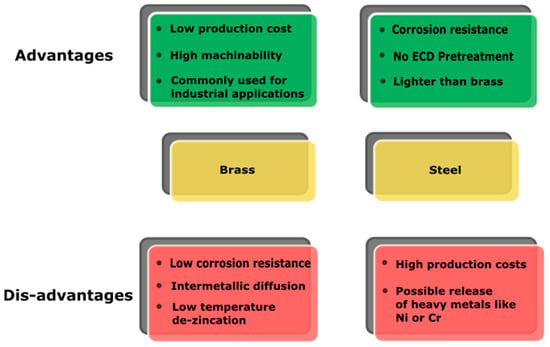
Regarding wearable artifacts, the release of heavy metals is a fundamental parameter for ensuring the quality and safety of the product for the customer. Common hazardous metals in wearable PVD-coated artifacts are nickel and lead. Although lead and nickel thin films can be deposited by PVD [
212,
213], those coatings are not of interest for decorative applications, but both could be found in small quantities inside substrate alloys. Nickel-containing steel is the most used type of steel for PVD applications and lead is added to brass to increase its machinability [
214], even if the trend is to employ new performing lead-free brasses [
91]. In addition, as we mentioned before, electroplated nickel is widely used as a strike layer for PVD topcoats if brass is used as a substrate. Nickel is considered a hazardous element for human health and its issues concerning human health are well reported in the literature [
215,
216]; the most common problem related to nickel-containing wearable objects is nickel allergy [
217]. Nickel-release tests have to be carried out according to EN 12472:2020 [
218], which regulates methods that simulate the wear and corrosion of artifacts for the detection of nickel release; nickel determination is regulated under EN 1811:2015 [
219] and an accurate report of the techniques used to quantify nickel release in decorative industries was accomplished by Giurlani [
95]. Lead needs to be considered one of the most important toxic heavy metals in the environment, and its full spectrum toxicity is reported in a 2015 review by Wani [
220]; in the European Union, lead percentage in alloys is regulated by the European Chemical Agency (ECHA) and only alloys with lead content of a weight lower than 0.05% are admitted in jewelry. Other important regulations are the US standard ASTM F2999-19 [
221] for adult’s jewelry, which sets a 1.5% threshold for lead in alloys, and the US standard ASTM F2923-14 [
222] for children’s jewelry, which sets the threshold at 0.01% [
223]. Determination of lead content in a sample is regulated under CPSC-CH-E1001-08.3 [
224], ISO 26482:2010 [
225], and EPA 6010C:2014 [
226].