Your browser does not fully support modern features. Please upgrade for a smoother experience.

Submitted Successfully!
Thank you for your contribution! You can also upload a video entry or images related to this topic.
For video creation, please contact our Academic Video Service.
| Version | Summary | Created by | Modification | Content Size | Created at | Operation |
|---|---|---|---|---|---|---|
| 1 | Guo hai yun | -- | 1705 | 2023-08-17 13:21:01 | | | |
| 2 | Rita Xu | + 257 word(s) | 1962 | 2023-08-18 03:16:50 | | | | |
| 3 | Rita Xu | + 3 word(s) | 1965 | 2023-08-21 10:27:14 | | |
Video Upload Options
We provide professional Academic Video Service to translate complex research into visually appealing presentations. Would you like to try it?
Cite
If you have any further questions, please contact Encyclopedia Editorial Office.
Zhang, Y.; Guo, H.; Cao, J.; Wu, X.; Jia, H.; Chang, A. Palladium-Plated Copper Bonding Wire. Encyclopedia. Available online: https://encyclopedia.pub/entry/48167 (accessed on 01 May 2026).
Zhang Y, Guo H, Cao J, Wu X, Jia H, Chang A. Palladium-Plated Copper Bonding Wire. Encyclopedia. Available at: https://encyclopedia.pub/entry/48167. Accessed May 01, 2026.
Zhang, Yuemin, Haiyun Guo, Jun Cao, Xuefeng Wu, Hewei Jia, Andong Chang. "Palladium-Plated Copper Bonding Wire" Encyclopedia, https://encyclopedia.pub/entry/48167 (accessed May 01, 2026).
Zhang, Y., Guo, H., Cao, J., Wu, X., Jia, H., & Chang, A. (2023, August 17). Palladium-Plated Copper Bonding Wire. In Encyclopedia. https://encyclopedia.pub/entry/48167
Zhang, Yuemin, et al. "Palladium-Plated Copper Bonding Wire." Encyclopedia. Web. 17 August, 2023.
Copy Citation
Wire-bonding technology is the most commonly used chip interconnection technology in microelectronic packaging. Metal bonding wire is the key material for wire bonding and plays an important role in the reliability of electronic devices. Palladium-plated copper (PdCu) bonding wire has been widely used because of its low cost, good electrical and thermal conductivity, the fact that it is not easy to oxidize, and its high reliability.
microelectronic packaging
Preparation of PdCu wire
distribution of Pd
1. Introduction
In microelectronic packaging, wire bonding is the most widely used and mature technology, which plays an important role in the performance of electronic devices, and metal-bonding wire is the key material of wire bonding. Gold-bonding wires have been dominant for a long time in the past, but in recent years, with the continuous rise of gold prices, it is urgent to find an alternative bonding wire with a lower cost. Copper (Cu) wire is becoming a standard wire-bonding material to replace gold wire in the semiconductor industry [1][2][3][4], especially in nanoelectronic packaging, because of its low price, excellent electrical and thermal conductivity, good strength and toughness, short heat-affected zone, and low necking failure rate [5][6][7][8][9].
However, the Cu wire has the following limitations in use: (1) oxidation of the wire surface; (2) the storage life before bonding; (3) stitch bondability; (4) the problem of increasing the cost of using mixed gas; (5) and long-term reliability. These problems limit the use of thin Cu wires in large-scale integration (LSI) packaging [10][11]. For example, using the Cu wire that has been oxidized on the surface for testing will cause the Cu ball to deviate from the ball in the burning ball, thereby reducing the bonding strength and affecting the reliability of the Cu wire.
Therefore, it is urgent to find a way to avoid Cu wire oxidation, prolong its storage life, and improve the reliability of Cu wire bonding. According to the literature, four kinds of metal thin coatings of Au, Ag, Pd, and Ni can prevent the oxidation of Cu wire [12][13][14]. The formation of spherical and high-quality free air ball (FAB) is the key requirement for the success of copper wire bonding. The melting point of Au and Ag is lower than that of Cu, and sharp balls will be formed during ball burning; Pd and Ni are precious metals, and their melting points are higher than that of Cu. However, it is found that the Ni-coated copper wire will form an eccentric ball during the burning of the ball. Only when Pd is plated can a good ball be formed [15][16]. Moreover, Pd has good ductility and plasticity, good adhesion to copper wire, a stable performance, and a high corrosion resistance in high-temperature and high-humidity environments [17]. These advantages of Pd promote the birth of PdCu wires. Pd coating not only solves the shortcomings of easy oxidation and high hardness of the Cu wire [18], but also prolongs its shelf life, broadens the bonding window of the second solder joint, and improves corrosion resistance and reliability [19][20][21][22][23][24]. Therefore, palladium-coated copper (PdCu) wire has been widely used in IC packaging, audio and video transmission lines, and other electronic devices.
The reliability of the PdCu wire is closely related to the quality of the Pd layer, the distribution position of Pd in FAB and the bonding interface, the growth of intermetallic compounds (IMCs), and the relationship between these three aspects is related to each other. The uniform and dense Pd layer on the surface of the Cu wire contributes to the relatively uniform distribution of Pd in FAB and the bonding interface. Pd slows down the growth of intermetallic compounds at the bonding interface, thereby improving the reliability of PdCu. How to obtain good Pd layer quality and then obtain PdCu wire with excellent performance, what are the factors affecting the distribution of Pd in FAB and the bonding interface, and what is the growth process and rate of Cu-Al intermetallic compounds in PdCu wire, these are the research hotspots in microelectronics packaging, and many scholars have conducted in-depth research on this.
2. Preparation of Palladium-Plated Copper (PdCu) Wire
At present, the preparation of PdCu wire in China mainly adopts electroplating, electroless plating, and direct plating technology. Electroplating and electroless plating technology is the earliest application technology. The preparation of palladium-plated copper (PdCu) wire by electroplating and electroless plating technology will produce harmful substances and pollute the environment [25]. Direct plating is a new Pd plating technology developed by researchers in recent years. It is simple to operate and does not produce harmful substances. It can be called “green Pd plating technology”.
2.1. Electroplating
Electroplating is an important surface treatment technology. It uses electrochemical methods to process the surface of metal and non-metal products, so that various metal coatings can be obtained on the surface [26] to improve the corrosion resistance and oxidation resistance of materials. The plating solution is generally composed of metal salt, reducing agent, buffer and complexing agent, stabilizer, brightener, etc. The process parameters of electroplating mainly include pH value, temperature, time, and current density. At present, there are two kinds of palladium-plating solutions: ammonium salt type and phosphate type [27]. The preparation of PdCu wire by electroplating technology is to plate a thicker Pd layer on a thicker (Φ > 0.15 mm) Cu wire, and then to obtain the PdCu wire of the required specifications after drawing the PdCu wire, intermediate heat treatment, PdCu wire finished drawing, PdCu wire final annealing, PdCu wire test or rewinding, and other steps. However, due to the different plastic deformation properties of Cu and Pd during the drawing process, it is difficult to draw fine (Φ < 0.016 mm) PdCu wire [28]. Therefore, in some ultra-narrow spacing microelectronic packaging, it is difficult to prepare the required specifications of fine PdCu wire by electroplating technology, and the preparation process will produce harmful substances and pollute the environment. In the process of drawing, there may also be problems such as palladium layer shedding and uneven thickness of the palladium layer. Figure 1 shows the electroplating process [28].
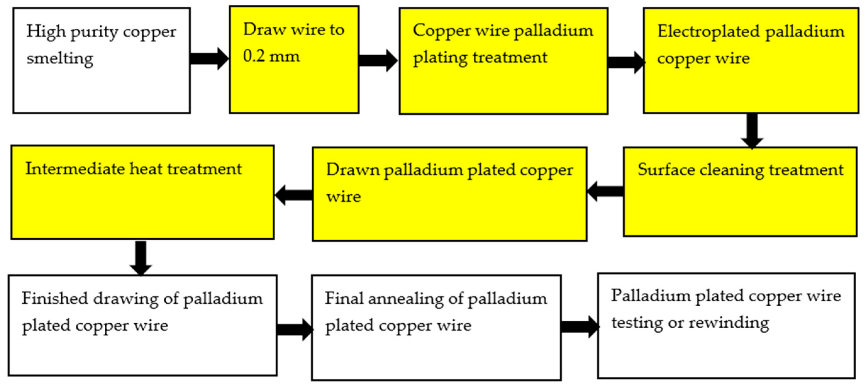
Figure 1. Palladium electroplating process for bonded copper wire.
2.2. Electroless Plating
Electroless plating is a plating method in which metal ions in the plating solution are reduced to metal and deposited on the surface of parts by means of a suitable reducing agent without impressed current. Electroless palladium plating can deposit palladium membrane with uniform thickness on the surface of the complex matrix. It is the most widely used method to prepare palladium membrane because of its low cost, simple equipment, easy operation, good uniformity, and compactness [29].
Zhou et al. [30] developed a chemical method for the preparation of PdCu wire and applied for an invention patent. This method uses copper with a mass percentage greater than 99.95%, and then completes the preparation by melting and drawing, electroless palladium plating before annealing of the finished product, annealing, cleaning, rewinding and other steps. Compared with the traditional PdCu wire, the performance of the PdCu wire obtained by this preparation method has been improved, and the production process is safe, energy-saving, and simple. Zhang et al. [31] first studied electroless palladium plating on the surface of copper sheet, and then analyzed that due to the difference in the surface area of copper wire and copper sheet, the activation energy of palladium deposition on the surface of copper wire was small. By increasing the concentration of isopropanolamine to control the growth of the palladium particles, the formula composition and process suitable for electroless palladium plating on copper wire were obtained: PdCl2 2 g/ L, NaH2PO2·H2O 12 g/L, 38% (mass fraction) HCl4 mL/L, 28% (mass fraction) NH3 H2O 160 mL/L, Bismuth nitrate 55 mg/L, auxiliary complexing agent isopropanolamine 35 mL/L pH 9.8, at a temperature of 52 °C and a duration of 35 min. The surface of the coating obtained by the formula composition and process is uniform and fine, and there is no delamination and crack, as shown in Figure 2.
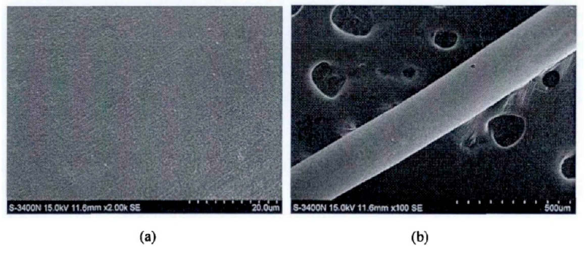
Figure 2. Surface morphology of palladium coating at different magnifications, (a): 2000 times and (b): 100 times.
PdCu wire is prepared by electroless plating. Although the production process has low cost, good uniformity, and compactness of the obtained palladium film, ultimately, the chemical solution is used, and the waste liquid will be produced in the preparation process, which will cause certain pollution to the environment and bring pressure to the ecological environment. The following focuses on a “green palladium plating process”.
2.3. Direct Plating
Direct palladium-plating technology, namely coating-palladium technology, is used to directly coat nano-palladium organic solution on the finished bonded copper wire, and deposit nano-palladium on the surface of copper wire by a heat-treatment process [28]. Therefore, the preparation of PdCu wire by direct-plating technology requires the preparation of PdCu wire blank line first, and then adjusting the coating process parameters, and finally obtaining the finished product.
Figure 3 shows the drawing process. The 6 N copper was drawn into 8 mm single-crystal copper rod in a single-crystal continuous casting furnace, and then the single-crystal copper rod was drawn into copper bonding wires of different specifications after rough drawing, medium drawing, fine drawing, and micro wire drawing [32].
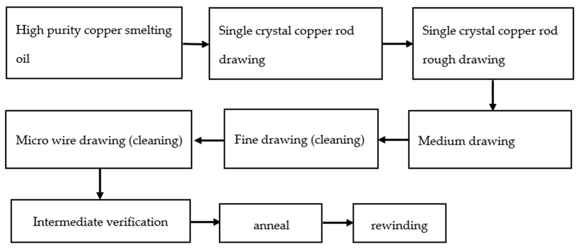
Figure 3. Bonded copper wire drawing process.
Direct palladium-plating process [33]: (1) mold cleaning; (2) prepare the copper wire to be coated and wear the mold; (3) absorb the coating liquid with a medical needle tube without a rubber head; (4) according to the diameter of copper wire and the thickness of palladium layer, the speed of the bidirectional pump is set, and the bidirectional pump is opened; (5) when the speed of the pump reaches a predetermined value, start coating; (6) observe the coating color and adjust the temperature and speed appropriately. The coating schematic is shown in Figure 4.
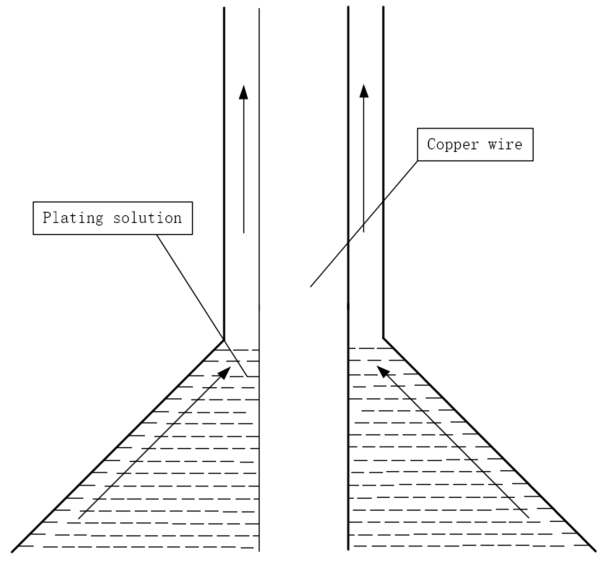
Figure 4. Coating schematic.
The principle of direct palladium-plating technology [34]: Firstly, by adding various chemical substances, the nano ultrafine powder is uniformly dispersed and suspended in the plating solution, and the plating solution has high wettability and stability. The surfactant in the plating solution is coated around the nanoparticles, and the dispersion between the nanoparticles is realized by the steric hindrance. Then, the drawn fine copper bonding wire is immersed in a specially prepared solution containing nano-metal powder. By drying the heating device and optimizing the heating deposition process parameters, a smooth and flat coating can be formed on the surface of the copper bonding wire. The effect of drying is to volatilize or decompose the solvent and other organic substances in the solution, leaving only the pure coating to adhere to the surface of the copper wire. Under the action of heat treatment, the coating completes the sintering process and is accompanied by grain growth and interface diffusion, thus forming a surface nano-coating with high interfacial bonding strength and brightness. The schematic diagram and device of surface nano-coating are shown in Figure 5 and Figure 6, respectively [34].
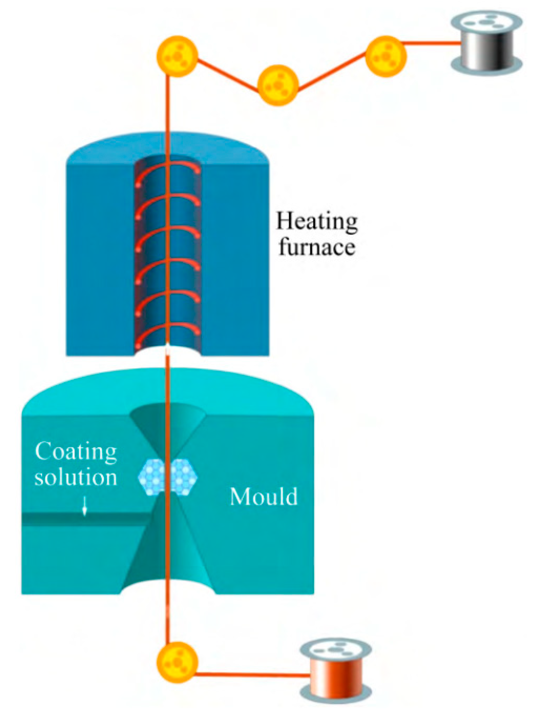
Figure 5. Principle of surface nano-coating process.
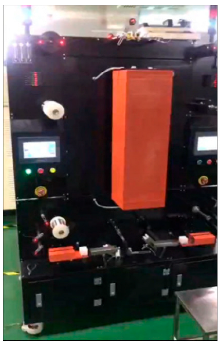
Figure 6. Nano-coating device for micro wire surface.
The PdCu wire prepared by direct plating has good chemical stability, no cracking and peeling, excellent bonding performance, uniform coating, and a dense structure. Compared with electroplating and electroless plating, direct plating has the advantages of a simple process, low costs (approximately 11% of electroplating and electroless plating), environmental protection in the production process, no harmful substances, and a smooth and uniform coating surface [25][33]. From Figure 7, it can be seen that the surface quality of directly-plated palladium copper wire is better than that of electroplating and electroless plating. Therefore, in general, the performance (fracture force, elongation, etc.) of directly-plated palladium copper wire will be better than that of electroplating and electroless plating.

Figure 7. Comparison of surface morphology of PdCu wire.
In summary, the fine copper bonding wire can be prepared by direct palladium-plating technology, and the prepared fine copper bonding wire has a good performance, stable chemical properties, a uniform palladium layer, and a good density. Direct palladium-plating technology is not only simple, but also produces no harmful substances in the preparation process, does not pollute the air and land, and is superior to electroplating and electroless plating.
References
- Zhong, Z.W. Overview of wire bonding using copper wire or insulated wire. Microelectron. Reliab. 2011, 51, 4–12.
- Charles, J.; Gunasekaran, M.; Malliah, R. Factors affecting the long-term stability of Cu/Al ball bonds subjected to standard and extended high temperature storage. Microelectron. Reliab. 2011, 51, 137–147.
- Qin, I.W.; Chylak, B.; Clauberg, H.; Shah, A.; Foley, J. Ball Bond Process Optimization with Cu and Pd-Coated Cu Wire. ECS Trans. 2012, 44, 891–901.
- Chauhan, P.S.; Choubey, A.; Zhong, Z.W.; Pecht, M.G. Copper Wire Bonding; Springer: Berlin/Heidelberg, Germany, 2014.
- Abdul, R.D.; Tan, C.W. Mechanical and Electrical Properties of Au-Al and Cu-Al Intermetallics Layer at Wire Bonding Interface. J. Electron. Packag. 2003, 125, 617–620.
- Cho, J.-H.; Rollett, A.D.; Cho, J.-S.; Papk, Y.-J.; Moon, J.-T.; OH, K.H. Investigation of recrystallization and grain growth of copper and gold bonding wires. Metall. Mater. Trans. A 2006, 37, 3085–3097.
- Schneider-Ramelow, M.; Ehrhardt, C. The reliability of wire bonding using Ag and Al. Microelectron. Reliab. 2016, 63, 336–341.
- Nguyen, L.T.; Mcdonald, D. Optimization of copper wire bonding on Al-Cu metallization. IEEE Trans. Compon. Packag. Manuf. Technol. 1995, 18, 423–429.
- Murali, S.; Srikanth, N.; Vath III, C.J. Grains, deformation substructures, and slip bands observed in thermosonic copper ball bonding. Mater. Charact. 2003, 50, 9–50.
- Uno, T. Bond reliability under humid environment for coated copper wire and bare copper wire. Microelectron. Reliab. 2011, 51, 148–156.
- Tan, C.W.; Daud, A.R.; Yarmo, M.A. Corrosion study at Cu–Al interface in microelectronics packaging. Appl. Surf. Sci. 2002, 191, 67–73.
- Kaimori, S.; Nonaka, T.; Mizoguchi, A. Development of ‘Hybrid Bonding Wire’. SEI Tech. Rev. 2006, 63, 14–18.
- Uno, T. Enhancing bondability with coated copper bonding wire. Microelectron. Reliab. 2011, 51, 88–96.
- Zhou, H.; Zhang, Y.; Cao, J.; Su, C.; Li, C.; Chang, A.; An, B. Research Progress on Bonding Wire for Microelectronic Packaging. Micromachines 2023, 14, 432.
- Kaimori, S.; Nonaka, T.; Mizoguchi, A. The Development of Cu Bonding Wire with Oxidation-Resistant Metal Coating. IEEE Trans. Adv. Packag. 2006, 29, 227–231.
- Cheng, P.-Y.; Lai, P.-Y.; Ye, Z.-J.; Hesieh, C.-L.; Ye, J.-M. Effect of Pd distribution on Pd-plated Cu wire using different electronic flame off settings. J. Mater. Sci. Mater. Electron. 2017, 28, 4613–4618.
- Qin, W.; Anderson, T.; Chang, G. Mechanism to improve the reliability of copper wire bonding with palladium-coating of the wire. Microelectron. Reliab. 2019, 99, 239–244.
- Koh, W.; Lee, T.K.; Ng, H.S.; Goh, K.S. Investigation of palladium coverage on bonded balls of palladium-coated copper wires. In Proceedings of the IEEE 2011 12th International Conference on Electronic Packaging Technology and High Density Packaging, Shanghai, China, 1 January 2011.
- Xu, H.; Qin, I.; Clauberg, H.; Chylak, B.; Acoff, V.L. Behavior of palladium and its impact on intermetallic growth in palladium-coated Cu wire bonding. Acta Mater. 2013, 61, 79–88.
- Stephan, D.; Chew, E.; Yeung, J.; Milke, E. Impact of palladium to the interfacial behavior of palladium coated copper wire on aluminium pad metallization during high temperature storage. In Proceedings of the IEEE 2011 IEEE 13th Electronics Packaging Technology Conference, Singapore, 7–9 December 2011.
- Uno, T.; Kimura, K.; Yamada, T. Surface-enhanced copper bonding wire for LSI and its bond reliability under humid environment. In Proceedings of the IEEE 2009 European Microelectronics and Packaging Conference, Rimini, Italy, 15–18 June 2009.
- England, L.; Eng, S.T.; Liew, C.; Lim, H.H. Cu wire bond parameter optimization on various bond pad metallization and barrier layer material schemes. Microelectron. Reliab. 2010, 51, 81–87.
- Gam, S.-A.; Kim, H.-J.; Cho, J.-S.; Park, Y.-J.; Moon, J.-T.; Paik, K.-W. Effects of Cu and Pd Addition on Au Bonding Wire/Al Pad Interfacial Reactions and Bond Reliability. J. Electron. Mater. 2006, 35, 2048–2055.
- Gan, C.L.; Hashim, U. Reliability Assessment and Activation Energy Study of Au and Pd-Coated Cu Wires Post High Temperature Aging in Nanoscale Semiconductor Packaging. J. Electron. Packag. 2013, 135, 210101–210107.
- Kong, Y.N. The Research on Manufacturing Process and Properties of Palladium Coated Copper Wire. Master’s Thesis, Lanzhou University of Technology, Lanzhou, China, 2013.
- Cao, R.-P.; Xiao, S.-M. Study on Technology of Palladium Plating. Surf. Technol. 2004, 33, 50–51.
- Kang, F.F.; Yang, G.X.; Kong, J.W.; Dao, P.; Wu, Y.J.; Zhang, K.H. The Development Trend of Palladium–plated Bonding Copper Wire. Mater. Rev. 2011, 25, 104–107, 128.
- Cao, J.; Fan, J.L.; Gao, W.B. Investigation of copper direct coating Pd technology and bonding properties. Mater. Sci. Technol. 2015, 23, 110–114.
- Zhang, T.-T.; Zhao, L.-L.; Wan, C.-Y.; He, Y.-Q.; Xu, B. Study on process of electroless palladium plating on copper. Electroplat. Finish. 2015, 34, 1100–1104.
- Zhou, X.G.; Du, L.M.; Xiang, C.H.; Su, H.F.; Chen, B. A Chemically Plated Palladium Copper Bonding Wire and Its Preparation Method. China Patent CN103560120B, 3 March 2016.
- Zhang, T.-T. Improvement of Stability of Copper Wire Bonding. Master’s Thesis, Shanghai Institute of Technology, Shanghai, China, 2016.
- Ding, Y.-T.; Cao, J.; Hu, Y.; Kou, S.-Z.; Xu, G.-J. Study on Effect Factor for Preparation Process of Single Crystal Copper Bonding Wire. Foundry Technol. 2007, 28, 1648–1651.
- Ding, Y.T.; Kong, Y.N.; Cao, J.; Hu, Y.; Sun, G. Research on Producing Process and Performance of Pd-coated Copper Wire. Foundry Technol. 2013, 34, 142–145.
- Song, K.-X.; Zhou, Y.-J.; Mi, X.-J.; Xiao, Z.; Cao, J.; Ding, Y.-T.; Wu, B.-A.; Feng, C.-L.; Li, Z.; Chen, D.-B.; et al. Preparation, microstructure and properties of copper based wire. Trans. Nonferrous Met. Soc. China 2020, 30, 2845–2874.
More
Information
Subjects:
Materials Science, Coatings & Films
Contributors
MDPI registered users' name will be linked to their SciProfiles pages. To register with us, please refer to https://encyclopedia.pub/register
:
View Times:
2.3K
Revisions:
3 times
(View History)
Update Date:
21 Aug 2023
Notice
You are not a member of the advisory board for this topic. If you want to update advisory board member profile, please contact office@encyclopedia.pub.
OK
Confirm
Only members of the Encyclopedia advisory board for this topic are allowed to note entries. Would you like to become an advisory board member of the Encyclopedia?
Yes
No
${ textCharacter }/${ maxCharacter }
Submit
Cancel
Back
Comments
${ item }
|
More
No more~
There is no comment~
${ textCharacter }/${ maxCharacter }
Submit
Cancel
${ selectedItem.replyTextCharacter }/${ selectedItem.replyMaxCharacter }
Submit
Cancel
Confirm
Are you sure to Delete?
Yes
No


