Your browser does not fully support modern features. Please upgrade for a smoother experience.
Please note this is an old version of this entry, which may differ significantly from the current revision.
Subjects:
Materials Science, Coatings & Films
引线键合技术是微电子封装中最常用的芯片互连技术。金属键合线是引线键合的关键材料,对电子设备的可靠性起着重要作用。镀钯铜(PdCu)键合丝因其成本低、导电导热性好、不易氧化、可靠性高等特点而得到广泛应用。
- microelectronic packaging
- Preparation of PdCu wire
1. Introduction
In microelectronic packaging, wire bonding is the most widely used and mature technology, which plays an important role in the performance of electronic devices, and metal-bonding wire is the key material of wire bonding. Gold-bonding wires have been dominant for a long time in the past, but in recent years, with the continuous rise of gold prices, it is urgent to find an alternative bonding wire with a lower cost. Copper (Cu) wire is becoming a standard wire-bonding material to replace gold wire in the semiconductor industry [1,2,3,4], especially in nanoelectronic packaging, because of its low price, excellent electrical and thermal conductivity, good strength and toughness, short heat-affected zone, and low necking failure rate [5,6,7,8,9].
However, the Cu wire has the following limitations in use: (1) oxidation of the wire surface; (2) the storage life before bonding; (3) stitch bondability; (4) the problem of increasing the cost of using mixed gas; (5) and long-term reliability. These problems limit the use of thin Cu wires in large-scale integration (LSI) packaging [10,11]. For example, using the Cu wire that has been oxidized on the surface for testing will cause the Cu ball to deviate from the ball in the burning ball, thereby reducing the bonding strength and affecting the reliability of the Cu wire.
Therefore, it is urgent to find a way to avoid Cu wire oxidation, prolong its storage life, and improve the reliability of Cu wire bonding. According to the literature, four kinds of metal thin coatings of Au, Ag, Pd, and Ni can prevent the oxidation of Cu wire [12,13,14]. The formation of spherical and high-quality free air ball (FAB) is the key requirement for the success of copper wire bonding. The melting point of Au and Ag is lower than that of Cu, and sharp balls will be formed during ball burning; Pd and Ni are precious metals, and their melting points are higher than that of Cu. However, it is found that the Ni-coated copper wire will form an eccentric ball during the burning of the ball. Only when Pd is plated can a good ball be formed [15,16]. Moreover, Pd has good ductility and plasticity, good adhesion to copper wire, a stable performance, and a high corrosion resistance in high-temperature and high-humidity environments [17]. These advantages of Pd promote the birth of PdCu wires. Pd coating not only solves the shortcomings of easy oxidation and high hardness of the Cu wire [18], but also prolongs its shelf life, broadens the bonding window of the second solder joint, and improves corrosion resistance and reliability [19,20,21,22,23,24]. Therefore, palladium-coated copper (PdCu) wire has been widely used in IC packaging, audio and video transmission lines, and other electronic devices.
The reliability of the PdCu wire is closely related to the quality of the Pd layer, the distribution position of Pd in FAB and the bonding interface, the growth of intermetallic compounds (IMCs), and the relationship between these three aspects is related to each other. The uniform and dense Pd layer on the surface of the Cu wire contributes to the relatively uniform distribution of Pd in FAB and the bonding interface. Pd slows down the growth of intermetallic compounds at the bonding interface, thereby improving the reliability of PdCu. How to obtain good Pd layer quality and then obtain PdCu wire with excellent performance, what are the factors affecting the distribution of Pd in FAB and the bonding interface, and what is the growth process and rate of Cu-Al intermetallic compounds in PdCu wire, these are the research hotspots in microelectronics packaging, and many scholars have conducted in-depth research on this.
2. Preparation of Palladium-Plated Copper (PdCu) Wire
At present, the preparation of PdCu wire in China mainly adopts electroplating, electroless plating, and direct plating technology. Electroplating and electroless plating technology is the earliest application technology. The preparation of palladium-plated copper (PdCu) wire by electroplating and electroless plating technology will produce harmful substances and pollute the environment [25]. Direct plating is a new Pd plating technology developed by researchers in recent years. It is simple to operate and does not produce harmful substances. It can be called “green Pd plating technology”.
2.1. Electroplating
Electroplating is an important surface treatment technology. It uses electrochemical methods to process the surface of metal and non-metal products, so that various metal coatings can be obtained on the surface [26] to improve the corrosion resistance and oxidation resistance of materials. The plating solution is generally composed of metal salt, reducing agent, buffer and complexing agent, stabilizer, brightener, etc. The process parameters of electroplating mainly include pH value, temperature, time, and current density. At present, there are two kinds of palladium-plating solutions: ammonium salt type and phosphate type [27]. The preparation of PdCu wire by electroplating technology is to plate a thicker Pd layer on a thicker (Φ > 0.15 mm) Cu wire, and then to obtain the PdCu wire of the required specifications after drawing the PdCu wire, intermediate heat treatment, PdCu wire finished drawing, PdCu wire final annealing, PdCu wire test or rewinding, and other steps. However, due to the different plastic deformation properties of Cu and Pd during the drawing process, it is difficult to draw fine (Φ < 0.016 mm) PdCu wire [28]. Therefore, in some ultra-narrow spacing microelectronic packaging, it is difficult to prepare the required specifications of fine PdCu wire by electroplating technology, and the preparation process will produce harmful substances and pollute the environment. In the process of drawing, there may also be problems such as palladium layer shedding and uneven thickness of the palladium layer. Figure 1 shows the electroplating process [28].
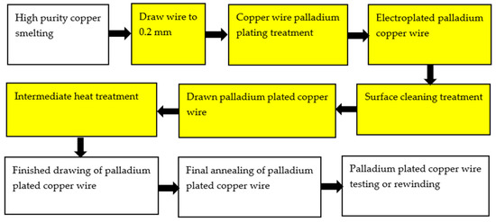
Figure 1. Palladium electroplating process for bonded copper wire.
2.2. Electroless Plating
Electroless plating is a plating method in which metal ions in the plating solution are reduced to metal and deposited on the surface of parts by means of a suitable reducing agent without impressed current. Electroless palladium plating can deposit palladium membrane with uniform thickness on the surface of the complex matrix. It is the most widely used method to prepare palladium membrane because of its low cost, simple equipment, easy operation, good uniformity, and compactness [29].
Zhou et al. [30] developed a chemical method for the preparation of PdCu wire and applied for an invention patent. This method uses copper with a mass percentage greater than 99.95%, and then completes the preparation by melting and drawing, electroless palladium plating before annealing of the finished product, annealing, cleaning, rewinding and other steps. Compared with the traditional PdCu wire, the performance of the PdCu wire obtained by this preparation method has been improved, and the production process is safe, energy-saving, and simple. Zhang et al. [31] first studied electroless palladium plating on the surface of copper sheet, and then analyzed that due to the difference in the surface area of copper wire and copper sheet, the activation energy of palladium deposition on the surface of copper wire was small. By increasing the concentration of isopropanolamine to control the growth of the palladium particles, the formula composition and process suitable for electroless palladium plating on copper wire were obtained: PdCl2 2 g/ L, NaH2PO2·H2O 12 g/L, 38% (mass fraction) HCl4 mL/L, 28% (mass fraction) NH3 H2O 160 mL/L, Bismuth nitrate 55 mg/L, auxiliary complexing agent isopropanolamine 35 mL/L pH 9.8, at a temperature of 52 °C and a duration of 35 min. The surface of the coating obtained by the formula composition and process is uniform and fine, and there is no delamination and crack, as shown in Figure 2.
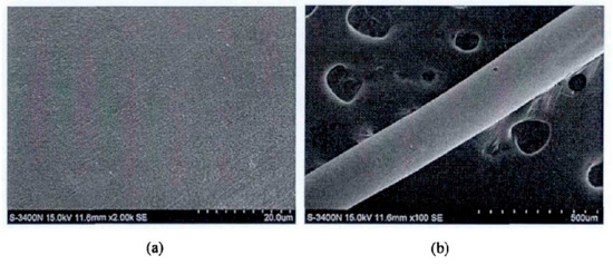
Figure 2. Surface morphology of palladium coating at different magnifications, (a): 2000 times and (b): 100 times.
PdCu wire is prepared by electroless plating. Although the production process has low cost, good uniformity, and compactness of the obtained palladium film, ultimately, the chemical solution is used, and the waste liquid will be produced in the preparation process, which will cause certain pollution to the environment and bring pressure to the ecological environment. The following focuses on a “green palladium plating process”.
2.3. Direct Plating
Direct palladium-plating technology, namely coating-palladium technology, is used to directly coat nano-palladium organic solution on the finished bonded copper wire, and deposit nano-palladium on the surface of copper wire by a heat-treatment process [28]. Therefore, the preparation of PdCu wire by direct-plating technology requires the preparation of PdCu wire blank line first, and then adjusting the coating process parameters, and finally obtaining the finished product.
Figure 3 shows the drawing process. The 6 N copper was drawn into 8 mm single-crystal copper rod in a single-crystal continuous casting furnace, and then the single-crystal copper rod was drawn into copper bonding wires of different specifications after rough drawing, medium drawing, fine drawing, and micro wire drawing [32].
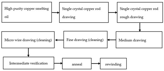
Figure 3. Bonded copper wire drawing process.
Direct palladium-plating process [33]: (1) mold cleaning; (2) prepare the copper wire to be coated and wear the mold; (3) absorb the coating liquid with a medical needle tube without a rubber head; (4) according to the diameter of copper wire and the thickness of palladium layer, the speed of the bidirectional pump is set, and the bidirectional pump is opened; (5) when the speed of the pump reaches a predetermined value, start coating; (6) observe the coating color and adjust the temperature and speed appropriately. The coating schematic is shown in Figure 4.
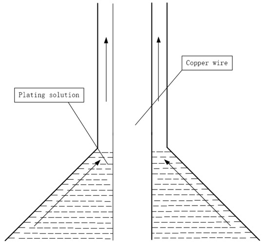
Figure 4. Coating schematic.
The principle of direct palladium-plating technology [34]: Firstly, by adding various chemical substances, the nano ultrafine powder is uniformly dispersed and suspended in the plating solution, and the plating solution has high wettability and stability. The surfactant in the plating solution is coated around the nanoparticles, and the dispersion between the nanoparticles is realized by the steric hindrance. Then, the drawn fine copper bonding wire is immersed in a specially prepared solution containing nano-metal powder. By drying the heating device and optimizing the heating deposition process parameters, a smooth and flat coating can be formed on the surface of the copper bonding wire. The effect of drying is to volatilize or decompose the solvent and other organic substances in the solution, leaving only the pure coating to adhere to the surface of the copper wire. Under the action of heat treatment, the coating completes the sintering process and is accompanied by grain growth and interface diffusion, thus forming a surface nano-coating with high interfacial bonding strength and brightness. The schematic diagram and device of surface nano-coating are shown in Figure 5 and Figure 6, respectively [34].
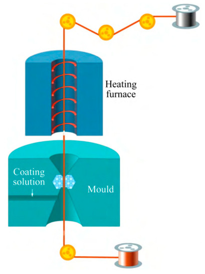
Figure 5. Principle of surface nano-coating process.
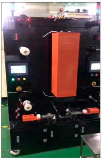
图6.用于微线表面的纳米涂层装置。
直接电镀制备的PdCu线具有良好的化学稳定性,不开裂和剥落,粘接性能优异,涂层均匀,结构致密。与电镀和化学镀相比,直接电镀具有工艺简单、成本低(约为电镀和化学镀的11%)、生产过程中环保、无有害物质、涂层表面光滑均匀等优点[25,33]。从图7可以看出,直镀钯铜线的表面质量优于电镀和化学镀。所以, 一般来说, 直接电镀钯铜线的性能(断裂力, 伸长率, 等)会优于电镀和化学镀.
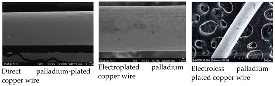
图7.PdCu线表面形貌的比较。
综上所述,采用直接镀钯技术可制备细铜键合丝,制备的细铜键合丝性能好,化学性能稳定,钯层均匀,密度好。直接镀钯技术不仅简单,而且在制备过程中不产生有害物质,不污染空气和土地,优于电镀和化学镀。
This entry is adapted from the peer-reviewed paper 10.3390/mi14081538
This entry is offline, you can click here to edit this entry!