Submitted Successfully!
To reward your contribution, here is a gift for you: A free trial for our video production service.
Thank you for your contribution! You can also upload a video entry or images related to this topic.
Version Summary Created by Modification Content Size Created at Operation
1 -- 2095 2023-06-26 18:44:22 |
2 Format correct Meta information modification 2095 2023-06-27 07:43:14 |

Video Upload Options

Do you have a full video?

Confirm

Are you sure to Delete?
Cite
If you have any further questions, please contact Encyclopedia Editorial Office.
Fang, W.; Li, Q.; Li, J.; Li, Y.; Zhang, Q.; Chen, R.; Wang, M.; Yun, F.; Wang, T. Deep Ultraviolet Photodetectors Based on Aluminum Nitride Material. Encyclopedia. Available online: https://encyclopedia.pub/entry/46074 (accessed on 27 July 2024).
Fang W, Li Q, Li J, Li Y, Zhang Q, Chen R, et al. Deep Ultraviolet Photodetectors Based on Aluminum Nitride Material. Encyclopedia. Available at: https://encyclopedia.pub/entry/46074. Accessed July 27, 2024.
Fang, Wannian, Qiang Li, Jiaxing Li, Yuxuan Li, Qifan Zhang, Ransheng Chen, Mingdi Wang, Feng Yun, Tao Wang. "Deep Ultraviolet Photodetectors Based on Aluminum Nitride Material" Encyclopedia, https://encyclopedia.pub/entry/46074 (accessed July 27, 2024).
Fang, W., Li, Q., Li, J., Li, Y., Zhang, Q., Chen, R., Wang, M., Yun, F., & Wang, T. (2023, June 26). Deep Ultraviolet Photodetectors Based on Aluminum Nitride Material. In Encyclopedia. https://encyclopedia.pub/entry/46074
Fang, Wannian, et al. "Deep Ultraviolet Photodetectors Based on Aluminum Nitride Material." Encyclopedia. Web. 26 June, 2023.
Deep Ultraviolet Photodetectors Based on Aluminum Nitride Material
Edit

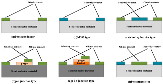
Photodetectors are important photoelectric devices that realize sensing detection through photoelectric signal transformation and have been widely used in flame sensing, conversion communication, environmental monitoring, video imaging, night vision imaging, military tracking, medical detection, and other fields. Ultraviolet with a wavelength less than 280 nm is defined as a deep ultraviolet band that will be absorbed by ozone in the atmosphere before entering the earth. Almost no signal background exists in this band on the earth, which is also called a solar-blind band. The application fields represented by ultraviolet short-range secure communication, shipborne guidance, ozone layer monitoring, and water pollution treatment need the continuous development, maturity, transformation, and application of deep ultraviolet (DUV) detection technology. Therefore, further research and development of DUV detection technology have attracted the extensive attention of researchers in relevant fields, whether in daily life or in the construction of modern national defense.

aluminum nitride photodetectors nanowires semiconductor deep ultraviolet

1. Introduction

Photodetectors can generally be divided into the following types: photoconductive detectors, photovoltaic detectors, and phototransistors [1][2]. These types of detectors are based on different operating principles and have their own advantages. Basic photoconductive detectors are formed by using the photoconductive material as the channel and placing the metal with Ohmic contact as the electrode at both ends of the channel. Additionally, there is often a light gain mechanism, that is, a type of charge carrier that can cycle through the external circuit many times before recombining the carrier with the opposite charge type, resulting in an increase in photocurrent and a decrease in response speed [1]. Photovoltaic detectors mainly include MSM type, Schottky barrier type, and p-n (p-i-n) junction type [3]. MSM detectors are made up of double “back-to-back” semiconductor Schottky barriers by using an interdigitated electrode with planar linearity on top of an active light collection region. When under DC bias, one of the Schottky barriers will be forward biased and the other reverse biased, so the dark current is quite small. Due to the low capacitance per unit area and limited transit time, MSM photodiodes also have an intrinsic rapid response ability. Schottky detectors consist of a semitransparent Schottky contact and an Ohmic contact and have many advantages, such as high responsivity, high quantum efficiency, low dark current, short response time, and possible zero-bias operations. The p-n (p-i-n) junction type shares some similarities with Schottky photodiodes in that both devices exploit the photovoltaic effect. When forward bias is applied in the p-n junction, the dark current is far greater than the photocurrent, and the detector is unable to work due to unilateral conductivity characteristics. Under reverse bias, the dark current is suppressed, and moreover, the carrier transit time and diode capacitance are reduced, which is beneficial to the improvement of sensitivity [4][5]. Phototransistors are special photoconductive detectors that separate the photoconductive material of the detector from the grid with a thin dielectric layer. The applied grid voltage can adjust the carrier density through the field effect and can make the dark current of the device in the “off” state [6][7]. The schematic structure of these devices is illustrated in Figure 1.
Figure 1. Schematic structure of the different types of wide-bandgap semiconductor UV detectors: (a) Photoconductor; (b) MSM type; (c) Schottky barrier type; (d) p-n junction type; (e) p-i-n junction type; (f) Phototransistor.
The first synthesis of aluminum nitride (AlN) by reaction of nitrogen and molten aluminum can be traced back to 1862 [8], which did not receive much attention at that time. Since the 1960s, researchers have been committed to the growth of AlN single crystals [9][10]. As important III-V semiconductors, AlN exhibits high thermal conductivity (K~3.19 Wcm−1K−1), high melting point (>2300 °C), and large direct bandgap (6.28 eV) [11].

2. AlN Nanostructures

Nanomaterials with a large surface-to-volume ratio and higher sensitivity have attracted attention in the photosensitive device application field. In recent years, UV photodetectors based on AlN nanostructures, especially nanowires, have been paid much attention, including photoconductors [12][13][14], MSM photodetectors [15][16], and Schottky photodiodes [17].
Liu et al. successfully prepared ultralong AlN nanowire (UAN) arrays using the CVD method [12]. Individual ultralong AlN nanowires showed significant photoconductive effects under different excited lights, which was attributed to the dominant molecular sensitization effects, as shown in Figure 2a. It was found that they had a much faster response speed of 1 ms, a higher photocurrent response of 2.7 × 10⁶, and a more reproductive working performance in the air environment (Figure 2b,c). Teker fabricated a single-AlN nanowire DUV photodetector via high-quality AlN nanowires fabricated by the dielectrophoretic assembly method [14]. The DUV photodetector showed a high photocurrent response to the 254 nm UV light under a low operating voltage (≤3 V), with rise and decay time constants of 7.7 s and 11.5 s, respectively.
Figure 2. (a) Illustration of the photosensitive mechanisms of single UANs. (b) I–V curves of a single UAN at an irradiance of 0.6 μW/cm2. (c). Time response of a photocurrent at different light intensities under 325 nm light [12]. (d) SEM images of AlN micro/nanowires. (e) Schematic description of the photodetector. (f) Photoresponse spectrum under different wavelengths. Inset: dark current as function of voltage [15].
From the research results of Zheng et al., high-quality AlN micro/nanowires were grown by a two-step physical vapor transport method, the SEM images of which are shown in Figure 2d [15]. Figure 2e depicts the schematic diagram of a vacuum ultraviolet (VUV) detector fabricated by these micro/nanowires. From the response spectrum in Figure 2f, an ultrashort cutoff wavelength of 193 nm was found in this VUV photodetector. In addition, the fast photoresponse speed (<0.1 s) and recovery time (<0.2 s) were obtained. Ali et al. fabricated a flexible UV photodetector based on AlN nanowire networks via a low-cost non-lithographic fabrication scheme [16]. The detector exhibited a good photocurrent response at 2 V bias, a very fast photoresponse rise time of 0.27 s, and a decay time of 0.41 s to UV light.
Yusuf et al. reported a highly responsive, flexible AlN single-nanowire ultraviolet photodetector [17]. Through a scalable and highly cost-efficient hot-contact method, detection arrays of very small-size devices capable of operating at 0 V and 30 V were achieved. The responsivity, excellent EQE, and detectivity of the detector were 1197.5 mA/W, 584%, and 2.32 × 10¹²  Jones under 254 nm UV light exposure at 30 V bias.

3. AlN Thin Films

With the development of semiconductor technology, many methods for growing AlN crystals have been developed, mainly including physical vapor transport (PVT) [18][19][20], chemical vapor deposition (CVD) [21][22][23], molecular beam epitaxy (MBE) [24], pulsed laser deposition (PLD) [25][26], and magnetron sputtering [27][28]. The common substrate materials used for epitaxial growth of AlN crystals mainly include Si, SiC [20], sapphire, etc.
At present, the research based on AlN film detectors is mainly focused on the MSM type [29][30][31][32][33][34]. For instance, Chen et al. deposited AlN thin films directly on c-plane sapphire substrates [29]. According to the evaluation of atomic force microscope, the films showed a smooth surface with a root mean square (RMS) roughness as small as 0.7 nm, and the spectral response of MSM photodetectors constructed with AlN/sapphire revealed peak responsivity at 200 nm and a UV/visible rejection ratio about 102. Using the hydride vapor phase epitaxial (HVPE) technique, Murtaza et al. successfully deposited 200 nm thick AlN films onto an n-type silicon wafer [30]. Electrical and electro-optic characterization was conducted on different circuit configurations of AlN/silicon under various biases and temperatures, and it was found that reverse-biased silicon coupled with the interdigitated AlN scheme can provide the maximum response rate in photovoltaic and photoconductive modes.
Conventional MSM UV detectors have the shortcomings of a long carrier path, a finite electrical field, and difficult-to-adjust structural parameters. Li et al. demonstrated a 3D-MSM structural AlN-based DUV detector [33]. Compared with conventional MSM devices, 3D-MSM devices exhibited higher responsiveness and response speed. The enhanced performance was to be attributed to the intensified electrical field from the 3D metal electrode configuration and the inhibition of the carrier vertical transport, which unambiguously increased the carrier collection efficiency and migration speed. After that, the same group investigated the effect of asymmetric electrode materials (Figure 3a–c) on MSM device performance [32], and the Ni-Al device had better responsivity. Without applied voltage, a photoelectric response current increased from a dark current of 2.6 pA to 10 nA after UV illumination.
Figure 3. (a) Sketch of the asymmetric MSM device. Time-dependent photoresponse under 8 V bias for UV on and off (b), and responsivity (c) for different electrodes with Ni−Ni, Al−Al, and Ni−Al [32]. (d) Process of obtaining a self-assembled monolayer on an AlN epitaxial film. (e) Variation of dark current. (f) Photo-to-dark current ratio (PDCR) with voltage before and after surface modification [34].
AlN was plagued with a large density of electronic surface states about 1013 to 1014 eV−1 cm−2.5, which modified the current transport mechanisms and led to a large leakage current in the device [35]. Kaushik et al. used ZnTPP(OH) for passivation of the electronic surface states of AlN, forming a self-assembled monolayer, as shown in Figure 3d [34]. The surface modification of AlN effectively reduced the dark current of the photodetector without deteriorating the photocurrent. Based on the surface-modified AlN photodetector, the ratio of photocurrent to dark current was enhanced from 930 to 7835 at −2 V, and the responsivity doubled from 0.3 to 0.6 mA/W at 5 V (Figure 3e,f).

4. AlN Heterostructures

AlN has been combined with a AlGaN film for DUV photodiode application [36]. DUV photodetectors based on AlN/AlGaN heterostructures grown on sapphire by MOCVD offered good performance at a wavelength of 240 nm. A simple-structure n-AlGaN/AlN phototransistor with a self-depleted full channel was reported, which was implemented by utilizing the strong polarization-induced electric field as a virtual photogate [37]. The complete depletion of the n-Al0.5Ga0.5N channel layer and the high optical gain of 1.3 × 10⁵ resulted in a very low dark current of 1.7 pA and a high photo-to-dark current ratio of 108 (Figure 4a,b). In addition, an ultrahigh responsivity of 1.6 × 10⁵ A/W and an ultrafast response speed of 537.5 ps were obtained (Figure 4c). AlN can combine with Ga2O3 as a lateral heterojunction in order to perform solar-blind photodetection [38]. Under zero-bias conditions, the dark current, UV light switching ratio, linear dynamic region, photoresponsivity, specific detectivity, and rise and decay time were 1.45 × 10⁻¹³ A, 2.14 × 10⁴, 86.74 dB, 95.95 μA W−1, 5.98 × 10¹⁰ Jones, and 90/116 ms, respectively. The heterojunction with a staggered type-II band alignment was established successfully, which could be self-powered because of the built-in electric field formation. High-quality AlN films via the MOCVD technique were prepared by Li et al. [39], as shown in Figure 4d. A p-graphene/i-AlN/n-GaN photovoltaic far ultraviolet (FUV) detector was constructed, and Figure 4e shows the I-V characteristics of the device under 185 nm light and dark conditions, which indicates that there was an open-circuit voltage of ~1.15 V and an ultrahigh switching ratio at different voltages. The high responsivity of 25 mA/W and the sharp cutoff edge at 206 nm of the device are shown in Figure 4f.
Figure 4. Dark and illuminated I–V curves of the n-Al0.5Ga0.5N/AlN photodetectors with different channel layer: (a) 70 nm and (b) 100 nm. (c) Spectral responses at different bias voltages of the FCSD phototransistor [37]. (d) Brightfield cross-sectional TEM images of AlN/GaN heterojunctions. (e) I−V characteristic of the devices under dark conditions and 185 nm light of 30.6 µW/cm2. (f) Spectral responsivity (Rλ) curves of PDs illuminated by different-wavelength light. Inset: Rλ−λ curve in logarithmic coordinates [39].
To conclude, AlN has obtained good response results in the DUV shortwave region due to the ultrawide bandgap. However, the responsivity of detectors based on AlN thin films is generally low, at the level of mA W−1. The responsivity of AlN micro/nanowires is higher than films due to their small body–surface ratio. AlN materials usually form heterojunctions photodetectors with AlGaN and GaN. These devices have excellent performance in dark current, on/off ratio, responsivity, and response speed, and have great development potential. Table 1 summarizes the performance parameters of AlN-based DUV photodetectors.
Table 1. Summary of performance parameters of DUV photodetectors based on AlN.
Device Structure Fabrication Method Light of Detection/nm Dark Current On/Off Ratio Rejection Ratio Specific Detectivity/Jones EQE Responsivity Rise Time/
Decay Time
Ref.
AlN nanowire
photoconductor
CVD 325   20       2.7 × 10⁶ A/W
@40 V
~1 ms [12]
AlN nanowire
photoconductor
LPCVD 254             7.7 s/
11.5 s
[14]
AlN
micro/nanowire
MSM
PVT 190 <100 fA@20 V   VUV/UV-C
~104
  254 0.39 A/W
@50 V
<0.1 s/
<0.2 s
[15]
AlN nanowire
MSM
LPCVD 254           2.43 mA/W
@15 V
0.27 s/
0.41 s
[16]
AlN nanowire
Schottky
LPCVD 254       2.32 × 10¹²  584 1187.5 mA/W@30 V   [17]
AlN film
3D-MSM
MOCVD 200 2.6 pA         1.51 mA/W
@0 V
  [32]
AlN film
3D-MSM
MOCVD 200 4.2 pA@8 V         8 mA/W@2 V 2.61 ns/
3 ns
[33]
AlN film
FC-3DMSM
MOCVD 200 5.96 pA@8 V         9.6 mA/W
@2 V
2.90 ns/
2.92 ns
[33]
AlN film
MSM
PVD 200 14.6 pA@5 V 7835@−2 V       0.6 mA/W
@5 V
0.9 s/
1.8 s
[34]
AlN/AlGaN Heterostructures
MSM
MOCVD 240 10 pA@20 V             [36]
AlN/AlGaN HeterostructuresTFT LP-MOCVD 240 1.7 pA@20 V >108 240/280
>102
1.5 × 10¹⁸
@20 V
  1.6 × 10⁵ A/W
@20 V
537.5 ps
3.1 us
[37]
Ga2O3/AlN heterojunction
p-n
sputter 253 0.145 pA 2.14 × 10⁴   5.98 × 10¹⁰   95.95 μA/W
@0 V
90 ms/
116 ms
[38]
Gr/AlN/GaN Heterostructures
p-i-n
MOCVD 194     194/212
>103
  16 25 mA/W
@0 V
  [39]

References

  1. Xie, C.; Lu, X.; Tong, X.; Zhang, Z.; Liang, F.; Liang, L.; Luo, L.; Wu, Y. Recent Progress in Solar-Blind Deep-Ultraviolet Photodetectors Based on Inorganic Ultrawide Bandgap Semiconductors. Adv. Funct. Mater. 2019, 29, 1806006.
  2. Shang, H.; Dai, M.; Gao, F.; Yang, H.; Hu, P.; Jia, D.; Zhou, Y.; Chen, H. Progress in Inorganic Ultraviolet Photoelectric Materials. Mater. China 2019, 38, 875–886.
  3. Feng, W.; Jin, Z.; Yuan, J.; Zhang, J.; Jia, S.; Dong, L.; Yoon, J.; Zhou, L.; Vajtai, R.; Tour, J.M.; et al. A fast and zero-biased photodetector based on GaTe-InSe vertical 2D p-n heterojunction. 2D Mater. 2018, 5, 025008.
  4. Dai, M.; Chen, H.; Feng, R.; Feng, W.; Hu, Y.; Yang, H.; Liu, G.; Chen, X.; Zhang, J.; Xu, C.-Y.; et al. A Dual-Band Multilayer InSe Self-Powered Photodetector with High Performance Induced by Surface Plasmon Resonance and Asymmetric Schottky Junction. ACS Nano 2018, 12, 8739–8747.
  5. Zou, Y.; Zhang, Y.; Hu, Y.; Gu, H. Ultraviolet Detectors Based on Wide Bandgap Semiconductor Nanowire: A Review. Sensors 2018, 18, 2072.
  6. Feng, W.; Zheng, W.; Cao, W.; Hu, P. Back Gated Multilayer InSe Transistors with Enhanced Carrier Mobilities via the Suppression of Carrier Scattering from a Dielectric Interface. Adv. Mater. 2014, 26, 6587–6593.
  7. Lu, Y.-J.; Lin, C.-N.; Shan, C.-X. Optoelectronic Diamond: Growth, Properties, and Photodetection Applications. Adv. Opt. Mater. 2018, 6, 1800359.
  8. Briegleb, F.; Geuther, A. Ueber das Stickstoffmagnesium und die Affinitäten des Stickgases zu Metallen. Eur. J. Org. Chem. 1862, 123, 228–241.
  9. Taylor, K.M.; Lenie, C. Some Properties of Aluminum Nitride. J. Electrochem. Soc. 1960, 107, 308.
  10. Cox, G.; Cummins, D.; Kawabe, K.; Tredgold, R. On the preparation, optical properties and electrical behaviour of aluminium nitride. J. Phys. Chem. Solids 1967, 28, 543–548.
  11. Alaie, Z.; Nejad, S.M.; Yousefi, M. Recent advances in ultraviolet photodetectors. Mater. Sci. Semicond. Process. 2015, 29, 16–55.
  12. Liu, F.; Li, L.; Guo, T.; Gan, H.; Mo, X.; Chen, J.; Deng, S.; Xu, N. Investigation on the photoconductive behaviors of an individual AlN nanowire under different excited lights. Nanoscale Res. Lett. 2012, 7, 454.
  13. Kenry; Yong, K.T.; Yu, S.F. AlN nanowires: Synthesis, physical properties, and nanoelectronics applications. J. Mater. Sci. 2012, 47, 5341–5360.
  14. Teker, K. Dielectrophoretic Assembly of Aluminum Nitride (AlN) Single Nanowire Deep Ultraviolet Photodetector. J. Nano Res. 2019, 60, 86–93.
  15. Zheng, W.; Huang, F.; Zheng, R.; Wu, H. Low-Dimensional Structure Vacuum-Ultraviolet-Sensitive (λ < 200 nm) Photodetector with Fast-Response Speed Based on High-Quality AlN Micro/Nanowire. Adv. Mater. 2015, 27, 3921–3927.
  16. Ali, Y.A.; Teker, K. Fabrication of ultraviolet photodetector with aluminum nitride nanowire networks via direct transfer method. Microelectron. Eng. 2019, 211, 26–28.
  17. Ozdemir, Y.B.; Teker, K.; Yildirim, M.A. High-responsivity flexible ultraviolet photodetector via single aluminum nitride nanowire. Opt. Eng. 2021, 60, 057104.
  18. Hartmann, C.; Wollweber, J.; Dittmar, A.; Irmscher, K.; Kwasniewski, A.; Langhans, F.; Neugut, T.; Bickermann, M. Preparation of Bulk AlN Seeds by Spontaneous Nucleation of Freestanding Crystals. Jpn. J. Appl. Phys. 2013, 52, 08JA06.
  19. Wang, Q.; Lei, D.; He, G.; Gong, J.; Huang, J.; Wu, J. Characterization of 60 mm AlN Single Crystal Wafers Grown by the Physical Vapor Transport Method. Phys. Status Solidi 2019, 216, 1900118.
  20. Hu, W.; Guo, L.; Guo, Y.; Wang, W. Growing AlN crystals on SiC seeds: Effects of growth temperature and seed orientation. J. Cryst. Growth 2020, 541, 125654.
  21. Knauer, A.; Mogilatenko, A.; Hagedorn, S.; Enslin, J.; Wernicke, T.; Kneissl, M.; Weyers, M. Correlation of sapphire off-cut and reduction of defect density in MOVPE grown AlN. Phys. Status Solidi 2016, 253, 809–813.
  22. Claudel, A.; Blanquet, E.; Chaussende, D.; Audier, M.; Pique, D.; Pons, M. Thermodynamic and experimental investigations on the growth of thick aluminum nitride layers by high temperature CVD. J. Cryst. Growth 2009, 311, 3371–3379.
  23. Kumagai, Y.; Kubota, Y.; Nagashima, T.; Kinoshita, T.; Dalmau, R.; Schlesser, R.; Moody, B.; Xie, J.; Murakami, H.; Koukitu, A.; et al. Preparation of a Freestanding AlN Substrate from a Thick AlN Layer Grown by Hydride Vapor Phase Epitaxy on a Bulk AlN Substrate Prepared by Physical Vapor Transport. Appl. Phys. Express 2012, 5, 055504.
  24. Mansurov, V.; Nikitin, A.; Galitsyn, Y.; Svitasheva, S.; Zhuravlev, K.; Osvath, Z.; Dobos, L.; Horvath, Z.; Pecz, B. AlN growth on sapphire substrate by ammonia MBE. J. Cryst. Growth 2007, 300, 145–150.
  25. Shukla, G.; Khare, A. Dependence of N2 pressure on the crystal structure and surface quality of AlN thin films deposited via pulsed laser deposition technique at room temperature. Appl. Surf. Sci. 2008, 255, 2057–2062.
  26. Szekeres, A.; Fogarassy, Z.; Petrik, P.; Vlaikova, E.; Cziraki, A.; Socol, G.; Ristoscu, C.; Grigorescu, S.; Mihailescu, I. Structural characterization of AlN films synthesized by pulsed laser deposition. Appl. Surf. Sci. 2011, 257, 5370–5374.
  27. Li, T.; Han, J.; Xing, Y.; Deng, X.; Li, J.; Zhang, L.; Shi, F.; Yu, L.; Sun, C.; Zhang, X.; et al. Influence of pressure on the properties of AlN deposited by DC reactive magnetron sputtering on Si (100) substrate. Micro Nano Lett. 2019, 14, 146–149.
  28. Xiao, S.; Suzuki, R.; Miyake, H.; Harada, S.; Ujihara, T. Improvement mechanism of sputtered AlN films by high-temperature annealing. J. Cryst. Growth 2018, 502, 41–44.
  29. Chen, M.-R.; Chen, H.-G.; Kao, H.-L.; Wu, M.-G.; Tzou, A.-J.; Chen, J.S.; Chou, H. Structural and optical properties of low temperature grown AlN films on sapphire using helicon sputtering system. J. Vac. Sci. Technol. A 2015, 33, 031503.
  30. Murtaza, S.H.; Ahmed, S.; Ali, M. Investigation of AlN/Si based heterogeneous Junction using inter-digitated electrodes for enhanced UV light detection. Optik 2022, 265, 169534.
  31. Yang, R.Y.; Hsiung, C.M.; Chen, H.H.; Wu, H.W.; Shih, M.C. Effect of AlN film thickness on photo/dark currents of MSM UV photodetector. Microw. Opt. Technol. Lett. 2008, 50, 2863–2866.
  32. Li, T.; Song, W.; Zhang, L.; Yan, J.; Zhu, W.; Wang, L. Self-powered asymmetric metal–semiconductor–metal AlN deep ultraviolet detector. Opt. Lett. 2022, 47, 637–640.
  33. Li, T.; Long, L.; Hu, Z.; Wan, R.; Gong, X.; Zhang, L.; Yuan, Y.; Yan, J.; Zhu, W.; Wang, L.; et al. Three-dimensional metal–semiconductor–metal AlN deep-ultraviolet detector. Opt. Lett. 2020, 45, 3325–3328.
  34. Kaushik, S.; Naik, T.R.; Alka, A.; Garg, M.; Tak, B.R.; Ravikanth, M.; Rao, V.R.; Singh, R. Surface Modification of AlN Using Organic Molecular Layer for Improved Deep UV Photodetector Performance. ACS Appl. Electron. Mater. 2020, 2, 739–746.
  35. Eller, B.S.; Yang, J.; Nemanich, R.J. Electronic surface and dielectric interface states on GaN and AlGaN. J. Vac. Sci. Technol. A 2013, 31, 050807.
  36. Averin, S.V.; Kuznetsov, P.I.; Zhitov, V.A.; Alkeev, N.V.; Kotov, V.M.; Dorofeev, A.A.; Gladysheva, N.B. AlN/AlGaN heterostructures for selective ultraviolet MSM detectors. Tech. Phys. 2011, 56, 295–297.
  37. Lu, J.; Lv, Z.; Qiu, X.; Lai, S.; Jiang, H. Ultrasensitive and high-speed AlGaN/AlN solar-blind ultraviolet photodetector: A full-channel-self-depleted phototransistor by a virtual photogate. Photon Res. 2022, 10, 2229.
  38. Hao, Y.; Wang, X.; An, Y. A Ga2O3/AlN heterojunction for self-powered solar-blind photodetection with high photo-to-dark current ratio and fast response speed. Phys. Scr. 2021, 96, 125835.
  39. Li, T.; Lu, Y.; Chen, Z. Heteroepitaxy Growth and Characterization of High-Quality AlN Films for Far-Ultraviolet Photodetection. Nanomaterials 2022, 12, 4169.
More
Information
Contributors MDPI registered users' name will be linked to their SciProfiles pages. To register with us, please refer to https://encyclopedia.pub/register : , , , , , , , ,
View Times: 259
Revisions: 2 times (View History)
Update Date: 27 Jun 2023
1000/1000
Video Production Service