Submitted Successfully!
To reward your contribution, here is a gift for you: A free trial for our video production service.
Thank you for your contribution! You can also upload a video entry or images related to this topic.
Version Summary Created by Modification Content Size Created at Operation
1 -- 5888 2023-05-25 16:24:41 |
2 format correct Meta information modification 5888 2023-05-26 02:20:52 |

Video Upload Options

Do you have a full video?

Confirm

Are you sure to Delete?
Cite
If you have any further questions, please contact Encyclopedia Editorial Office.
Jamaatisomarin, F.; Chen, R.; Hosseini-Zavareh, S.; Lei, S. High-Performance Laser Scribing of Thin Film Solar Cells. Encyclopedia. Available online: https://encyclopedia.pub/entry/44853 (accessed on 03 September 2024).
Jamaatisomarin F, Chen R, Hosseini-Zavareh S, Lei S. High-Performance Laser Scribing of Thin Film Solar Cells. Encyclopedia. Available at: https://encyclopedia.pub/entry/44853. Accessed September 03, 2024.
Jamaatisomarin, Farzad, Ruqi Chen, Sajed Hosseini-Zavareh, Shuting Lei. "High-Performance Laser Scribing of Thin Film Solar Cells" Encyclopedia, https://encyclopedia.pub/entry/44853 (accessed September 03, 2024).
Jamaatisomarin, F., Chen, R., Hosseini-Zavareh, S., & Lei, S. (2023, May 25). High-Performance Laser Scribing of Thin Film Solar Cells. In Encyclopedia. https://encyclopedia.pub/entry/44853
Jamaatisomarin, Farzad, et al. "High-Performance Laser Scribing of Thin Film Solar Cells." Encyclopedia. Web. 25 May, 2023.
High-Performance Laser Scribing of Thin Film Solar Cells
Edit

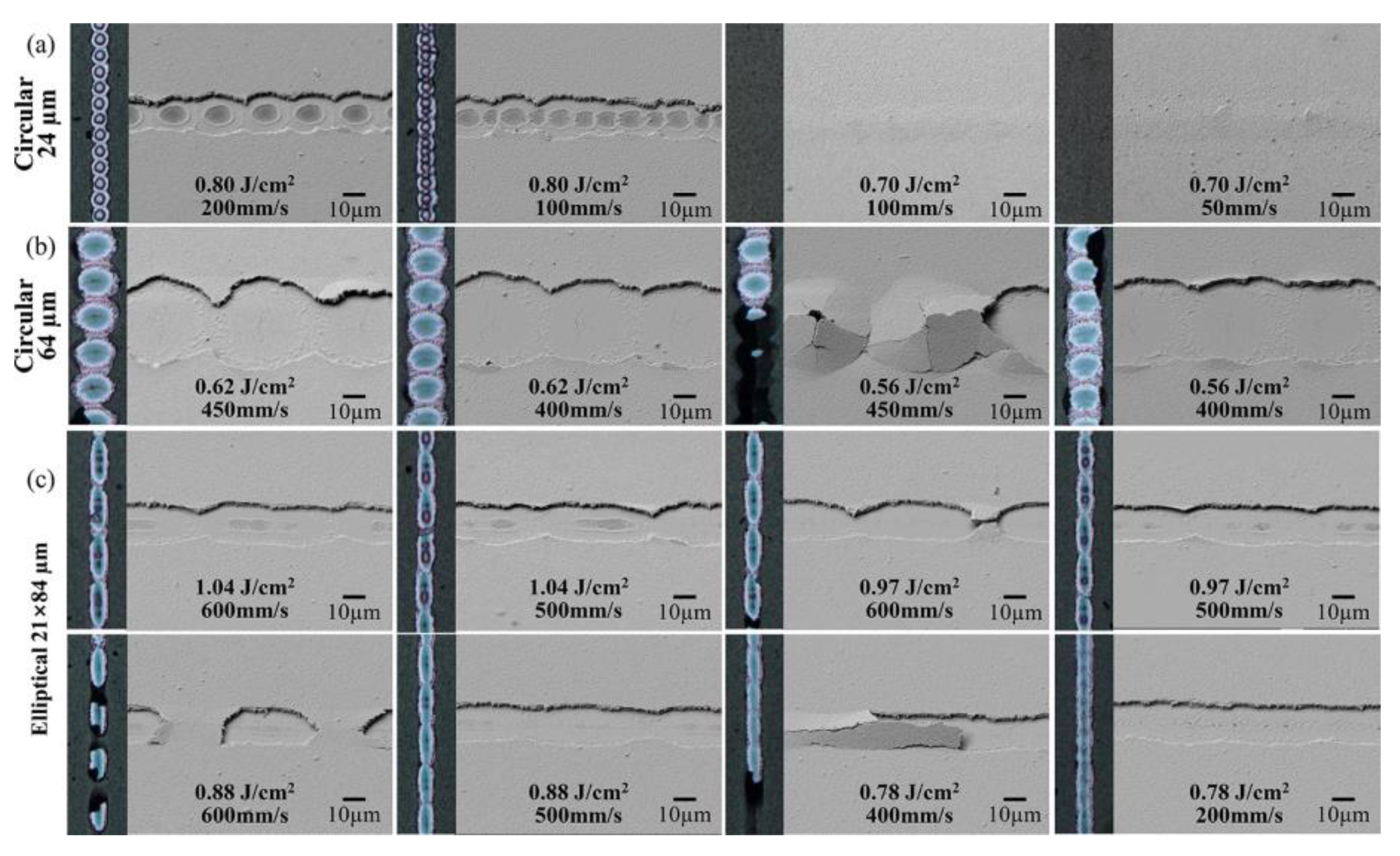
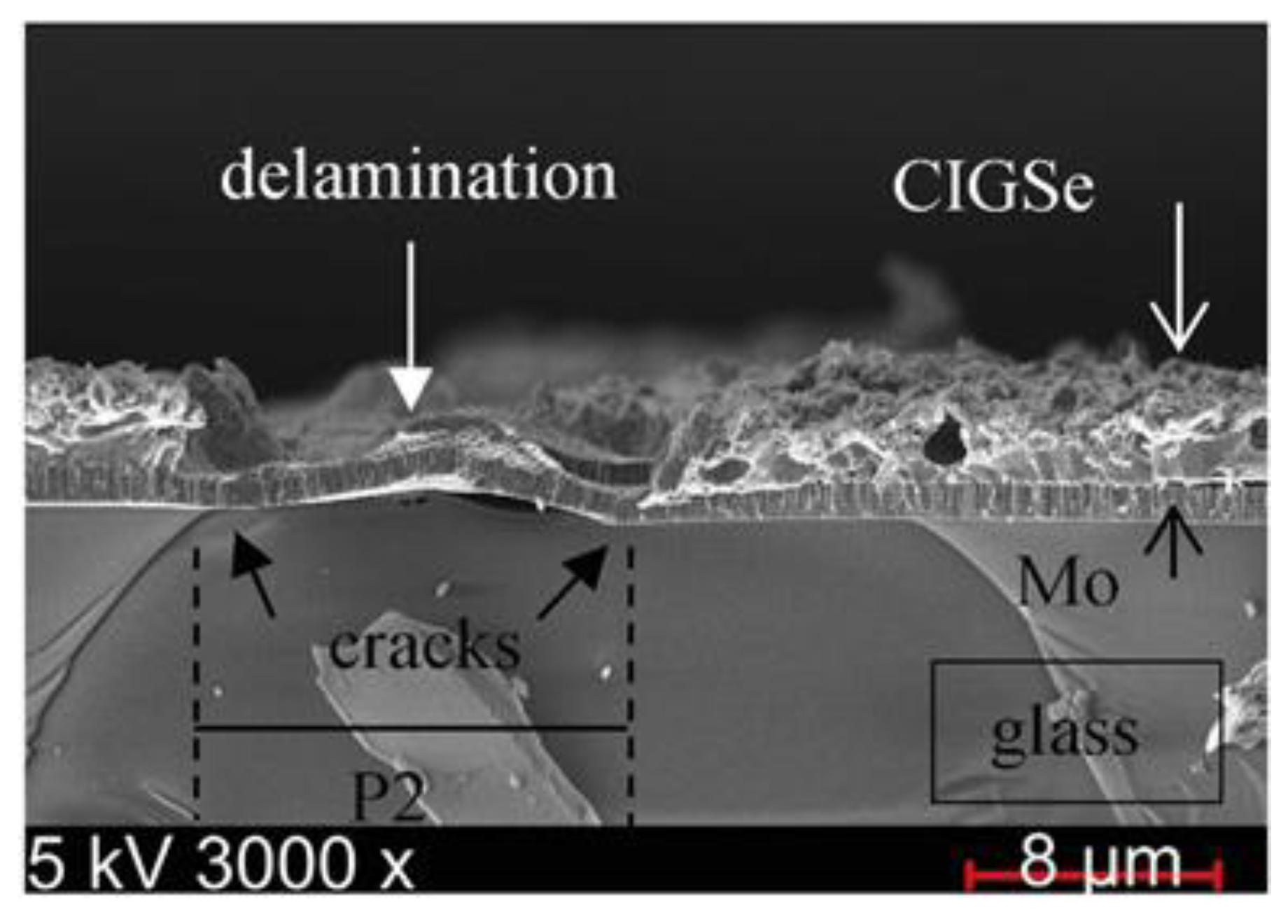
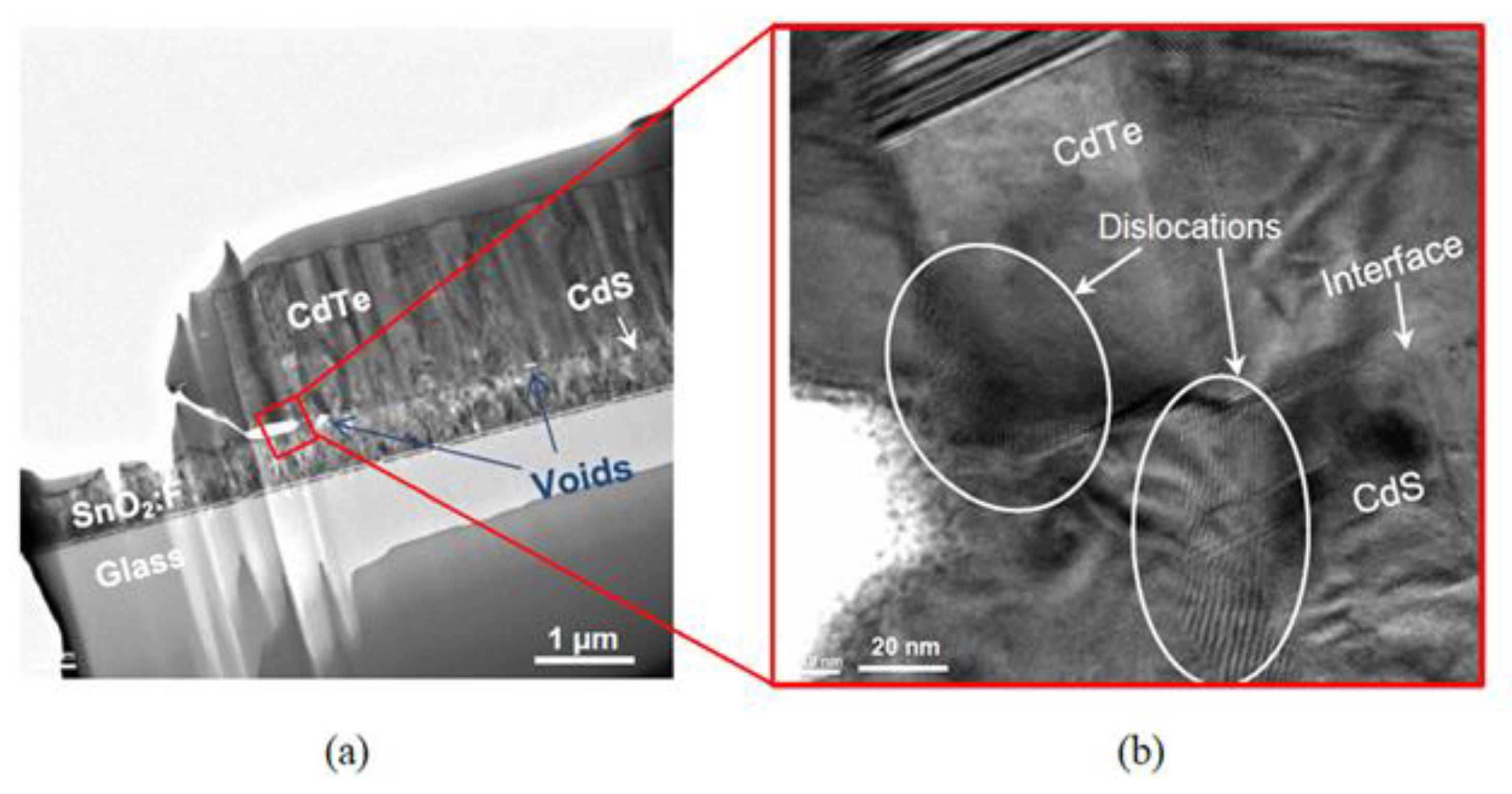
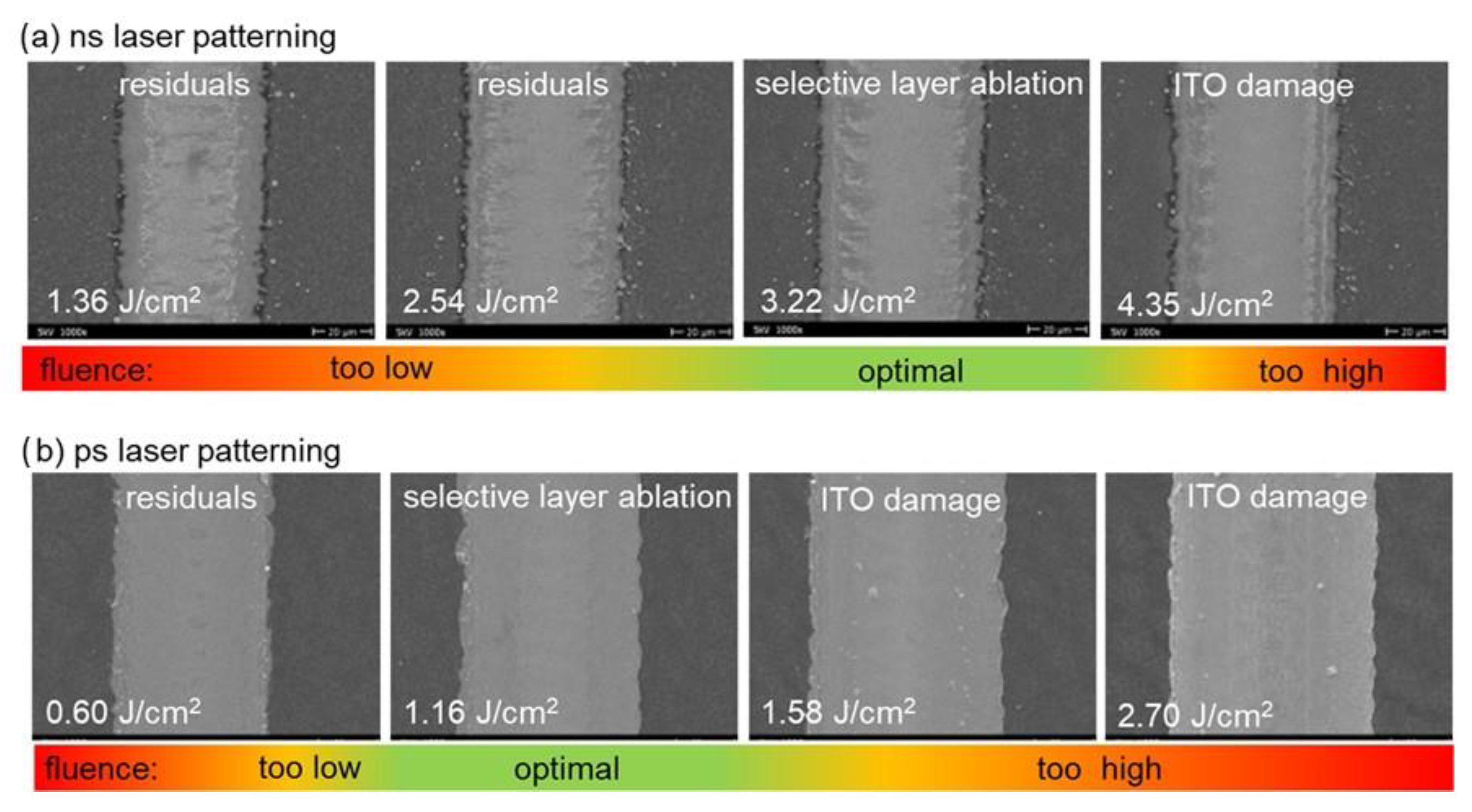
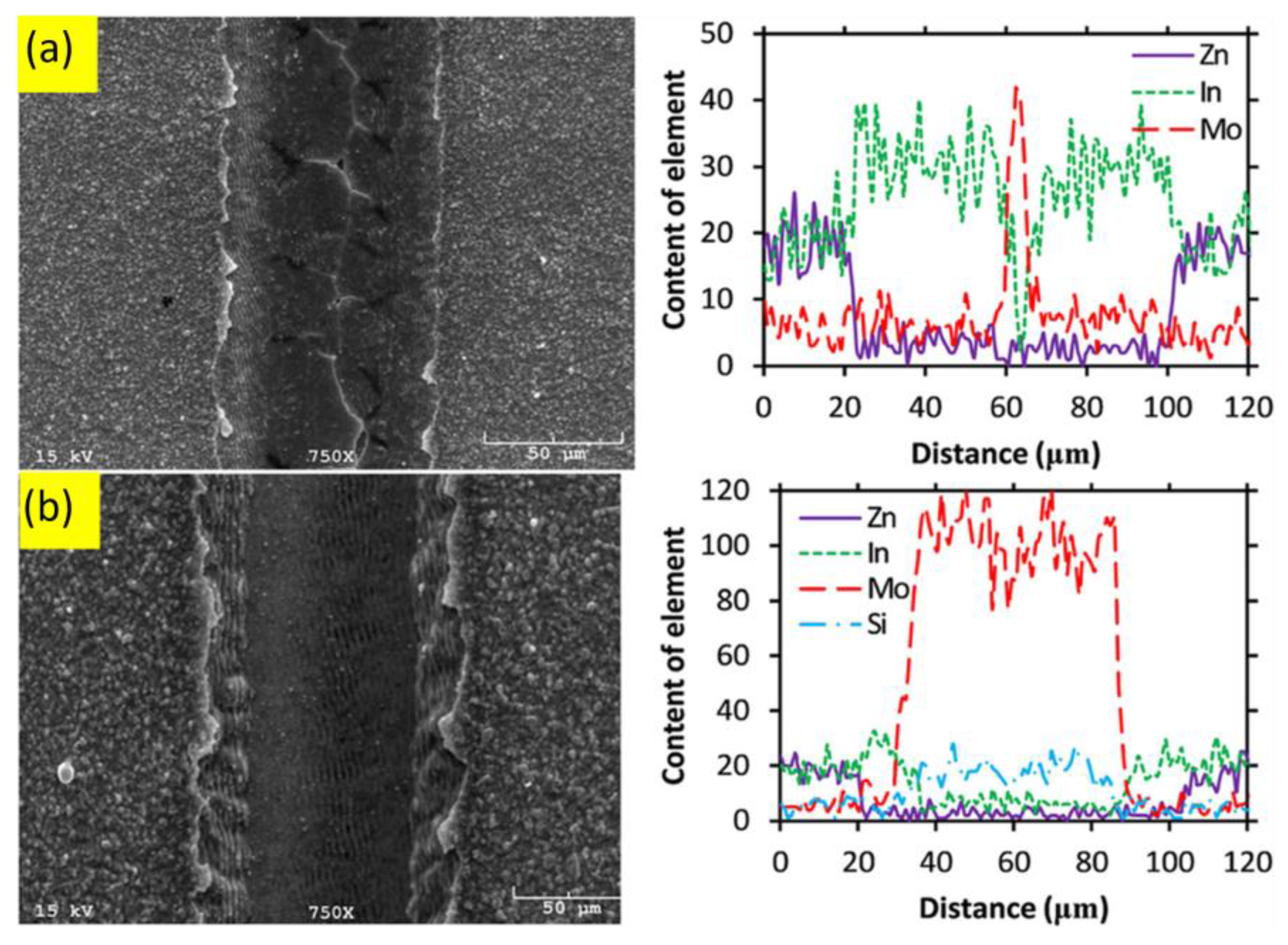
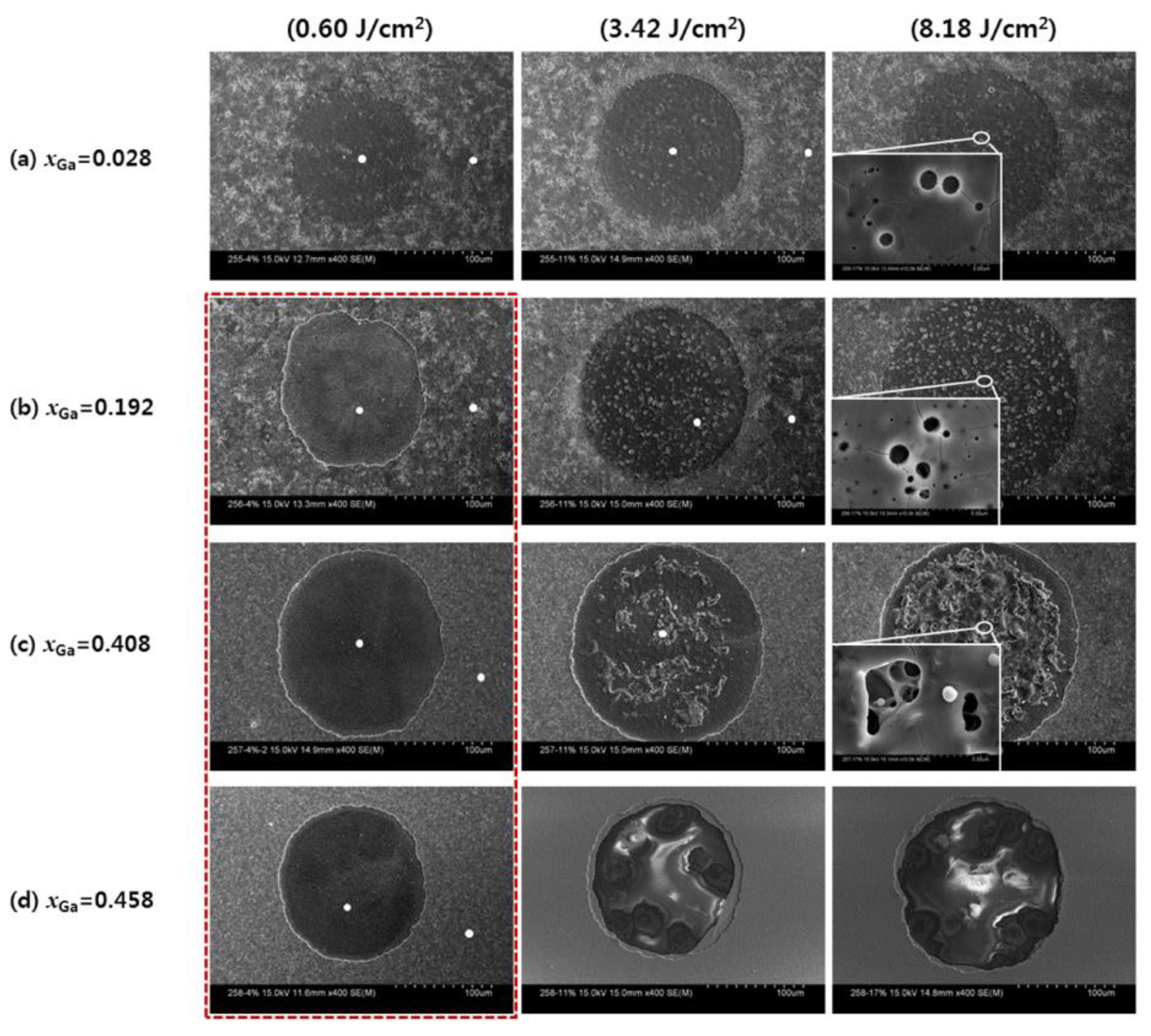
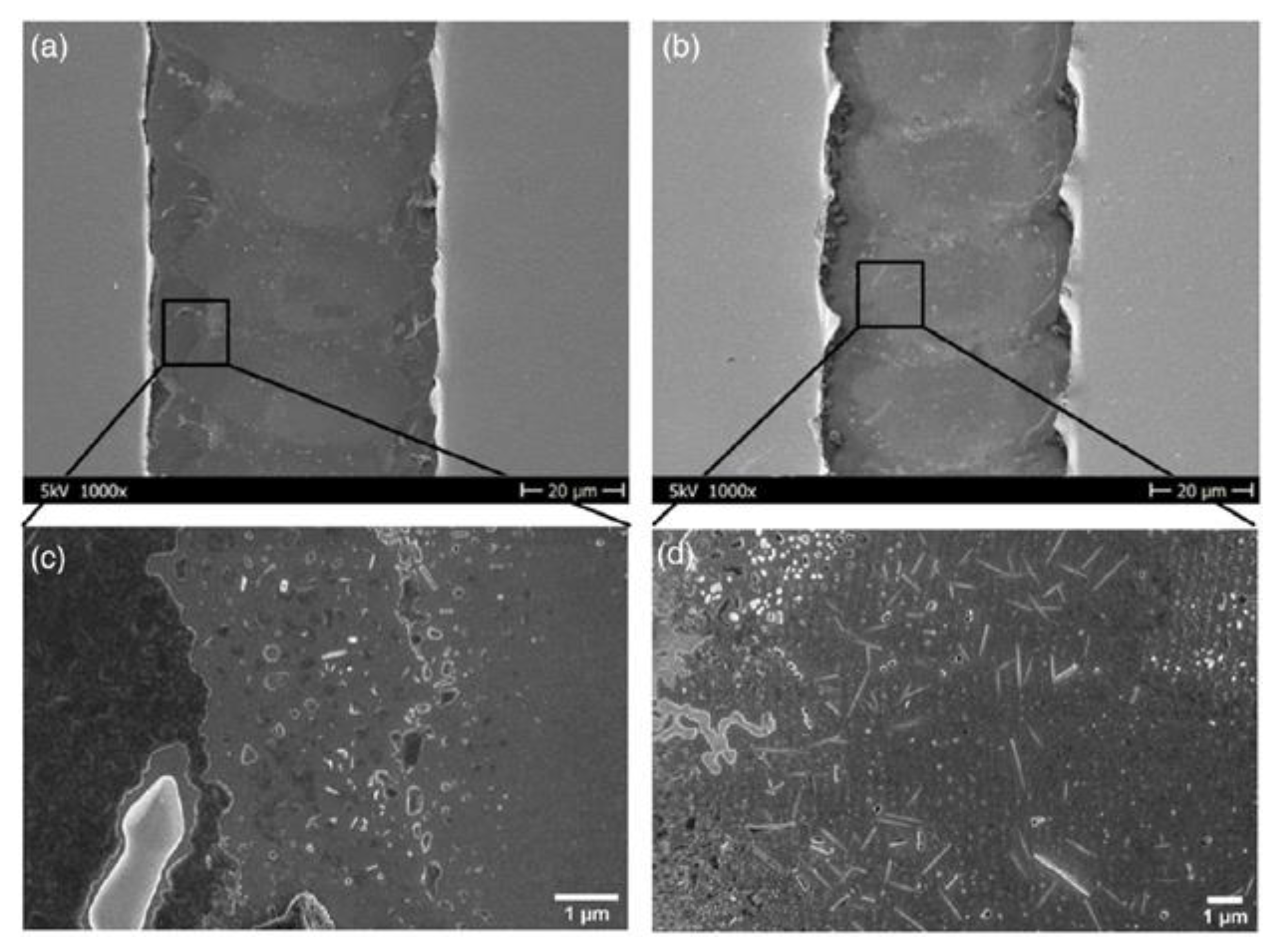
The development of thin-film photovoltaics has emerged as a promising solution to the global energy crisis within the field of solar cell technology. However, transitioning from laboratory scale to large-area solar cells requires precise and high-quality scribes to achieve the required voltage and reduce ohmic losses. Laser scribing has shown great potential in preserving efficiency by minimizing the drop in geometrical fill factor, resistive losses, and shunt formation. However, due to the laser induced photothermal effects, various defects can initiate and impact the quality of scribed grooves and weaken the module’s efficiency. In this regard, much research has been conducted to analyze the geometrical fill factor, surface integrity, and electrical performance of the laser scribes to reach higher power conversion efficiencies.
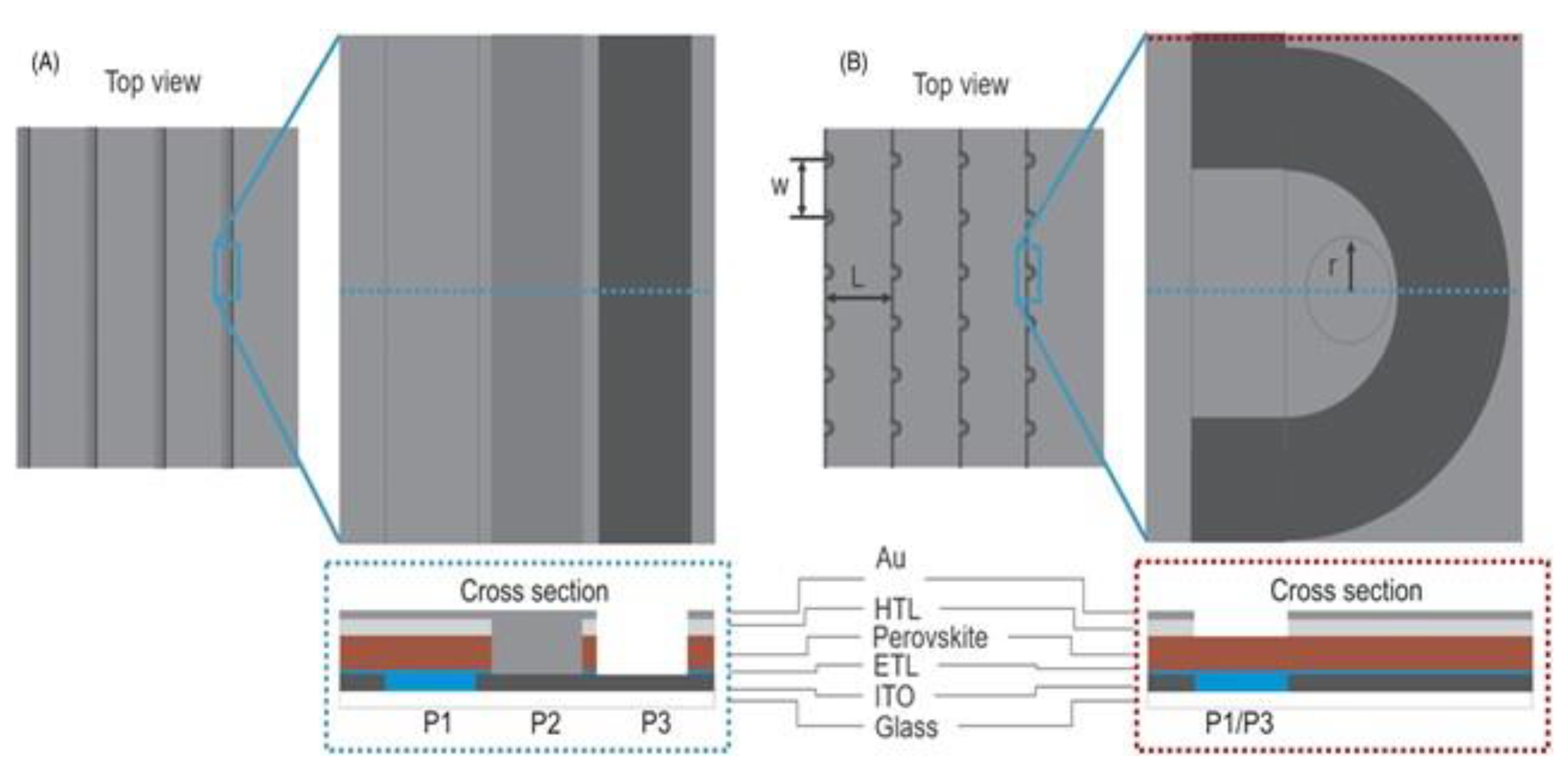
laser scribing thin film solar cell quality analysis laser scribing defects

1. Scribe Geometry

Thin film laser scribing uses different parameters that may lead to particular ablation geometries. Examination of scribe width, scribe depth, scribe cross-sectional profile, and depth selectivity are the main categories of assessing geometrical quality. Reducing scribe width and dead area from hundreds to tens of microns has been a constant goal for researchers to maximize the active area in solar cells. Furthermore, selectively removing only the desired layers with steep scribe walls has been investigated to enhance the performance of the solar cells and reduce resistance losses. To meet these demands, researchers have utilized different laser sources, parameters, and scribing techniques based on the thermal and optical properties of the material to minimize electrical losses and achieve high quality scribes.
  • Scribe depth selectivity and cross-sectional profile
Selective laser scribing is an essential feature of assessing the scribe quality, which is strongly impacted by laser parameters [1]. It has been referred to as a scribing process in which a desired depth or layer is ablated entirely without removing or damaging the underlying material [2]. Using various laser sources with different wavelengths and laser fluences, Compaan et al. [3] examined scribing depth for a wide range of metallic and semiconductor thin films. Laser wavelength was found to be an efficient factor such that selective removal of a specified layer thickness was feasible utilizing UV lasers with lower fluences. These experiments showed that the 355 nm UV light source could obtain complete and high-quality ablation with narrow groove width, due to the match between the photon energy and the material band gap energy. On the other hand, however, for the IR (infrared) laser source, poor groove profile quality has been shown because of the material pile-up on the edge of the scribes due to thermal influences [3].
Applying high laser intensities and overlapping ratios was found to directly impact crater depth, groove width, and the total ablated area, which has been verified in laser patterning of CIGS and a-Si solar cells [4][5]. However, ridge height must be addressed due to high laser fluences [3]. This phenomenon was also observed for a-Si and ITO ablation using nanosecond (ns) lasers [5][6]. It must be stated that since after P3 ablation, there is no deposition, these protrusions should not highly affect electrical performance. However, for P1 and P2, it may be more challenging to avoid efficiency reduction [7]. It was reported that this problem could be suppressed by using a large beam radius [8].
Schultz et al. [9] employed a ns laser for CIGS P2 scribing, but when a low fluence (less than 0.30 J/cm2) was applied, the resulting scribe was incomplete and of poor quality, with surface bulging observed. Additionally, higher fluences (more than 0.40 J/cm2) caused removal and damage of the molybdenum (Mo) front contact layer. Both conditions led to high series resistances; however, setting up the laser fluence in a moderate range has improved the quality of laser scribes. Shin et al. [10] investigated laser scribing of the CIS layer on Mo at different laser fluences and scanning speeds to precisely ablate the whole layer without damaging the material beneath. Accordingly, it was observed that decreasing the scanning speed will increase the ablation depth and width by melting the outer parts of the spot. It was also determined that using ultrashort pulse lasers was necessary to completely ablate the entire layer and avoid damage to the underlying films [10]. Furthermore, fs lasers can also be more efficient in reaching this goal [11]. Incomplete ablation can also impact the fill factor (FF) and current extraction in solar cell structures. This problem was actually shown to be more crucial in perovskite solar cells with a thin TiO2 scaffold interlayer between the absorber and front contact layer [12].
Scribe depth was also examined in fs single pulse irradiation of ITO on glass. The analysis by a 3D profiler demonstrated that different pulse overlaps could lead to various groove profiles. It was shown that increasing the overlap ratio from 33.2% to 98.7% could alter the scribe profile from a V shape to a U shape with steep side walls. Furthermore, to achieve desired topographical and electrical characteristics, it was illustrated that the laser scanning rate must be lower than 50 mm/s to uniformly ablate the ITO with a pulse fluence between 0.66 and 2.3 J/cm2 [13]. However, flake formation has been reported for higher overlap ratios due to a high repetition rate and reduced scanning speed, which can be a limitation to any scribe quality gain [14].
Researchers have proposed induced ablation as an alternative laser scribing technique to achieve highly selective film removal and steep wall scribes. Employing this approach for scribing CZTSe thin-film solar cells with an IR ps laser has improved removal quality, selectivity, and crater edge quality without the presence of defects [15]. Kuk et al. [16] applied induced ablation for P2 scribing of CIGS on TCO film using a 532 nm ns pulsed laser to avoid damage in the back contact layer. This research thoroughly investigated the effects of laser beam size and beam shaping. As shown in Figure 1 for P2 scribing with different beam shapes, laser fluences, and scanning speeds, the scribe width is smaller in the 24 μm beam spot, but controlling the process to prevent ITO damage is challenging. Employing a 64 μm beam spot size overcame this issue with the added benefit of increased scanning speeds. Moreover, using an elliptical shaped beam (21 μm × 84 μm) could suppress ITO damage, accompanied by narrower width, more straight grooves, and higher scanning speeds [16]. A similar induced ablation study using a ps laser confirmed the advantage of using an elliptical beam for selective film removal and high-quality scribes. Elliptical beams can also reduce the need for high beam overlapping ratios, which is an excellent asset for high-speed laser scribing and industrialization [17].
Figure 1. P2 line scribing results by (a) 24 μm diameter circular beam, (b) 64 μm diameter circular beam, and (c) 21 μm × 84 μm elliptical beam. An optical microscope and a 30° tilted SEM image are shown for each condition with laser fluence and scribing speed marked [16].
  • Laser scribing width and dead area
A simulation study on monolithic series interconnections in thin films revealed that the dead area should not be increased since it can compromise the active area and electrical efficiency [18]. It has been observed that for an active area width of 6 mm, by reducing the dead area width from 3000 to 500 μm, the total efficiency loss decreases from about 35% to 10% [18]. However, it has been demonstrated that a trade-off is also necessary for the optimization of scribe width based on the different material sheet resistance [19]. The loss factors based on the active and dead areas have been broken down into three categories, including (1) geometrical losses due to the dead zone, (2) resistive losses due to TCO, and (3) resistive losses for P2 interconnection [20][21][22]. It was revealed that reducing the P1 scribe width from the optimum point in low-resistance solar cells has dropped the efficiency [23]. Consequently, decreasing the dead zone ratio to the total area without generating resistive or shunting losses is required [24].
To reduce the scribe width, using lasers with beam quality factor M2 less than 1.3 is generally recommended [25][26]. Short wavelengths are also beneficial, as demonstrated by the results of UV laser scribing of P1, P2, and P3 for microcrystalline silicon thin film, which has led to integrated width of less than 500 µm [27]. By adjusting laser peak power, focus, and pulse width for laser scribing of silicon thin films, it was demonstrated that a 150 μm dead area width with 30, 45, and 50 μm separation could be obtained for P1, P2, and P3 ablations, respectively [28]. Furthermore, by utilizing lift-off ablation for P1 and P3 and direct ablation for P2 on CIGS solar cells, a small PV device with an initial efficiency of 18.3% was transformed into a large-area module with an efficiency reduction of less than 10%. This progress was achieved by creating a dead zone of approximately 70 μm, composed of 10, 10, and 34 μm width for P1, P2, and P3 scribes, respectively, and about 8 μm distance between adjacent scribes [29]. Heise et al. [17] used a ps laser for all three patterning processes for CIS solar thin films, with P1 being direct and induced ablation, P2 direct ablation, and P3 indirect induced ablation (removing material by lift-off from front TCO film side specifically in CIGS and CZTSe structures). Utilizing ps pulses led to narrow grooves and prevented thermal damages to the underlying layer compared to ns laser for P1 scribing, resulting in reduced dead area. Moreover, using ultrashort laser pulse irradiation, researchers reached much more constant width and cleaner scribes with minimal flake formation and delamination compared to a ns laser source [30][31]. Ultimately, using a ps laser source has shown an excellent capability to decrease the P2 CIGS scribe width to 10 μm [31].
Results of photoluminescence imaging for P2 scribing of CIGS and perovskite show that P2 scribing of perovskite leads to wider crater diameters. The wider crater is due to the fact that the significant difference in thermal conductivities between the very thin perovskite layer (650 nm) and the ITO film causes heat accumulation that expands through the interface. This problem has been a barrier to enhancing the geometrical fill factor in perovskite [32]. Moon et al. [18] performed all scribing steps of organometallic halide perovskite solar modules by laser for the first time; however, the 820 μm of dead zone width reduced the geometrical fill factor to about 16%. For laser scribing of SnO2-based perovskite with a UV ns laser, to guarantee a complete interconnection, the dead area could not be reduced to less than 600 μm [33]. Using laser for scribing P1 and mechanical scribing for P2 and P3, the dead area has been reduced to 235 μm in a cell stripe of 4.7 mm in a multijunction perovskite/CIGS thin film, which reduced the power conversion efficiency (PCE) loss to about 5% [34]. Walter et al. [12] used a UV laser for P1 glass side ablation, a green laser for glass side P2 and film side P3, and the dead area width reached about 400 μm (about 8% reduction in geometrical fill factor) for perovskite solar cells. In 2021, Yoo et al. [35] used a 532 nm ps laser that narrowed down P1, P2, and P3 scribes to 25, 105, and 80 μm scribe width, respectively; it led to a geometrical fill factor of 94.36%, efficiency of 20.4% for a mini-module, and power conversion efficiency of 17.53%. However, in 2020, Gao et al. [36] demonstrated that using ns lasers can still be a practical technique for perovskite solar cells because the absorber material has a small thermal diffusion coefficient. Moreover, the results showed a sufficient reduction of the dead area to 270 μm and a geometrical fill factor of 95.5%.
Rakocevic et al. [37] introduced a point contact interconnection design to reduce geometrical fill factor losses. Using this strategy instead of the classical line contact method was found to be promising to reduce interconnection losses to 1% and reach a geometrical fill factor of up to 99%. Figure 2 illustrates the main structural differences between point contact interconnections and classical interconnections. The design structure of this P1/P2/P3 type patterning was achieved through numerical and analytical work to approach the theoretical limit. However, the emphasis has been on demonstrating the feasibility of achieving this limit rather than developing a reliable method for reducing losses in perovskite modules [38].
Figure 2. Top view and cross section of a solar module with four cells connected in series with a magnified view of (A) classical and (B) point contact interconnections. Blue and red dotted lines indicate where the cross sections are taken. The red dotted cross section represents the part of the point contact interconnection where the P1 and P3 interconnections overlap [37].

2. Microstructure and Surface Morphology

Damages are commonly observed in laser scribing of solar thin films, including the heat-affected zone (HAZ), crack formation, debris, and film delamination. The resulting morphological and microstructural changes that occur due to the high temperatures profoundly impact the properties and performance of solar thin films. In this regard, analyzing the material resolidification after melting and the formation of residue and debris particles are pivotal factors.
The heat-affected zone is one of the dominant thermal impacts in laser scribing. HAZ refers to the region surrounding the scribe line, where the material has been affected by the heat but has not been completely removed. It has been a critical challenge for researchers in scribing solar thin films because it can lead to microcracks, structural changes, and reduced efficiency. In the case of ns laser ablation, there is a noticeable extension of the HAZ in the neighboring region, where higher melting edges and bulges can be detected [39]. It has been widely accepted that ultrashort pulse lasers, especially fs lasers, have an excellent capability of reducing the HAZ [40]. However, to minimize the HAZ, various other methods have been developed.
The results from beam shaping experiments indicate that a top-hat beam shape could yield a considerably smaller HAZ compared to a Gaussian-shaped beam in thin film laser scribing. It is shown that despite the top-hat beam causing an approximately 20% increase in scribing width, the HAZ can be reduced by more than 83%. This outcome suggests that utilizing a top-hat beam shape can be a promising technique for reducing HAZ [41].
From this point of view, induced ablation could minimize the HAZ and melted areas according to the research performed on the P1 ablation of the Mo back-contact layer [42]. Bucher et al. [43] showed that the relationship between laser fluence and the extent of the HAZ in induced P1 ablation typically follows a V-shaped plot. The HAZ is relatively high at low fluences and can increase significantly at high fluences [43][44]. However, at a mid-range fluence, stress-assisted mechanical ablation is dominant, and it can minimize the size of the HAZ [43]. Moreover, lift-off ablation can be a great fit for scribing the CIGS absorber layer due to its high sensitivity to heat-induced damage even with ultrashort lasers; rear-side ablation with pressure through the Mo layer can be beneficial in this case [45]. Furthermore, new findings regarding this process indicate that enlarged laser beams may be used to avoid damage to the ITO because of the lower absorber-ITO interfacial temperature in P2-induced ablation [16].
Thermal stress, delamination, and cracking are other common phenomena that can be generated due to the localized temperature rise and thermal expansion in thin-film laser scribing. The significance of this phenomenon stems from its negative impact on power efficiency, cell viability, and photocurrent generation [46][47]. Using a ns laser source for P3 ablation in a-Si solar cells has shown irregular scribe boundaries with peeling of the film [48]. Other studies confirm these outcomes for Mo thin-film ns laser ablation with burr formation and microcracks due to thermal effects [49][50]. Figure 3 shows damage in the underlying Mo layer caused by thermal stress that results in cracking, bulging, and delamination [9]. This challenge was observed in the P3 laser scribing at the CZTSe and Mo interface [51].
Figure 3. Cross-sectional SEM image of ps laser ablation of CIGS with crack formation, delamination, and bulging at the Mo underlying layer [9].
It has been shown that even employing ultrashort pulse lasers could not completely eliminate these defects for a-Si P2 scribing [52][53]. In this case, using infrared wavelength and high laser power increased delamination and elevated the molten rim in the surrounding edges in ps laser scribing [52]. Using glass-side laser ablation produced more delamination and microcracks due to the pressure created by the plasma expansion, which caused shockwave formation, film deformation, and brittle material cracking. New findings show that crack formation can also depend on the obtained groove profile; groove shapes with sharp vertical edges are more prone to void formation, cracking, and peeling-off in the deposited material than gradually sloped edge scribes [1].
Delamination can also be created in CdTe solar cell P2 lift-off ablation between the CdTe and CdS layers [47]. The weak adhesion between the layers can cause lateral delamination. In this case, microcracks, voids, and dislocations can be created at the tip of the delamination, as can be observed in the cross-sectional TEM images of the CdTe/CdS interface in Figure 4. This issue can be challenging since it can highly impact the long-term stability of solar thin films [54]. To overcome this barrier and minimize sheet resistance, operating at a mid-range fluence (3 J/cm2) is recommended [47]. In total, careful optimization of laser parameters plays a significant role in controlling thermal and stress-assisted damages in solar thin-film laser scribing.
Figure 4. Cross-sectional TEM images of (a) the scribe boundary and (b) magnified image at the delamination tip, showing dislocations formed at both between the two layers and grains, which may introduce further crack initiation [47].
In laser scribing processes, the material is exposed to high temperatures generated by the laser beam, leading to melting and subsequent cooling and solidification. The process of solidification after melting is referred to as resolidification, which involves the formation of a new microstructure. However, during this change, the solidification process can capture nanovoids and bubbles and trigger crack formation in the material [55][56][57]. Using pump and probe techniques, researchers could observe that melt pool formation and subsequent resolidification typically occur in a few tens of ns, and side-view shadowgraphic measurements also showed complete resolidification dynamics at 250 ns [58][59]. Employing ns laser ablation showed significant residues inside the scribe with distinct resolidified areas near the scribe line in CIGS laser ablation, but ps laser produced much cleaner trenches [32]. Three-dimensional microscopy revealed that resolidified droplets and residuals inside the trench exhibited uneven scribe profiles [60]. Furthermore, UV laser pulses have shown better capabilities in reducing droplets and debris than longer wavelength pulses [61].
Using ultrashort pulse lasers has demonstrated good capability in minimizing debris in the P1 scribing of CIGS [62]. For perovskite scribing, it has also been shown that using a ps instead of ns laser could decrease needle-like PbI2 residues, the typical byproduct of perovskite’s thermal decomposition in the groove [30][63]. An optimum laser fluence was found to be more desirable since scribing in low fluence could leave a poorly scribed trench with melting and residues [64][65], and in higher fluence, solidified rims, bubbles, and splashes may remain. This phenomenon is shown in Figure 5 in both ns and ps laser scribing [64]. Higher pulse repetition rates could generate more voids and residues at the trench [66]. Furthermore, a top-hat beam could be more promising in minimizing residues, recast, and debris in laser scribing than a Gaussian beam [36][67].
Figure 5. SEM images of (a) ns and (b) ps laser patterned P2 scribe-lines at different fluences (the magnification of all images: 1000×) [64].
The use of induced ablation can significantly reduce the residual formation and redeposited material due to the prevention of plasma shielding and the protection of the film/carrier interface from debris. However, particular challenges associated with this procedure must be addressed [25][68][69]. Similar to direct ablation, there is an optimum value for laser fluence. Ablating film at lower and higher fluence can cause material melting and resolidification with the formation of nanobubbles and rims; this phenomenon has been captured in AZO, SnO2, and CdTe/CdS lift-off ablation [39][47][70]. In addition, increasing the overlap ratio to an optimum value has been recommended regarding residue [70].
Results obtained in [71] revealed that droplets and debris in the P2-induced ablation of perovskite could create a broad line of residues in the center of the groove. For minimizing residue and recast layers, combining the lift-off process with a fs laser can be a practical approach to attaining a debris and damage-free surface in laser scribing of an a-Si solar cell [72]. Alternatively, using an elliptical beam in combination with the lift-off process has attained clean scribes with minimum residues [16].

3. Chemical Composition and Reaction

Laser scribing of solar thin films may induce chemical modifications to surface and subsurface materials, necessitating chemical analysis as an essential investigative technique to discern and understand their effects on cell performance. Diffusion and phase transformation at the interface are common phenomena that can occur during the process due to the high temperature and thermal gradient induced by the laser beam. Additionally, the high temperature generated by the laser can also cause oxidation in both the metallic elements of the absorber layer and the metallic conductive films.
For complex multicomponent materials such as CIGS and CZTSe, the laser heat effect can cause the formation of secondary phases [51][73]. One of the most important front contact layer damages in these solar thin films is linked to considerable intermetallic diffusion and phase transformation occurring at high temperatures of the absorber−TCO interface or during the molten stage in P2 ablation. The key objective in CIGS P2 ablation is to limit the spread of unwanted intermetallic CIGS constituents towards the upper surface of the bottom contact film during the P2 scribing procedure, as this is necessary for preserving low contact resistance [16].
It has been observed that ns laser scribing of the CIS absorber layer can cause interdiffusion between resolidified CIS and Mo. In contrast, ps laser scribing could minimize interdiffusion and secondary phase formation [74][75]. Furthermore, laser scribing can cause partial evaporation. In this regard, creating a groove for P2 CIGS through laser scribing, which results in an abundance of resolidified conductive materials such as copper and a reduced presence of non-conductive elements residue, such as selenium, is not undesirable, because it can increase conductivity in the P2 trench [9][76]. A study investigated the effect of laser fluence (0.28–0.73 J/cm2) on the phase transformation during P2 scribing of CIGS. It was reported that scribing in an intermediate fluence caused metal elements enrichment and reduced Se element on the bottom contact layer and scribing walls, which could reduce resistance in the scribing groove. This study found the optimum fluence at 0.36 J/cm2, and increasing or decreasing fluence increased Se and reduced metallic elements in the residues [9].
For P3 processing of CIGS solar cells with a ps laser, it has been shown that scribing both the back contact layer and absorber film can generate conductive phases, such as Mo, at the scribing edges that can connect back and front contact instead of isolation. Scribing only the upper conductive layer seems more efficient due to the lack of Mo exposure on the walls [77]. Better performance for removing only the back contact layer in the P3 scribe has also been confirmed for CZTSe solar cells [15]. Figure 6 shows the energy-dispersive X-ray spectroscopy (EDS) analysis of P3 scribing of CIGS and AZO with a cumulative thickness of about 1.95 μm. It can be observed that in a partial removal (1.3 μm), due to high intensity in the center of the groove, Mo diffusion inside the scribe can be detected (Figure 6a). It also can be seen that in the complete ablation of 1.95 μm, indium is almost removed entirely and Mo diffusion increases effectively with starting diffusion of Si element of the glass substrate (Figure 6b) [78].
Figure 6. SEM image (left), and EDS measurement (right) of the slot; (a) laser fluence: 4.5 J/cm2, overlap ratio: 81%, ablation depth: 1.3 μm, (b) laser fluence: 4.5 J/cm2; overlap ratio: 87%; ablation depth: 1.95 μm [78].
The diffusion of material during laser scribing can be affected by the composition of the absorber material, which can alter the bandgap and absorption properties of the material. Figure 7 illustrates the effects of Ga concentration (xGa) in the CIGS layer scribing at different laser fluences [65]. It is shown that xGa > 0.2 is more effective in reducing residues and secondary phase creation. Scanning electron microscopy (SEM) images illustrate that scribing using high laser fluence may lead to unfavorable outcomes and suboptimal scribes, accompanied by the presence of secondary phases [65].
Figure 7. SEM images of the craters produced on the CIGS samples with different Ga concentrations at varying laser fluence [65].
Diffusion can also occur in perovskite solar cells, which was proved in the Raman spectra in a study of laser scribing using a ns Gaussian beam. Due to the Gaussian beam intensity profile, ITO residue was detected at points near the P2 scribe center, and using pulse energy of about 2 μJ was able to mitigate the issue [36]. For P3 scribing, gold flakes could be detected, creating a short circuit between the two adjacent sub-modules. Using higher fluence also showed a suitable ability to minimize this problem [79].
It has been discovered that ps laser scribing can initiate perovskite compositional change up to 4 μm away from the P3 scribe in the active area, and the changes in the composition of the perovskite layer adjacent to the scribe line were due to the existence of PbI2 grains [80]. Compositional analysis in a ns laser scribing study showed a large amount of needle-shaped PbI2 produced in the P3 scribe and a thin Br-rich layer formation at the perovskite/HTL interface extended up to 12 μm from the edge of the P3 line [30]. Figure 8 displays SEM images for ns and ps P3 perovskite scribing. The needle-shaped grains are identified as PbI2. It can be inferred that ns pulses can readily generate both PbI2 residues and a Br-rich layer, which passivate electronic defect states located at the edges of the scribe line and impede the movement of charge carriers in the surrounding regions [30]. However, it should be indicated that PbI2-containing debris in P2 scribing is not desirable since it can lead to comparatively weak conductivity and impede low-resistance contact [71].
Figure 8. SEM images of the laser-scribed lines patterned by (a) ps and (b) ns laser pulses with fluences of 2.31 and 1.36 J cm−2, respectively. The black squares schematically show the positions of the high-magnification images of the (c) ps and (d) ns laser scribe lines [30].
Furthermore, in the case of laser scribing of metallic layers in reactive environments, such as air, precautions must be taken to avoid inter-pulse chemical reactions that can result in changes to the surface chemistry, such as oxidation, that can leave oxide deposits inside the groove and thus increase ohmic losses [40][68][81]. These reactions can also occur in solar cells with a buffer layer of CdS. The oxidation of sulfur can occur rapidly, resulting in its conversion into a gaseous phase. It can become stuck within the CdS matrix, where it may form bubbles upon secondary phase formation, which can ultimately create microcracks and weaken the electrical properties of the solar cell [47].
A double scribe method with UV ns laser has been proposed to minimize potential oxidation in laser scribing and reduce contact resistance in the P2 scribe. It has been demonstrated that the first scribe leaves a large amount of absorber oxide deposits inside the groove, and the second scribe removes most of them and leaves a minimum SiO2 phase in the trench [82]. In this context, laser scribing in a vacuum with a pressure of 1.5 × 10⁻⁵ mbar as an alternative way has shown much cleaner scribes with fewer residues and lower resistance [21][83]. In order to avoid the formation of undesired oxides and degradation of perovskite material due to oxidation, laser patterning has also been performed inside a glovebox filled with nitrogen. As a result, the scribes were clean and free from any residual material [84].

4. Electrical Characteristics

Preserving thin film solar PV efficiency from laboratory to industrial scale needs accurate control and selection of laser parameters and scribing techniques. Laser scribing could adversely impact the efficiency of solar cells by increasing the series resistance, decreasing their shunt resistance, and ultimately reducing the fill factor. These effects result from nonselective ablation and thermomechanical damage to underlying layers of the solar cell and the creation of new electrical paths through the cell, leading to current leakage and reduced performance [85]. Therefore, finding suitable laser parameters and techniques is crucial to minimize the efficiency loss due to laser scribing.
There is a direct correlation between increasing efficiency and decreasing dead area; however, ohmic losses and shunt formation should be considered. It has been reported that reducing dead area from 430 to 230 μm enhanced cell efficiency from 13.6% to 15.2% [32]. On the other hand, it has been shown that decreasing the P1 scribe width from 100 to 10 μm may not change the electrical properties of the line and cell [61]. However, module electrical properties may depend more on P2 and P3 scribing quality than on P1 scribing. In this regard, while Kubis et al. [7] declared that the interconnection width of 17 μm may be enough to ensure current transport without loss in the P2 scribe, the experimental results in another research showed that modules with a narrow P2 scribe of about 40 μm and a P3 scribe as narrow as 30 μm in perovskite solar cells could result in drop off in current and decrease in voltage [38]. Table 1 shows the combinations of P2 scribe widths (a = 40, b = 160, and c = 320 μm) with P3 scribe widths (α = 30, β = 90, and γ = 150 μm) and their J–V (current–voltage) characteristics. The highest performing result occurs in “bβ” with a geometrical fill factor of 91% and power conversion efficiency (PCE) of 18.71%. It can be inferred that increasing the geometrical fill factor (GFF) from 91% to higher values decreases efficiency due to ohmic losses. Therefore, studying groove quality with consideration of material characteristics is necessary to correlate inactive area reduction and solar cell efficiency.
Table 1. J–V parameters of each module type fabricated. Voc (open-circuit voltage) is calculated as the sum of three connected cells in series, Isc is the short-circuit current, and Jsc is the short-circuit current density. Adapted with permission from [38].
For P2 and P3 scribing, it has been demonstrated that direct laser scribing below the damage threshold can create a shunt between layers, which can damage the p-n junction [85]. This damage can be intensified using lasers with low beam quality (M2). It was shown that using Nd:YAG lasers with M2 > 1.6 could generate poor-quality scribes with residuals such as Sn and In in CdTe solar cells. These elements could diffuse and reach the junction area to create defects and increase electrical shunts, leading to a reduction in the parallel resistance (Rsh) of the device [25].
To reach high efficiency, high groove resistance is needed for P1 and P3 and low resistance for P2. Increasing laser fluence was found to promote complete ablation and elevate line resistance in P1 and P3 scribes [39][86]. However, high laser fluence may result in damage to the underlying layer due to overheating. It may also leave a resolidified layer, which could contribute to the formation of a substantial shunt and the undesirable reduction in parallel resistance [87]. Therefore, careful selection of optimum and suitable conditions for laser fluence in solar thin film scribing is needed. Figure 9 demonstrates how this could be done by studying the relationship between laser fluence and power conversion efficiency in the P3 scribing of perovskite solar cells [30].
Figure 9. Box-plot of the mini-module PCE as a function of the applied laser fluence for P3 patterning by (a) ps and (b) ns laser pulses [30].
To decrease defect and shunt formation in the scribes, using top hat beams and ultrashort pulse lasers can be more efficient [88]. Due to selective ablation and lower temperatures generated in top-hat beam laser scribing compared to Gaussian beam, diffusion, secondary phase formation, and damage to underlying layers can be minimized to achieve better electrical characteristics [41][67]. The application of ultrashort laser pulses has the potential to reduce the formation of defects at the scribing edges of a profile, thereby circumventing the negative impact of such defects on the electrical characterizations of the material [32]. It has been observed that ablating with a ns laser leads to formation of a liquid layer and residues of non-ablated material, particularly concentrated in the bordering zone of the ablation channel in P3 patterning. This zone contains metal residues in contact with the ZnO layer, causing a shunt between the Mo and ZnO layers. Using ns lasers may noticeably decrease the efficiency of the solar thin films, and ps and fs lasers have demonstrated much less efficiency drop in thin film solar cells [74][89].
Furthermore, it must be mentioned that laser-type selection depends on the type of scribing and the film material to be removed. In P2 scribing of perovskite, a ns laser is not desirable since it can generate non-conductive materials such as residues and debris. However, it can be beneficial in P3 scribing, where high isolation and resistance are demanded [30][71]. This selection strategy is also effective in multi-compositional materials such as CIGS and CZTSe. Additionally, the researchers have observed that the implementation of the lift-off process in conjunction with ultrashort pulsed laser ablation did not result in any noticeable degradation of the electrical properties of the thin film solar cells, which is attributed to the effective mitigation of secondary phase formation and structural disorders within the trench [15]. However, indirectly induced ablation of CZTSe using ps and fs lasers has shown contradictory results. It was found that scribing CZTSe with a 300 fs laser caused nonlinear absorption effects leading to a higher P3 line conductivity and reduced efficiency compared to using a 60 ps laser [51]. Along with laser pulse width and scribing method, choosing a suitable wavelength based on the optical properties of the material is necessary. For example, ps laser scribing of CIGS caused less efficiency drop with infrared wavelength than green wavelength due to less melt formation and heat effects at the scribing edge. However, for P3 scribing of CIGS, green lasers showed better performance [74][90].
For P3 patterning of CIGS, as shown in Figure 10, type 1 scribing, which removes both the absorber and the front contact layer at a 200–1000 kHz repetition rate, has higher scribe conductance than type 2 scribing of the front contact layer only at a 100 kHz repetition rate [90][91]. The phenomenon can be attributed to a significant increase in the amount of the resolidified conductive layer within the type 1 groove [92]. Eventually, it has resulted in a lower fill factor value and efficiency for type 1 scribing [93].
Figure 10. (a) Laser scribe conductivity based on laser repetition rate for P3 type 1 and type 2, (b) module electrical performance for type 1 and 2 [90].
Two other methods have also been used for laser scribing of solar thin films to enhance conversion efficiency. The first technique is a combination of thermal annealing with femtosecond laser scribing. It has been shown that thermal annealing in a moderate temperature range between 50 and 200 °C after laser scribing can boost power conversion efficiency, as verified by J–V curve measurements before and after annealing. The enhancement in the efficiency of the solar thin film is attributed to the removal of defect states induced by the laser, which are concentrated in high densities near the p-n junction and the edges of the scribe [94]. A two-pass laser scribing is the second method for increasing solar thin film efficiency. The idea is to use the second pass to remove the high amount of debris left inside the trench from the first pass. The efficacy of this approach was demonstrated in a study of ns laser scribing of perovskite solar cells by comparing the scribing quality before and after the second pass. It can be inferred that by employing this technique, solar cell efficiency can be positively impacted with minimum resistive losses [19].

References

  1. Li, J.; Niu, J.; Wu, X.; Kong, Y.; Gao, J.; Zhu, J.; Li, Q.; Huang, L.; Wang, S.; Chi, Z.; et al. Effects of Laser-Scribed Mo Groove Shape on Highly Efficient Zn(O,S)-Based Cu(In,Ga)Se2 Solar Modules. Sol. RRL 2020, 4, 1900510.
  2. Stegemann, B.; Schultz, C. Laser Patterning of Thin Films. In Digital Encyclopedia of Applied Physics; Wiley-VCH Verlag GmbH & Co. KGaA: Weinheim, Germany, 2019; pp. 1–30.
  3. Compaan, A.D.; Matulionis, I.; Nakade, S. Laser Scribing of Polycrystalline Thin Films. Opt. Lasers Eng. 2000, 34, 15–45.
  4. Bian, Q.; Yu, X.; Zhao, B.; Chang, Z.; Lei, S. Femtosecond Laser Patterning of Mo Thin Film on Flexible Substrate for Cigs Solar Cells. In Proceedings of the 30th International Congress on Applications of Lasers and Electro-Optics, ICALEO 2011, Orlando, FL, USA, 23–27 October 2011; pp. 869–874.
  5. Lauzurica, S.; Molpeceres, C. Assessment of Laser Direct-Scribing of a-Si:H Solar Cells with UV Nanosecond and Picosecond Sources. Phys. Procedia 2010, 5, 277–284.
  6. Molpeceres, C.; Lauzurica, S.; Ocãa, J.L.; Gandía, J.J.; Urbina, L.; Cárabe, J. Microprocessing of ITO and A-Si Thin Films Using Ns Laser Sources. J. Micromechanics Microengineering 2005, 15, 1271–1278.
  7. Kubis, P.; Li, N.; Stubhan, T.; Machui, F.; Matt, G.J.; Voigt, M.M.; Brabec, C.J. Patterning of Organic Photovoltaic Modules by Ultrafast Laser. Prog. Photovolt. Res. Appl. 2015, 23, 238–246.
  8. Ben-Yakar, A.; Harkin, A.; Ashmore, J.; Byer, R.L.; Stone, H.A. Thermal and Fluid Processes of a Thin Melt Zone during Femtosecond Laser Ablation of Glass: The Formation of Rims by Single Laser Pulses. J. Phys. D Appl. Phys. 2007, 40, 1447–1459.
  9. Schultz, C.; Schuele, M.; Stelmaszczyk, K.; Weizman, M.; Gref, O.; Friedrich, F.; Wolf, C.; Papathanasiou, N.; Kaufmann, C.A.; Rau, B.; et al. Laser-Induced Local Phase Transformation of CIGSe for Monolithic Serial Interconnection: Analysis of the Material Properties. Sol. Energy Mater. Sol. Cells 2016, 157, 636–643.
  10. Shin, Y.C.; Cheng, G.J.; Hu, W.; Zhang, M.Y.; Lee, S. High Precision Scribing of Thin Film Solar Cells by a Picosecond Laser. In Proceedings of NSF Engineering Research and Innovation Conference, Atlanta, GA, USA, 4–7 January 2011.
  11. Bian, Q.; Yu, X.; Zhao, B.; Chang, Z.; Lei, S. Femtosecond Laser Ablation of Indium Tin-Oxide Narrow Grooves for Thin Film Solar Cells. Opt. Laser Technol. 2013, 45, 395–401.
  12. Walter, A.; Moon, S.J.; Kamino, B.A.; Lofgren, L.; Sacchetto, D.; Matteocci, F.; Taheri, B.; Bailat, J.; di Carlo, A.; Ballif, C.; et al. Closing the Cell-to-Module Efficiency Gap: A Fully Laser Scribed Perovskite Minimodule with 16% Steady-State Aperture Area Efficiency. IEEE J. Photovolt. 2018, 8, 151–155.
  13. Bian, Q.; Shen, X.; Chen, S.; Chang, Z.; Lei, S. Femtosecond Laser Ablation of Indium Tin Oxide (ITO) Glass for Fabrication of Thin Film Solar Cells; Laser Institute of America: Orlando, FL, USA, 2010.
  14. Haas, S.; Gordijn, A.; Stiebig, H. High Speed Laser Processing for Monolithical Series Connection of Silicon Thin-Film Modules. Prog. Photovolt. Res. Appl. 2008, 16, 195–203.
  15. Gecys, P.; Markauskas, E.; Gedvilas, M.; Raciukaitis, G.; Repins, I.; Beall, C. Ultrashort Pulsed Laser Induced Material Lift-off Processing of CZTSe Thin-Film Solar Cells. Sol. Energy 2014, 102, 82–90.
  16. Kuk, S.; Wang, Z.; Jia, Z.; Zhang, T.; Park, J.K.; Kim, W.M.; Wang, L.; Jeong, J.H.; Hwang, D.J. Effect of Nanosecond Laser Beam Shaping on Cu(In,Ga)Se2 Thin Film Solar Cell Scribing. ACS Appl. Energy Mater. 2019, 2, 5057–5065.
  17. Heise, G.; Börner, A.; Dickmann, M.; Englmaier, M.; Heiss, A.; Kemnitzer, M.; Konrad, J.; Moser, R.; Palm, J.; Vogt, H.; et al. Demonstration of the Monolithic Interconnection on CIS Solar Cells by Picosecond Laser Structuring on 30 by 30 Cm2 Modules. Prog. Photovolt. Res. Appl. 2015, 23, 1291–1304.
  18. Moon, S.J.; Yum, J.H.; Lofgren, L.; Walter, A.; Sansonnens, L.; Benkhaira, M.; Nicolay, S.; Bailat, J.; Ballif, C. Laser-Scribing Patterning for the Production of Organometallic Halide Perovskite Solar Modules. IEEE J. Photovolt. 2015, 5, 1087–1092.
  19. Turan, B.; Huuskonen, A.; Kühn, I.; Kirchartz, T.; Haas, S. Cost-Effective Absorber Patterning of Perovskite Solar Cells by Nanosecond Laser Processing. Sol. RRL 2017, 1, 1700003.
  20. Di Giacomo, F.; Castriotta, L.A.; Kosasih, F.U.; Di Girolamo, D.; Ducati, C.; Di Carlo, A. Upscaling Inverted Perovskite Solar Cells: Optimization of Laser Scribing for Highly Efficient Mini-Modules. Micromachines 2020, 11, 1127.
  21. Turan, B.T.; Haas, S. Scribe Width Optimization of Absorber Laser Ablation for Thin-Film Silicon Solar Modules. J. Laser Micro Nanoeng. 2013, 8, 230–233.
  22. Palma, A.L.; Matteocci, F.; Agresti, A.; Pescetelli, S.; Calabrò, E.; Vesce, L.; Christiansen, S.; Schmidt, M.; di Carlo, A. Laser-Patterning Engineering for Perovskite Solar Modules with 95% Aperture Ratio. IEEE J. Photovolt. 2017, 7, 1674–1680.
  23. Brecl, K.; Topič, M.; Smole, F. A Detailed Study of Monolithic Contacts and Electrical Losses in a Large-Area Thin-Film Module. Prog. Photovolt. Res. Appl. 2005, 13, 297–310.
  24. Kothandaraman, R.K.; Jiang, Y.; Feurer, T.; Tiwari, A.N.; Fu, F. Near-Infrared-Transparent Perovskite Solar Cells and Perovskite-Based Tandem Photovoltaics. Small Methods 2020, 4, 2000395.
  25. Bosio, A.; Sozzi, M.; Menossi, D.; Selleri, S.; Cucinotta, A.; Romeo, N. Polycrystalline CdTe Thin Film Mini-Modules Monolithically Integrated by Fiber Laser. Thin Solid Film. 2014, 562, 638–647.
  26. Endert, H.; Niederhofer, J. Two Concepts Changing Laser Scribing in Photovoltaics. Laser Tech. J. 2011, 8, 25–28.
  27. Kuo, C.F.J.; Tu, H.M.; Liang, S.W.; Tsai, W.L. Optimization of Microcrystalline Silicon Thin Film Solar Cell Isolation Processing Parameters Using Ultraviolet Laser. Opt. Laser Technol. 2010, 42, 945–955.
  28. Tsai, C.Y.; Tsai, C.Y. Development of Amorphous/Microcrystalline Silicon Tandem Thin-Film Solar Modules with Low Output Voltage, High Energy Yield, Low Light-Induced Degradation, and High Damp-Heat Reliability. J. Nanomater. 2014, 2014, 861741.
  29. Nishiwaki, S.; Burn, A.; Buecheler, S.; Muralt, M.; Pilz, S.; Romano, V.; Witte, R.; Krainer, L.; Spühler, G.J.; Tiwari, A.N. A Monolithically Integrated High-Efficiency Cu(In,Ga)Se2 Mini-Module Structured Solely by Laser. Prog. Photovolt. Res. Appl. 2015, 23, 1908–1915.
  30. Fenske, M.; Schultz, C.; Dagar, J.; Kosasih, F.U.; Zeiser, A.; Junghans, C.; Bartelt, A.; Ducati, C.; Schlatmann, R.; Unger, E.; et al. Improved Electrical Performance of Perovskite Photovoltaic Mini-Modules through Controlled PbI2 Formation Using Nanosecond Laser Pulses for P3 Patterning. Energy Technol. 2021, 9, 2000969.
  31. Schultz, C.; Weizman, M.; Schüle, M.; Juzumas, V.; Stelmaszczyk, K.; Wolf, C.; Papathanasiou, N.; Rau, B.; Schlatmann, R.; Quaschning, V.; et al. Laser Patterning of CIGSe Solar Cells Using Nano-and Picosecond Pulses-Possibilities and Challenges. In Proceedings of the 28th European Photovoltaic Solar Energy Conference, Paris, France, 30 September–4 October 2013.
  32. Schultz, C.; Fenske, M.; Dagar, J.; Farias Basulto, G.A.; Zeiser, A.; Bartelt, A.; Junghans, C.; Schlatmann, R.; Unger, E.; Stegemann, B. Laser-Based Series Interconnection of Chalcopyrite Und Perovskite Solar Cells: Analysis of Material Modifications and Implications for Achieving Small Dead Area Widths. Mater. Today Proc. 2021, 53, 299–306.
  33. Taheri, B.; de Rossi, F.; Lucarelli, G.; Castriotta, L.A.; di Carlo, A.; Brown, T.M.; Brunetti, F. Laser-Scribing Optimization for Sprayed SnO2-Based Perovskite Solar Modules on Flexible Plastic Substrates. ACS Appl. Energy Mater. 2021, 4, 4507–4518.
  34. Paetzold, U.W.; Jaysankar, M.; Gehlhaar, R.; Ahlswede, E.; Paetel, S.; Qiu, W.; Bastos, J.; Rakocevic, L.; Richards, B.S.; Aernouts, T.; et al. Scalable Perovskite/CIGS Thin-Film Solar Module with Power Conversion Efficiency of 17.8%. J. Mater. Chem. A 2017, 5, 9897–9906.
  35. Yoo, J.W.; Jang, J.; Kim, U.; Lee, Y.; Ji, S.G.; Noh, E.; Hong, S.; Choi, M.; Seok, S. il Efficient Perovskite Solar Mini-Modules Fabricated via Bar-Coating Using 2-Methoxyethanol-Based Formamidinium Lead Tri-Iodide Precursor Solution. Joule 2021, 5, 2420–2436.
  36. Gao, Y.; Liu, C.; Xie, Y.; Guo, R.; Zhong, X.; Ju, H.; Qin, L.; Jia, P.; Wu, S.; Schropp, R.E.I.; et al. Can Nanosecond Laser Achieve High-Performance Perovskite Solar Modules with Aperture Area Efficiency Over 21%? Adv. Energy Mater. 2022, 12, 2202287.
  37. Rakocevic, L.; Schöpe, G.; Turan, B.; Genoe, J.; Aernouts, T.; Haas, S.; Gehlhaar, R.; Poortmans, J. Perovskite Modules with 99% Geometrical Fill Factor Using Point Contact Interconnections Design. Prog. Photovolt. Res. Appl. 2020, 28, 1120–1127.
  38. Castriotta, L.A.; Zendehdel, M.; Yaghoobi Nia, N.; Leonardi, E.; Löffler, M.; Paci, B.; Generosi, A.; Rellinghaus, B.; Di Carlo, A. Reducing Losses in Perovskite Large Area Solar Technology: Laser Design Optimization for Highly Efficient Modules and Minipanels. Adv. Energy Mater. 2022, 12, 2103420.
  39. Krause, S.; Miclea, P.T.; Steudel, F.; Schweizer, S.; Seifert, G. Few Micrometers Wide, Perfectly Isolating Scribes in Transparent Conductive Oxide Layers Prepared by Femtosecond Laser Processing. J. Renew. Sustain. Energy 2014, 6, 011402.
  40. Bonse, J.; Krüger, J. Probing the Heat Affected Zone by Chemical Modifications in Femtosecond Pulse Laser Ablation of Titanium Nitride Films in Air. J. Appl. Phys. 2010, 107, 054902.
  41. Brandal, G.; Ardelean, J.; O’Gara, S.; Chen, H.; Yao, Y.L. Comparative Study of Laser Scribing of SnO2:F Thin Films Using Gaussian and Top-Hat Beams; International Congress on Applications of Lasers & Electro-Optics; Laser Institute of America: Orlando, FL, USA, 2018; pp. 130–139.
  42. Kim, T.W.; Lee, J.Y.; Kim, D.H.; Pahk, H.J. Ultra-Short Laser Patterning of Thin-Film CIGS Solar Cells through Glass Substrate. Int. J. Precis. Eng. Manuf. 2013, 14, 1287–1292.
  43. Bucher, T.; Brandal, G.; Chen, H.; Yao, Y.L. Quantifying the Heat Affected Zone in Laser Scribing of Thin Film Solar Cells. Manuf. Lett. 2017, 13, 11–14.
  44. Schneller, E.; Dhere, N.G.; Shimada, J.; Kar, A. Study of the Laser Scribing of Molybdenum Thin Films Fabricated Using Different Deposition Techniques. In Proceedings of the Laser Material Processing for Solar Energy Devices II, San Diego, CA, USA, 16 September 2013; Volume 8826, p. 88260C.
  45. Witte, R.; Frei, B.; Schneeberger, S.; Bücheler, S.; Nishiwaki, S.; Burn, A.; Muralt, M.; Romano, V.; Krainer, L. Investigation of a Reliable All-Laser Scribing Process in Thin Film Cu(In,Ga)(S,Se) 2 Manufacturing. In Proceedings of the Laser Applications in Microelectronic and Optoelectronic Manufacturing (LAMOM) XVIII, San Francisco, CA, USA, 13 March 2013; Volume 8607, p. 86071B.
  46. Kajari-Schröder, S.; Bjorneklett, B.; Köntges, M.; Kunze, I.; Kajari-Schröder, S.; Breitenmoser, X.; Bjørneklett, B. Quantifying the risk of power loss in PV modules due to micro cracks. In Proceedings of the 25th European Photovoltaic Solar Energy Conference, Valencia, Spain, 6–10 September 2010.
  47. Wang, H.; Yao, Y.L.; Chen, H. Removal Mechanism and Defect Characterization for Glass-Side Laser Scribing of CdTe/CdS Multilayer in Solar Cells. J. Manuf. Sci. Eng. Trans. ASME 2015, 137, 061006.
  48. Lauzurica, S.; García-Ballesteros, J.J.; Colina, M.; Sánchez-Aniorte, I.; Molpeceres, C. Selective Ablation with UV Lasers of A-Si:H Thin Film Solar Cells in Direct Scribing Configuration. Appl. Surf. Sci. 2011, 257, 5230–5236.
  49. Tamaoki, S.; Kaneuchi, Y.; Kakui, M.; Baird, B.; Paudel, N.R.; Wieland, K. Development of Wide Operational Range Fiber Laser for Processing Thin Film Photovoltaic Panels. In Proceedings of the International Congress on Applications of Lasers & Electro-Optics, Anaheim, CA, USA, 26–30 September 2010; pp. 1220–1225.
  50. Domke, M.; Rapp, S.; Schmidt, M.; Huber, H.P. Ultrafast pump-probe microscopy with high temporal dynamic range. Opt. Express 2012, 20, 10330–10338.
  51. Markauskas, E.; Gečys, P.; Repins, I.; Beall, C.; Račiukaitis, G. Laser Lift-off Scribing of the CZTSe Thin-Film Solar Cells at Different Pulse Durations. Sol. Energy 2017, 150, 246–254.
  52. Kim, T.-W.; Pahk, H.-J.; Park, H.K.; Hwang, D.J.; Grigoropoulos, C.P. Comparison of Multilayer Laser Scribing of Thin Film Solar Cells with Femto, Pico, and Nanosecond Pulse Durations. In Proceedings of the Thin Film Solar Technology, San Diego, CA, USA, 20 August 2009; Volume 7409, p. 74090A.
  53. Gečys, P.; Račiukaitis, G. Scribing of A-Si Thin-Film Solar Cells with Picosecond Laser. Eur. Phys. J. Appl. Phys. 2010, 51, 33209.
  54. Hongliang Wang, A. Laser Surface Texturing, Crystallization and Scribing of Thin Films in Solar Cell; Columbia University: New York, NY, USA, 2013.
  55. Wu, C.; Zhigilei, L.V. Microscopic Mechanisms of Laser Spallation and Ablation of Metal Targets from Large-Scale Molecular Dynamics Simulations. Appl. Phys. A 2014, 114, 11–32.
  56. Xia, Y.; Jing, X.; Zhang, D.; Wang, F.; Jaffery, S.H.I.; Li, H. A Comparative Study of Direct Laser Ablation and Laser-Induced Plasma-Assisted Ablation on Glass Surface. Infrared Phys. Technol. 2021, 115, 103737.
  57. Sun, M.; Eppelt, U.; Hartmann, C.; Schulz, W.; Zhu, J.; Lin, Z. Damage Morphology and Mechanism in Ablation Cutting of Thin Glass Sheets with Picosecond Pulsed Lasers. Opt. Laser Technol. 2016, 80, 227–236.
  58. Bonse, J.; Bachelier, G.; Siegel, J.; Solis, J. Time- and Space-Resolved Dynamics of Melting, Ablation, and Solidification Phenomena Induced by Femtosecond Laser Pulses in Germanium. Phys. Rev. B 2006, 74, 134106.
  59. Unger, C.; Koch, J.; Overmeyer, L.; Chichkov, B.N. Time-Resolved Studies of Femtosecond-Laser Induced Melt Dynamics. Opt. Express 2012, 20, 24864–24872.
  60. Pem, F.J.; Mansfield, L.; Glynn, S.; To, B.; Dehart, C.; Nikumb, S.; Dinkel, C.; Rekow, M.; Murison, R.; Panarello, T.; et al. All-Laser Scribing for Thin-Film CuInGaSe2 Solar Cells. In Proceedings of the 2010 35th IEEE Photovoltaic Specialists Conference, Honolulu, HI, USA, 20–25 June 2010; pp. 3479–3484.
  61. García-Ballesteros, J.J.; Lauzurica, S.; Molpeceres, C.; Torres, I.; Canteli, D.; Gandía, J.J. Electrical Losses Induced by Laser Scribing during Monolithic Interconnection of Devices Based on A-Si:H. Phys. Procedia 2010, 5, 293–300.
  62. Chang, T.L.; Chen, C.Y.; Wang, C.P. Precise Ultrafast Laser Micromachining in Thin-Film CIGS Photovoltaic Modules. Microelectron. Eng. 2013, 110, 381–385.
  63. Juarez-Perez, E.J.; Ono, L.K.; Maeda, M.; Jiang, Y.; Hawash, Z.; Qi, Y. Photodecomposition and Thermal Decomposition in Methylammonium Halide Lead Perovskites and Inferred Design Principles to Increase Photovoltaic Device Stability. J. Mater. Chem. A 2018, 6, 9604–9612.
  64. Schultz, C.; Fenske, M.; Dagar, J.; Zeiser, A.; Bartelt, A.; Schlatmann, R.; Unger, E.; Stegemann, B. Ablation Mechanisms of Nanosecond and Picosecond Laser Scribing for Metal Halide Perovskite Module Interconnection—An Experimental and Numerical Analysis. Solar Energy 2020, 198, 410–418.
  65. Lee, S.H.; Kim, C.K.; In, J.H.; Shim, H.S.; Jeong, S.H. Selective Removal of CuIn1-XGaxSe2 Absorber Layer with No Edge Melting Using a Nanosecond Nd: YAG Laser. J. Phys. D Appl. Phys. 2013, 46, 105502.
  66. Nedyalkov, N.; Koleva, M.; Nikov, R.; Atanasov, P.; Nakajima, Y.; Takami, A.; Shibata, A.; Terakawa, M. Laser Nanostructuring of ZnO Thin Films. Appl. Surf. Sci. 2016, 374, 172–176.
  67. Le, H.; Penchev, P.; Henrottin, A.; Bruneel, D.; Nasrollahi, V.; Ramos-de-Campos, J.A.; Dimov, S. Effects of Top-Hat Laser Beam Processing and Scanning Strategies in Laser Micro-Structuring. Micromachines 2020, 11, 221.
  68. Bonse, J.; Krüger, J. Structuring of Thin Films by Ultrashort Laser Pulses. Appl. Phys. A 2023, 129, 14.
  69. Bovatsek, J.; Tamhankar, A.; Patel, R.S.; Bulgakova, N.M.; Bonse, J. Thin Film Removal Mechanisms in Ns-Laser Processing of Photovoltaic Materials. Thin Solid Film. 2010, 518, 2897–2904.
  70. Wang, H.; Hsu, S.T.; Tan, H.; Lawrence Yao, Y.; Chen, H.; Azer, M.N. Predictive Modeling for Glass-Side Laser Scribing of Thin Film Photovoltaic Cells. J. Manuf. Sci. Eng. 2013, 135, 051004.
  71. Schultz, C.; Schneider, F.; Neubauer, A.; Bartelt, A.; Jost, M.; Rech, B.; Schlatmann, R.; Albrecht, S.; Stegemann, B. Evidence of PbI2-Containing Debris Upon P2 Nanosecond Laser Patterning of Perovskite Solar Cells. IEEE J. Photovolt. 2018, 8, 1244–1251.
  72. Krause, S.; Miclea, P.T.; Seifert, G. Selective Femtosecond Laser Lift-off Process for Scribing in Thin-Film Photovoltaics. J. Laser Micro Nanoeng. 2015, 10, 274–278.
  73. Markauskas, E.; Gečys, P.; Račiukaitis, G. Evaluation of Electrical Shunt Resistance in Laser Scribed Thin-Films for CIGS Solar Cells on Flexible Substrates. In Proceedings of the Laser Applications in Microelectronic and Optoelectronic Manufacturing (LAMOM) XX, San Francisco, CA, USA, 9–12 February 2015; Volume 9350, p. 93500S.
  74. Gecys, P.; Raciukaitis, G.; Miltenisa, E.; Braun, A.; Ragnow, S. Scribing of Thin-Film Solar Cells with Picosecond Laser Pulses. Phys. Procedia 2011, 12, 141–148.
  75. Bian, Q. Femtosecond Laser Micromachining of Advanced Materials. Ph.D. Thesis, Kansas State University, Manhattan, KS, USA, 2013.
  76. Westin, P.O.; Zimmermann, U.; Edoff, M. Laser Patterning of P2 Interconnect via in Thin-Film CIGS PV Modules. Sol. Energy Mater. Sol. Cells 2008, 92, 1230–1235.
  77. Gečys, P.; Markauskas, E.; Žemaitis, A.; Račiukaitis, G. Variation of P2 Series Interconnects Electrical Conductivity in the CIGS Solar Cells by Picosecond Laser-Induced Modification. Sol. Energy 2016, 132, 493–502.
  78. Zhao, X.; Cao, Y.; Nian, Q.; Cheng, G.; Shin, Y.C. Control of Ablation Depth and Surface Structure in P3 Scribing of Thin-Film Solar Cells by a Picosecond Laser. J. Micro Nano-Manuf. 2014, 2, 031007.
  79. Razza, S.; Pescetelli, S.; Agresti, A.; Di Carlo, A. Laser Processing Optimization for Large-Area Perovskite Solar Modules. Energies 2021, 14, 1069.
  80. Kosasih, F.U.; Rakocevic, L.; Aernouts, T.; Poortmans, J.; Ducati, C. Electron Microscopy Characterization of P3 Lines and Laser Scribing-Induced Perovskite Decomposition in Perovskite Solar Modules. ACS Appl. Mater. Interfaces 2019, 11, 45646–45655.
  81. Bonse, J.; Sturm, H.; Schmidt, D.; Kautek, W. Chemical, Morphological and Accumulation Phenomena in Ultrashort-Pulse Laser Ablation of TiN in Air. Appl. Phys. A 2000, 71, 657–665.
  82. Ku, S.; Haas, S.; Pieters, B.E.; Zastrow, U.; Besmehn, A.; Ye, Q.; Rau, U. Investigation of Laser Scribing of A-Si:H from the Film Side for Solar Modules Using a UV Laser with Ns Pulses. Appl. Phys. A 2011, 105, 355–362.
  83. Abdelli-Messaci, S.; Kerdja, T.; Lafane, S.; Malek, S. Fast Imaging of Laser-Induced Plasma Emission from a ZnO Target. Spectrochim. Acta Part B At. Spectrosc. 2009, 64, 968–973.
  84. Ritzer, D.B.; Abzieher, T.; Basibüyük, A.; Feeney, T.; Laufer, F.; Ternes, S.; Richards, B.S.; Bergfeld, S.; Paetzold, U.W. Upscaling of Perovskite Solar Modules: The Synergy of Fully Evaporated Layer Fabrication and All-Laser-Scribed Interconnections. Prog. Photovolt. Res. Appl. 2022, 30, 360–373.
  85. Wehrmann, A.; Puttnins, S.; Hartmann, L.; Ehrhardt, M.; Lorenz, P.; Zimmer, K. Analysis of Laser Scribes at CIGS Thin-Film Solar Cells by Localized Electrical and Optical Measurements. Opt. Laser Technol. 2012, 44, 1753–1757.
  86. Schultz, C.; Richter, M.; Schüle, M.; Richter, M.; Pahl, H.-U.; Endert, H.; Bonse, J.; Dirnstorfer, I.; Rau, B.; Schlatmann, R.; et al. P1, P2 and P3 structuring of CIGSE solar cells with a single laser wavelength. In Proceedings of the 26th EU PVSEC, Hamburg, Germany, 5–9 September 2011.
  87. Wang, X.; Ehrhardt, M.; Lorenz, P.; Scheit, C.; Ragnow, S.; Ni, X.W.; Zimmer, K. The Influence of the Laser Parameter on the Electrical Shunt Resistance of Scribed Cu(InGa)Se 2 Solar Cells by Nested Circular Laser Scribing Technique. Appl. Surf. Sci. 2014, 302, 194–197.
  88. Gecys, P.; Raciukaitis, G.; Wehrmann, A.; Zimmer, K.; Braun, A.; Ragnow, S. Scribing of Thin-Film Solar Cells with Picosecond and Femtosecond Lasers. J. Laser Micro Nanoeng. 2012, 7, 33–37.
  89. Hermann, J.; Benfarah, M.; Coustillier, G.; Bruneau, S.; Axente, E.; Guillemoles, J.F.; Sentis, M.; Alloncle, P.; Itina, T. Selective Ablation of Thin Films with Short and Ultrashort Laser Pulses. Appl. Surf. Sci. 2006, 252, 4814–4818.
  90. Gečys, P.; Markauskas, E.; Nishiwaki, S.; Buecheler, S.; De Loor, R.; Burn, A.; Romano, V.; Račiukaitis, G. CIGS Thin-Film Solar Module Processing: Case of High-Speed Laser Scribing. Sci. Rep. 2017, 7, 40502.
  91. Markauskas, E.; Zubauskas, L.; Račiukaitis, G.; Gečys, P. Damage-Free Patterning of Thermally Sensitive CIGS Thin-Film Solar Cells: Can Nanosecond Pulses Outperform Ultrashort Laser Pulses? Sol. Energy 2020, 202, 514–521.
  92. Markauskas, E.; Gečys, P.; Žemaitis, A.; Gedvilas, M.; Račiukaitis, G. Validation of Monolithic Interconnection Conductivity in Laser Scribed CIGS Thin-Film Solar Cells. Sol. Energy 2015, 120, 35–43.
  93. Lemke, A.; Ashkenasi, D.; Eichler, H.J. Picosecond Laser Induced Selective Removal of Functional Layers on CIGS Thin Film Solar Cells. Phys. Procedia 2013, 41, 769–775.
  94. Matthäus, G.; Bergner, K.; Ametowobla, M.; Letsch, A.; Tünnermann, A.; Nolte, S. CIGS P3 Scribing Using Ultrashort Laser Pulses and Thermal Annealing. Appl. Phys. A 2015, 120, 1–4.
More
Information
Contributors MDPI registered users' name will be linked to their SciProfiles pages. To register with us, please refer to https://encyclopedia.pub/register : , , ,
View Times: 982
Revisions: 2 times (View History)
Update Date: 26 May 2023
1000/1000
ScholarVision Creations