Your browser does not fully support modern features. Please upgrade for a smoother experience.
Submitted Successfully!
 +1 credit
Thank you for your contribution! You can also upload a video entry or images related to this topic.
For video creation, please contact our Academic Video Service.
| Version | Summary | Created by | Modification | Content Size | Created at | Operation |
|---|---|---|---|---|---|---|
| 1 | Nihan ALTINTAŞ | -- | 1635 | 2023-05-24 06:28:32 | | | |
| 2 | Camila Xu | + 117 word(s) | 1752 | 2023-05-25 03:11:45 | | |
Video Upload Options
We provide professional Academic Video Service to translate complex research into visually appealing presentations. Would you like to try it?
Cite
If you have any further questions, please contact Encyclopedia Editorial Office.
Aslan, S.; Ozturk, M.; Altintas, N. Wide-Bandgap Semiconductors Evaluation for High-Performance Domestic Induction Heating. Encyclopedia. Available online: https://encyclopedia.pub/entry/44745 (accessed on 25 July 2026).
Aslan S, Ozturk M, Altintas N. Wide-Bandgap Semiconductors Evaluation for High-Performance Domestic Induction Heating. Encyclopedia. Available at: https://encyclopedia.pub/entry/44745. Accessed July 25, 2026.
Aslan, Sezer, Metin Ozturk, Nihan Altintas. "Wide-Bandgap Semiconductors Evaluation for High-Performance Domestic Induction Heating" Encyclopedia, https://encyclopedia.pub/entry/44745 (accessed July 25, 2026).
Aslan, S., Ozturk, M., & Altintas, N. (2023, May 24). Wide-Bandgap Semiconductors Evaluation for High-Performance Domestic Induction Heating. In Encyclopedia. https://encyclopedia.pub/entry/44745
Aslan, Sezer, et al. "Wide-Bandgap Semiconductors Evaluation for High-Performance Domestic Induction Heating." Encyclopedia. Web. 24 May, 2023.
Copy Citation
In the induction heating system, the power transferred to the output depends on the equivalent resistance of the load, and the resistance depends on the operating frequency. Due to the switching characteristics of wide-bandgap power semiconductor devices, an induction heating system can be operated at higher operating frequencies.
induction cooking hobs
resonant half bridge
SiC cascode JFET
1. Introduction
The semiconductor materials used in power devices determine the current and voltage values of the devices. The features expected from semiconductor power devices are low thermal resistance, wide energy bandgap, and operation at high frequencies [1]. The low thermal resistance of the semiconductor power devices results in a shorter thermal time constant.
Operating the switches at high frequencies reduces the passive component sizes and the circuit volume. The operation of the circuit at high frequencies is possible with power devices with high electron drift velocity. Power devices with wide energy bandgap have thinner layers, low internal resistance, fewer power losses, and leakage currents, so they have higher package thermal resistances and can operate at higher voltages. The Si element is often preferred in power devices because of its stable and easy production. Silicon carbide (SiC) and gallium nitrate (GaN) are materials with wide bandgap (WBG) used in semiconductor power devices [2][3].
Silicon (Si) power devices have undergone many changes from the date they were first used to the present day. In terms of maximum voltage that can be applied, operating temperature, conduction, and switching properties, these devices are getting close to their theoretically permitted limits for the materials. State-of-the-art Si-insulated gate bipolar transistors (IGBTs) have a voltage rating of five kV because of their restricted performance, and switching speeds are still slow because of tail currents. In addition, most of the commercial Si-based devices currently have a maximum junction temperature below 175 °C. The thermal limitation is due to the liquid temperature of the solder layer. The thermal performance of the device is lower than soldering when sintering or gluing is used [4]. Obtaining converters with higher power densities is difficult because of these inherent physical constraints [5].
Along with the commercial production of wide-bandgap semiconductor devices, these devices have begun to be used in state-of-the-art power converters. In contrast to Si devices, WBG devices have a large breakdown electric field, a low conduction resistance, a high switching speed, and a high junction temperature tolerance. These properties affect the conversion’s efficiency, power density, output power, and reliability [3].
As a result of the advancement in SiC technology, SiC metal-oxide field-effect transistors (MOSFETs) operating at higher powers and with better temperature strength than Si MOSFET have been produced [6]. In SiC MOSFET, the thickness of the area holding the voltage is made 10 times thinner than Si MOSFET, as shown in Figure 1, while the additive density can be increased 10 times. In this way, the on-state resistance of the SiC MOSFET decreases to one percent of the resistance of the Si MOSFET with the same properties. Thus, the on-state resistance, the main disadvantage of Si MOSFETs, is reduced. Drive circuits must include protection against the uncontrolled operation of the device caused by environmental noise [5].
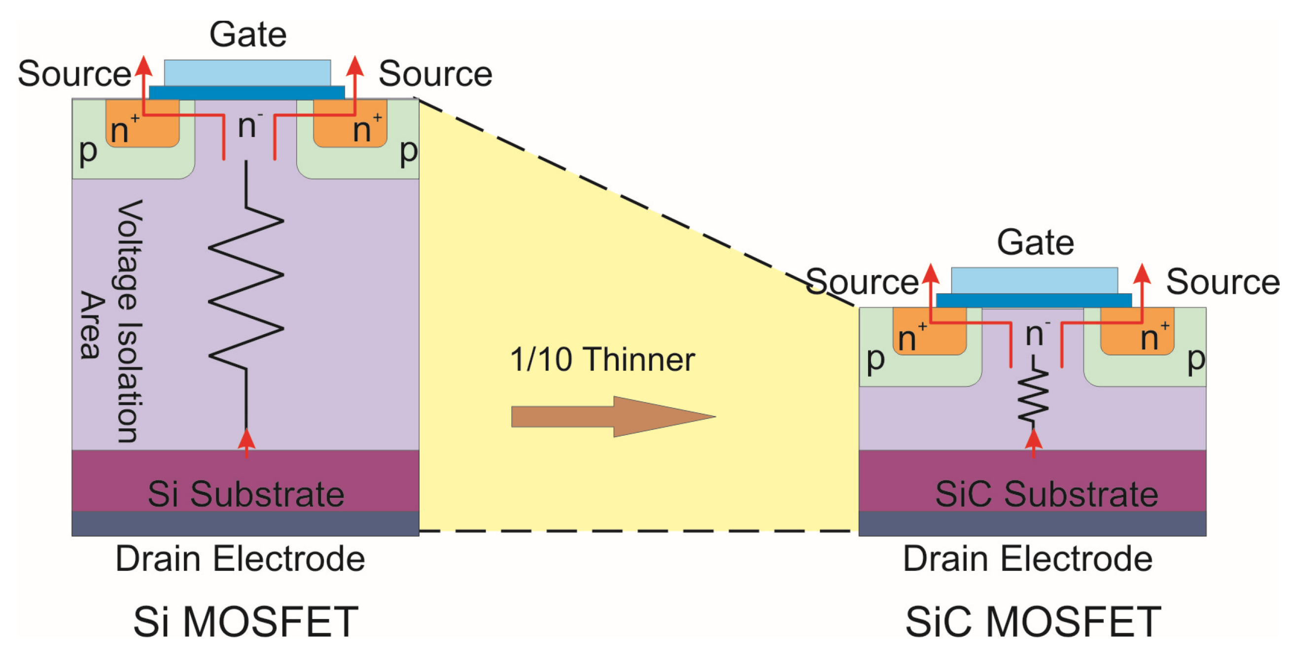
Figure 1. Comparison between Si and SiC.
JFETs have a rated voltage of 1200 V to 1700 V and a rated current of up to 48 A [7]. SiC MOSFETs are normally off power devices. In the MOSFET, the gate is insulated because there is an oxide layer between the gate and the drain. Practically no current passes from gate to source. On the other hand, generally, JFET has a reverse polarized pn junction that causes leakage current from gate to source. This causes the device to be normally on, unlike MOSFETs. Since SiC JFET is a normally on device, the negative voltage must be applied between the gate and source for the device to be off. The main disadvantage of normally on JFET is that negative voltage can cause a short circuit in the drive part of the device. For this reason, it is not preferred to be used in power electronics circuits [8].
To eliminate the disadvantage of SiC JFETs caused by the driver circuit, a SiC cascode JFET structure was created by connecting a Si MOSFET in series with the device. Here, the serial MOSFET has low conduction resistance [9][10]. This structure has the JFET’s conduction characteristics and the driving characteristics of Si MOSFET. However, due to high di/dt and dv/dt, high-frequency oscillations occur between the Si MOSFET’s parasitic capacitance and the circuit path’s leakage inductance [9]. These high-frequency oscillations can be avoided by using a snubber circuit [11]. The driving voltage of SiC cascode JFET has a wide range. Another advantage of SiC cascode JFET is that it can be used without changing the driving circuit of the Si device.
Due to their superior high efficiency, safety, cleanliness, and quick heating over conventional heating processes, domestic induction heating systems (DIHS) are becoming more and more popular on the market. In DIHS, when SiC power devices are used instead of Si, the total volume of the system decreases and power density and circuit efficiency increase [12][13][14][15][16].
2. Evaluation of Wide-Bandgap Semiconductors for High-Performance Domestic Induction Heating
The use of IH technology in home appliances first started with MOSFET in half -bridge (HB) and full-bridge (FB) topologies. In the following years, with the discovery of the high voltage value MOSFET, the lower-cost single-switched quasi-resonant (SSQR) topology was used in home applications [12][14].
With the development of the IGBT with low conduction resistance, the efficiency of topologies has increased [17]. In IH systems, the system’s efficiency is increased by using resonance topologies in which switching power losses do not occur or are reduced [18]. In IH systems, serial resonant (SR), FB, HB, and SSQR topologies are commonly used [19][20]. Figure 2 shows the topologies and power devices used in domestic IH systems over the years. The FB topology is suitable for industrial IH systems with an output power higher than 5 kW. In domestic IH systems, low-cost SSQR topology is up to 2 kW, and HB topology is used in a cost-performance balance of up to 5 kW [21].
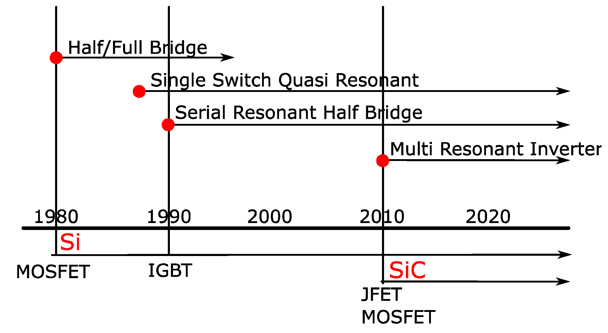
Figure 2. Circuit topologies and power devices used in domestic IH systems.
There are some disadvantages to SR HB topology, commonly realized with Si IGBT in DIHS [22]. These can be listed as follows:
-
Circuit volume cannot be reduced since IGBTs cannot be operated above 100 kHz;
-
Semiconductor power devices with wide bandwidth can operate at high voltages;
-
Nonferromagnetic materials cannot be heated because of the IGBT’s switching frequency, and voltage values are not high enough.
When SiC power devices are used instead of Si in IH applications, the above disadvantages are eliminated. As a result, the system’s total volume decreases and power density and circuit efficiency increase. In addition to those advantages, nonferromagnetic materials can be heated using SiC power devices [12][13][14][15][16].
Various studies have been conducted on using WBG devices in IH systems, as summarized in Table 1 [2][12][14][15][22][23][24][25][26][27][28][29][30][31][32]. In these studies, a single WBG device was mostly examined. In a limited number of studies, Si and WBG devices were examined comparatively.
Table 1. Survey of IH with WBG devices.
| Reference | Topology | Si | Si | SiC | SiC | SiC | SiC |
|---|---|---|---|---|---|---|---|
| IGBT | MOSFET | MOSFET | BJT | JFET | Cascode JFET | ||
| [23] | FB | X | |||||
| [2] | FB | X | |||||
| [24] | HB + FB | X | |||||
| [25] | FB | X | |||||
| [26] | CSRI | X | |||||
| [27] | SS QR | X | X | ||||
| [28] | QR | X | |||||
| [12] | FB | X | |||||
| [14] | SR HB | X | |||||
| [15] | FB | X | X | ||||
| [29] | SR FB | X | X | ||||
| [30] | LLC | X | X | X | |||
| [31] | Boost HB | X | X | ||||
| [32] | HB | X | |||||
| [33] | HB | X | X | X | X | ||
| PS | HB | X | X | X |
PS: Present Study.
Si and SiC MOSFETs were compared in FB topology used for surface hardening of irregular cylindrical parts. It has been observed that the turn-off power loss of SiC MOSFET is less than that of Si MOSFET, and the power loss of turn-on is decreased by 90% [14]. To verify the proposed multi-modulation technique in which a QR AC-AC topology was used, SiC JFET with a high voltage value was used in [12]. SiC JFET was used to achieve high performance and efficiency in the multi-output IH system realized with an FB AC-AC topology [12].
The behavior of the Si and SiC MOSFETs realized with SR FB topology has been investigated. It has been observed that the turn-off time of SiC MOSFET is 10 times lower than Si MOSFET [15]. SiC MOSFET is operated at a switching frequency of 400 kHz realized with an FB topology to separate foreign metal materials. In this case, the heatsink volume has decreased by 78% [33].
The switches’ power losses are investigated using Si IGBT, Si MOSFET, and SiC MOSFET, in which LLC topology with resonance is used. It has been observed that the lowest power loss is in SiC MOSFET [2][29]. The circuit’s efficiency and performance have been investigated using a three-phase SiC module in a new IH power supply using an interleaved resonance booster topology. The efficiencies of IH systems realized with HB and FB topologies using the SiC power module have been examined. Si IGBT module and SiC MOSFET module are used in high frequency [24]. It has been observed that the efficiency of the circuit increases with the SiC module [30]. The conduction and switching losses of SiC JFET and Si IGBT realized with a SS QR topology have been investigated [27]. SiC MOSFET is operated with FB topology at high frequency and power [25]. SiC cascode JFET is used in the domestic IH, which is realized with SR HB topology [34].
Details of the comparative studies are given in Table 2 [15][22][27][29][30]. In these studies, Si devices and SiC devices were compared in general. Although all of the studies have been examined from different aspects, the system efficiency has been examined in all except [27]. It is seen that the SiC cascode JFET, which is a combination of the superior features of the Si MOSFET and SiC JFET devices, is not compared with other devices in DIHS. As a result, the lack of comparison using the SiC cascode JFET device in the literature is seen as a research gap.
Table 2. Comparative studies.
| Ref. | Device | Topology | Analyses | ||||||
|---|---|---|---|---|---|---|---|---|---|
| Type | η | Voltage | Current | Pn | fSW | Type | Frequency | ||
| (%) | (V) | (A) | (kW) | (kHz) | |||||
| [15] | Si MOSFET | 97.3 | 1200 | 29 | 5 | 100 | FB | Constant | tOFF, tON, |
| 2Si MOSFET | 98 | 1200 | 24 | POFF, PON, | |||||
| SiC MOSFET | 99.2 | 1200 | 33 | PT, η | |||||
| [30] | Si IGBT | 95.2 | 1200 | 100 | 2.6 | 32 | Boost HB | Constant | POFF, PT, |
| SiC MOSFET | 97.2 | 1200 | 120 | η | |||||
| [27] | Si IGBT | N/A | 1200 | 30 | 2-1 | 21.3–314 | SSQR | Variable | VON, tOFF, |
| SiC JFET-nON | N/A | 1200 | 17 | T(°C) | |||||
| [29] | Si IGBT | 84 | 600 | 75 | 6 | 50 | LLC | Variable | PT, η |
| Si MOSFET | 91 | 600 | 65 | ||||||
| SiC MOSFET | 94 | 1200 | 45 | ||||||
| [22] | Si IGBT | 96.1 | N/A | N/ | 2 | 20 | HB | Constant | tOFF, POFF, |
| SiC MOSFET | 95.1 | 1200 | 42 | PON, PT, | |||||
| SiC BJT | 97.8 | 1200 | 50 | η,VON | |||||
| SiC JFET-nON | 96.3 | 1200 | 48 | ||||||
| SiC JFET-nOFF | 95.7 | 1200 | 30 | ||||||
| PS | Si IGBT | 97.3 | 600 | 48 | 0.2–1.8 | 125–45 | HB | Variable | PT, PCON, |
| SiC MOSFET | 97.6 | 650 | 27 | PSW, POFF, | |||||
| SiC MOSFET | 98.3 | 650 | 35 | PON, PBD, | |||||
| SiC MOSFET | 96.4 | 1200 | 28 | tOFF, tf, | |||||
| SiC MOSFET | 91.5 | 1200 | 16 | di/dt, VON, | |||||
| SiC cascode JFET | 98.1 | 650 | 62 | η, | |||||
| SiC cascode JFET | 99 | 1200 | 47 | ||||||
PS: Present Study.
References
- CREE. Application Considerations for Silicon Carbide MOSFETs under Power Appl. Notes. 2011. Available online: https://www.mouser.com/pdfDocs/Cree-Application-Considerations-for-Silicon-Carbide-MOSFETs.pdf (accessed on 11 December 2022).
- Sarnago, H.; Lucia, O.; Burdio, J.M. Interleaved resonant boost inverter featuring SiC module for high-performance induction heating. IEEE Trans. Power Electron. 2017, 32, 1018–1029.
- Prado, E.O.; Bolsi, P.C.; Sartori, H.C.; Pinheiro, J.R. An Overview about Si, Superjunction, SiC and GaN Power MOSFET Technologies in Power Electronics Applications. Energies 2022, 15, 5244.
- Górecki, P.; Górecki, K.; Kisiel, R.; Brzozowski, E.; Bar, J.; Guziewicz, M. Investigations of an Influence of the Assembling Method of the Die to the Case on Thermal Parameters of IGBTs. IEEE Trans. Compon. Packag. Manuf. Technol. 2021, 11, 1988–1996.
- Li, K.; Evans, P.; Johnson, M. SiC/GaN power semiconductor devices: A theoretical comparison and experimental evaluation under different switching conditions. IET Electr. Syst. Transp. 2018, 8, 3–11.
- Nakamura, T.; Nakano, Y.; Aketa, M.; Hanada, T. Recent Development and Future Prospects of Power SiC Devices. In Proceedings of the 2014 International Power Electronics Conference (IPEC-Hiroshima 2014-ECCE ASIA), Hiroshima, Japan, 18–21 May 2014; Volume 720, p. 2074.
- Nagy, I. Inverters-Resonant Converters; CRC: Boca Raton, FL, USA, 2002.
- Kotzea, S.; Debald, A.; Heuken, M.; Kalisch, H.; Vescan, A. Demonstration of a GaN-Based Vertical-Channel JFET Fabricated by Selective-Area Regrowth. IEEE Trans. Electron Devices 2018, 65, 5329–5336.
- Pittini, R.; Zhang, Z.; Andersen, M.A.E. SiC JFET Cascode Loss Dependency on the MOSFET Output Capacitance and Performance Comparison with Trench IGBTs. In Proceedings of the 2013 Twenty-Eighth Annual IEEE Applied Power Electronics Conference and Exposition (APEC), Long Beach, CA, USA, 17–21 March 2013; pp. 1287–1293.
- Josifović, I.; Popović-Gerber, J.; Ferreira, J.A. Improving SiC JFET switching behavior under influence of circuit parasitics. IEEE Trans. Power Electron. 2021, 27, 3843–3854.
- Haehre, K.; Meisser, M.; Denk, F.; Kling, R.; Heering, W. Switching Speed-Control of an Optimized Capacitor-Clamped Normally-on Silicon Carbide JFET Cascode. In Proceedings of the 15th International Power Electronics and Motion Control Conference (EPE/PEMC), Novi Sad, Serbia, 4–6 September 2012.
- Sarnago, H.; Lucia, O.; Mediano, A.; Burdio, J.M. Design and implementation of a high-efficiency multiple-output resonant converter for induction heating applications featuring wide bandgap devices. IEEE Trans. Power Electron. 2014, 29, 2539–2549.
- Ning, P.; Zhang, D.; Lai, R.; Jiang, D.; Wang, F.; Boroyevich, D.; Burgos, R.; Karimi, K.; Immanuel, V.D.; Solodovnik, E.V. High-temperature hardware: Development of a 10-kW high-temperature, high-power-density three-phase ac-dc-ac SiC converter. IEEE Ind. Electron. Mag. 2013, 7, 6–17.
- Esteve, V.; Jordan, J.; Sanchis-Kilders, E.; Dede, E.J.; Maset, E.; Ejea, J.B.; Ferreres, A. Comparative study of a single inverter bridge for dual-frequency induction heating using Si and SiC MOSFETs. IEEE Trans. Ind. Electron. 2015, 62, 1440–1450.
- Jordan, J.; Esteve, V.; Sanchis-Kilders, E.; Dede, E.J.; Maset, E.; Ejea, J.B.; Ferreres, A. A comparative performance study of a 1200 v Si and SiC MOSFET intrinsic diode on an induction heating inverter. IEEE Trans. Power Electron. 2014, 29, 2550–2562.
- Millan, J.; Godignon, P.; Perpina, X.; Perez-Tomas, A.; Rebollo, J. A survey of wide bandgap power semiconductor devices. IEEE Trans. Power Electron. 2014, 29, 2155–2163.
- Moreland, W.C. Induction Its Performance Development Problems. IEEE Trans. Ind. Appl. 1973, 1A-9, 81–85.
- Kazimierczuk, M.K.; Dariusz, C. Resonant Power Converters, 2nd ed.; John Wiley & Sons, Inc., Publication: Hoboken, NJ, USA, 2011.
- Dzieniakowski, M.A. Power Electronics Converters in Induction Heating—The Survey. In Proceedings of the 2017 Progress in Applied Electrical Engineering (PAEE), Koscielisko, Poland, 25–30 June 2017.
- Ozturk, M.; Zungor, F.; Emre, B.; Oz, B. Quasi Resonant Inverter Load Recognition Method. IEEE Access 2022, 10, 89376–89386.
- Vishnuram, P.; Ramachandiran, G.; Babu, T.S.; Nastasi, B. Induction heating in domestic cooking and industrial melting applications: A systematic review on modelling, converter topologies and control schemes. Energies 2021, 14, 6634.
- Sarnago, H.; Lucía, Ó.; Burdío, J.M. A Comparative Evaluation of SiC Power Devices for High-Performance Domestic Induction Heating. IEEE Trans. Ind. Electron. 2015, 62, 4795–4804.
- Shijo, T.; Kurachi, S.; Noda, Y.; Yamada, H.; Tanaka, T. A 400 kHz SiC-MOSFETs High-Frequency Inverter for Small-Foreign-Metal Particle Detection. In Proceedings of the 2016 IEEE 2nd Annual Southern Power Electronics Conference (SPEC), Auckland, New Zealand, 5–8 December 2016; pp. 3–7.
- Ogiwara, H.; Itoi, M.; Nakaoka, M. Highly Efficient High Frequency Inverter for Induction Heating Using SiC Power Module. In Proceedings of the 2016 IEEE International Power Electronics and Motion Control Conference (PEMC), Varna, Bulgaria, 25–28 September 2016; Volume 5, pp. 116–121.
- Komeda, S.; Tsuboi, Y.; Fujita, H. Inverter for Industrial Induction Heating Systems. In Proceedings of the 2014 International Power Electronics Conference (IPEC-Hiroshima 2014-ECCE ASIA), Hiroshima, Japan, 18–21 May 2014; pp. 1160–1165.
- Aunsborg, T.S.; Duun, S.B.; Munk-Nielsen, S.; Uhrenfeldt, C. Development of a current source resonant inverter for high current MHz induction heating. IET Power Electron. 2022, 15, 1–10.
- Gaudó, P.M.; Bernal, C.; Otín, A.; Burdío, J.M. Silicon carbide JFET resonant inverter for induction heating home appliances. In Proceedings of the IECON 2011-37th Annual Conference of the IEEE Industrial Electronics Society, Melbourne, VIC, Australia, 7–10 November 2011; pp. 2551–2556.
- Sarnago, H.; Lucia, O.; Mediano, A.; Burdio, J.M. A class-e direct AC-AC converter with multicycle modulation for induction heating systems. IEEE Trans. Ind. Electron. 2014, 61, 2521–2530.
- Valchev, V.C.; Mareva, D.J. Considerations for components selection of inverter for induction heating. In Proceedings of the 2016 25th International Scientific Conference Electronics (ET), Sozopol, Bulgaria, 12–14 September 2016; pp. 38–41.
- Mishima, T.; Morinaga, S.; Nakaoka, M. All-SiC power module-applied single-stage ZVS-PWM AC-AC converter for high-frequency induction heating. In Proceedings of the IECON 2015-41st Annual Conference of the IEEE Industrial Electronics Society, Yokohama, Japan, 9–12 November 2015; pp. 004211–004216.
- Laloya, E.; Lucia, O.; Concha, J.; Burdio, J.M. Experimental evaluation of dynamic load changes in flexible induction heating appliances. In Proceedings of the IECON 2014-40th Annual Conference of the IEEE Industrial Electronics Society, Dallas, TX, USA, 29 October–1 November 2014; pp. 3227–3232.
- Cha, K.-H.; Ju, C.-T.; Kim, R.-Y. Analysis and Evaluation of WBG Power Device in High Frequency Induction Heating Application. Energies 2020, 13, 5351.
- Shijo, T.; Kurachi, S.; Uchino, Y.; Noda, Y.; Yamada, H.; Tanaka, T. High-frequency induction heating for small-foreign-metal particle detection using 400 kHz SiC-MOSFETs inverter. In Proceedings of the 2017 IEEE Energy Conversion Congress and Exposition (ECCE), Cincinnati, OH, USA, 1–5 October 2017; pp. 5133–5138.
- Avellaned, J.; Bernal, C.; Otin, A.; Molina, P.; Burdio, J.M. Half-bridge resonant inverter with SiC cascode applied to domestic induction heating. In Proceedings of the 2013 Twenty-Eighth Annual IEEE Applied Power Electronics Conference and Exposition (APEC), Long Beach, CA, USA, 17–21 March 2013; pp. 122–127.
More
Information
Subjects:
Engineering, Electrical & Electronic
Contributors
MDPI registered users' name will be linked to their SciProfiles pages. To register with us, please refer to https://encyclopedia.pub/register
:
View Times:
886
Revisions:
2 times
(View History)
Update Date:
25 May 2023
Table of Contents


Notice
You are not a member of the advisory board for this topic. If you want to update advisory board member profile, please contact office@encyclopedia.pub.
OK
Confirm
Only members of the Encyclopedia advisory board for this topic are allowed to note entries. Would you like to become an advisory board member of the Encyclopedia?
Yes
No
${ textCharacter }/${ maxCharacter }
Submit
Cancel
Back
Comments
${ item }
|
${ item.createdUser.fullName }
${ item.createdAt }
${ item.vote }
${ item.reply }
Delete
${ reply.createdUser.fullName }
${ reply.createdAt }
${ reply.vote }
Delete
There is no reply to this comment~
${ item.replyTextCharacter }/${ item.replyMaxCharacter }
Submit
Cancel
More
No more~
There is no comment~
${ textCharacter }/${ maxCharacter }
Submit
Cancel
${ selectedItem.replyTextCharacter }/${ selectedItem.replyMaxCharacter }
Submit
Cancel
Confirm
Are you sure to Delete?
Yes
No