Your browser does not fully support modern features. Please upgrade for a smoother experience.
Please note this is an old version of this entry, which may differ significantly from the current revision.
Subjects:
Engineering, Electrical & Electronic
In the induction heating system, the power transferred to the output depends on the equivalent resistance of the load, and the resistance depends on the operating frequency. Due to the switching characteristics of wide-bandgap power semiconductor devices, an induction heating system can be operated at higher operating frequencies.
- induction cooking hobs
- resonant half bridge
- SiC cascode JFET
1. Introduction
The semiconductor materials used in power devices determine the current and voltage values of the devices. The features expected from semiconductor power devices are low thermal resistance, wide energy bandgap, and operation at high frequencies [1]. The low thermal resistance of the semiconductor power devices results in a shorter thermal time constant.
Operating the switches at high frequencies reduces the passive component sizes and the circuit volume. The operation of the circuit at high frequencies is possible with power devices with high electron drift velocity. Power devices with wide energy bandgap have thinner layers, low internal resistance, fewer power losses, and leakage currents, so they have higher package thermal resistances and can operate at higher voltages. The Si element is often preferred in power devices because of its stable and easy production. Silicon carbide (SiC) and gallium nitrate (GaN) are materials with wide bandgap (WBG) used in semiconductor power devices [2,3].
Silicon (Si) power devices have undergone many changes from the date they were first used to the present day. In terms of maximum voltage that can be applied, operating temperature, conduction, and switching properties, these devices are getting close to their theoretically permitted limits for the materials. State-of-the-art Si-insulated gate bipolar transistors (IGBTs) have a voltage rating of five kV because of their restricted performance, and switching speeds are still slow because of tail currents. In addition, most of the commercial Si-based devices currently have a maximum junction temperature below 175 °C. The thermal limitation is due to the liquid temperature of the solder layer. The thermal performance of the device is lower than soldering when sintering or gluing is used [4]. Obtaining converters with higher power densities is difficult because of these inherent physical constraints [5].
Along with the commercial production of wide-bandgap semiconductor devices, these devices have begun to be used in state-of-the-art power converters. In contrast to Si devices, WBG devices have a large breakdown electric field, a low conduction resistance, a high switching speed, and a high junction temperature tolerance. These properties affect the conversion’s efficiency, power density, output power, and reliability [3].
As a result of the advancement in SiC technology, SiC metal-oxide field-effect transistors (MOSFETs) operating at higher powers and with better temperature strength than Si MOSFET have been produced [6]. In SiC MOSFET, the thickness of the area holding the voltage is made 10 times thinner than Si MOSFET, as shown in Figure 1, while the additive density can be increased 10 times. In this way, the on-state resistance of the SiC MOSFET decreases to one percent of the resistance of the Si MOSFET with the same properties. Thus, the on-state resistance, the main disadvantage of Si MOSFETs, is reduced. Drive circuits must include protection against the uncontrolled operation of the device caused by environmental noise [5].
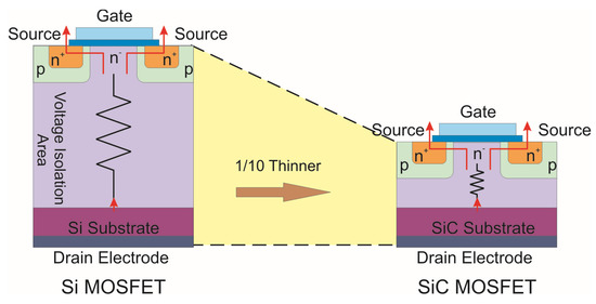
Figure 1. Comparison between Si and SiC.
JFETs have a rated voltage of 1200 V to 1700 V and a rated current of up to 48 A [7]. SiC MOSFETs are normally off power devices. In the MOSFET, the gate is insulated because there is an oxide layer between the gate and the drain. Practically no current passes from gate to source. On the other hand, generally, JFET has a reverse polarized pn junction that causes leakage current from gate to source. This causes the device to be normally on, unlike MOSFETs. Since SiC JFET is a normally on device, the negative voltage must be applied between the gate and source for the device to be off. The main disadvantage of normally on JFET is that negative voltage can cause a short circuit in the drive part of the device. For this reason, it is not preferred to be used in power electronics circuits [8].
To eliminate the disadvantage of SiC JFETs caused by the driver circuit, a SiC cascode JFET structure was created by connecting a Si MOSFET in series with the device. Here, the serial MOSFET has low conduction resistance [9,10]. This structure has the JFET’s conduction characteristics and the driving characteristics of Si MOSFET. However, due to high di/dt and dv/dt, high-frequency oscillations occur between the Si MOSFET’s parasitic capacitance and the circuit path’s leakage inductance [9]. These high-frequency oscillations can be avoided by using a snubber circuit [11]. The driving voltage of SiC cascode JFET has a wide range. Another advantage of SiC cascode JFET is that it can be used without changing the driving circuit of the Si device.
Due to their superior high efficiency, safety, cleanliness, and quick heating over conventional heating processes, domestic induction heating systems (DIHS) are becoming more and more popular on the market. In DIHS, when SiC power devices are used instead of Si, the total volume of the system decreases and power density and circuit efficiency increase [12,13,14,15,16].
2. Evaluation of Wide-Bandgap Semiconductors for High-Performance Domestic Induction Heating
The use of IH technology in home appliances first started with MOSFET in half -bridge (HB) and full-bridge (FB) topologies. In the following years, with the discovery of the high voltage value MOSFET, the lower-cost single-switched quasi-resonant (SSQR) topology was used in home applications [12,14].
With the development of the IGBT with low conduction resistance, the efficiency of topologies has increased [17]. In IH systems, the system’s efficiency is increased by using resonance topologies in which switching power losses do not occur or are reduced [18]. In IH systems, serial resonant (SR), FB, HB, and SSQR topologies are commonly used [19,20]. Figure 2 shows the topologies and power devices used in domestic IH systems over the years. The FB topology is suitable for industrial IH systems with an output power higher than 5 kW. In domestic IH systems, low-cost SSQR topology is up to 2 kW, and HB topology is used in a cost-performance balance of up to 5 kW [21].
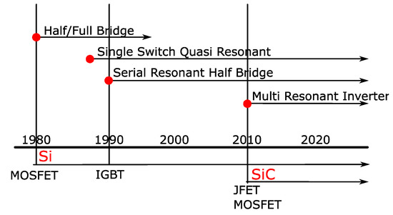
Figure 2. Circuit topologies and power devices used in domestic IH systems.
There are some disadvantages to SR HB topology, commonly realized with Si IGBT in DIHS [22]. These can be listed as follows:
-
Circuit volume cannot be reduced since IGBTs cannot be operated above 100 kHz;
-
Semiconductor power devices with wide bandwidth can operate at high voltages;
-
Nonferromagnetic materials cannot be heated because of the IGBT’s switching frequency, and voltage values are not high enough.
When SiC power devices are used instead of Si in IH applications, the above disadvantages are eliminated. As a result, the system’s total volume decreases and power density and circuit efficiency increase. In addition to those advantages, nonferromagnetic materials can be heated using SiC power devices [12,13,14,15,16].
Various studies have been conducted on using WBG devices in IH systems, as summarized in Table 1 [2,12,14,15,22,23,24,25,26,27,28,29,30,31,32]. In these studies, a single WBG device was mostly examined. In a limited number of studies, Si and WBG devices were examined comparatively.
Table 1. Survey of IH with WBG devices.
| Reference | Topology | Si | Si | SiC | SiC | SiC | SiC |
|---|---|---|---|---|---|---|---|
| IGBT | MOSFET | MOSFET | BJT | JFET | Cascode JFET | ||
| [23] | FB | X | |||||
| [2] | FB | X | |||||
| [24] | HB + FB | X | |||||
| [25] | FB | X | |||||
| [26] | CSRI | X | |||||
| [27] | SS QR | X | X | ||||
| [28] | QR | X | |||||
| [12] | FB | X | |||||
| [14] | SR HB | X | |||||
| [15] | FB | X | X | ||||
| [29] | SR FB | X | X | ||||
| [30] | LLC | X | X | X | |||
| [31] | Boost HB | X | X | ||||
| [32] | HB | X | |||||
| [33] | HB | X | X | X | X | ||
| PS | HB | X | X | X |
PS: Present Study.
Si and SiC MOSFETs were compared in FB topology used for surface hardening of irregular cylindrical parts. It has been observed that the turn-off power loss of SiC MOSFET is less than that of Si MOSFET, and the power loss of turn-on is decreased by 90% [14]. To verify the proposed multi-modulation technique in which a QR AC-AC topology was used, SiC JFET with a high voltage value was used in [12]. SiC JFET was used to achieve high performance and efficiency in the multi-output IH system realized with an FB AC-AC topology [12].
The behavior of the Si and SiC MOSFETs realized with SR FB topology has been investigated. It has been observed that the turn-off time of SiC MOSFET is 10 times lower than Si MOSFET [15]. SiC MOSFET is operated at a switching frequency of 400 kHz realized with an FB topology to separate foreign metal materials. In this case, the heatsink volume has decreased by 78% [33].
The switches’ power losses are investigated using Si IGBT, Si MOSFET, and SiC MOSFET, in which LLC topology with resonance is used. It has been observed that the lowest power loss is in SiC MOSFET [2,29]. The circuit’s efficiency and performance have been investigated using a three-phase SiC module in a new IH power supply using an interleaved resonance booster topology. The efficiencies of IH systems realized with HB and FB topologies using the SiC power module have been examined. Si IGBT module and SiC MOSFET module are used in high frequency [24]. It has been observed that the efficiency of the circuit increases with the SiC module [30]. The conduction and switching losses of SiC JFET and Si IGBT realized with a SS QR topology have been investigated [27]. SiC MOSFET is operated with FB topology at high frequency and power [25]. SiC cascode JFET is used in the domestic IH, which is realized with SR HB topology [34].
Details of the comparative studies are given in Table 2 [15,22,27,29,30]. In these studies, Si devices and SiC devices were compared in general. Although all of the studies have been examined from different aspects, the system efficiency has been examined in all except [27]. It is seen that the SiC cascode JFET, which is a combination of the superior features of the Si MOSFET and SiC JFET devices, is not compared with other devices in DIHS. As a result, the lack of comparison using the SiC cascode JFET device in the literature is seen as a research gap.
This entry is adapted from the peer-reviewed paper 10.3390/en16103987
This entry is offline, you can click here to edit this entry!