Your browser does not fully support modern features. Please upgrade for a smoother experience.
Submitted Successfully!
 +1 credit
Thank you for your contribution! You can also upload a video entry or images related to this topic.
For video creation, please contact our Academic Video Service.
| Version | Summary | Created by | Modification | Content Size | Created at | Operation |
|---|---|---|---|---|---|---|
| 1 | Jiayang Wu | -- | 1359 | 2023-02-13 07:37:16 | | | |
| 2 | Conner Chen | + 4 word(s) | 1363 | 2023-02-13 09:03:27 | | |
Video Upload Options
We provide professional Academic Video Service to translate complex research into visually appealing presentations. Would you like to try it?
Cite
If you have any further questions, please contact Encyclopedia Editorial Office.
Jia, L.; Wu, J.; Zhang, Y.; Qu, Y.; Jia, B.; Moss, D.J. Two-Dimensional Materials in Nonlinear Optical Devices. Encyclopedia. Available online: https://encyclopedia.pub/entry/41139 (accessed on 26 July 2026).
Jia L, Wu J, Zhang Y, Qu Y, Jia B, Moss DJ. Two-Dimensional Materials in Nonlinear Optical Devices. Encyclopedia. Available at: https://encyclopedia.pub/entry/41139. Accessed July 26, 2026.
Jia, Linnan, Jiayang Wu, Yuning Zhang, Yang Qu, Baohua Jia, David J. Moss. "Two-Dimensional Materials in Nonlinear Optical Devices" Encyclopedia, https://encyclopedia.pub/entry/41139 (accessed July 26, 2026).
Jia, L., Wu, J., Zhang, Y., Qu, Y., Jia, B., & Moss, D.J. (2023, February 13). Two-Dimensional Materials in Nonlinear Optical Devices. In Encyclopedia. https://encyclopedia.pub/entry/41139
Jia, Linnan, et al. "Two-Dimensional Materials in Nonlinear Optical Devices." Encyclopedia. Web. 13 February, 2023.
Copy Citation
All-optical signal processing based on nonlinear optical devices is promising for ultrafast information processing in optical communication systems. Recent advances in two-dimensional (2D) layered materials with unique structures and distinctive properties have opened up new avenues for nonlinear optics and the fabrication of related devices with high performance.
third-order optical nonlinearity
2D materials
telecommunications band
1. Introduction
All-optical signal processing based on nonlinear optical devices is an attractive technique for ultrahigh speed signal processing for optical communication systems. It offers broad operation bandwidths, ultra-high processing speeds, together with low power consumption and potentially reduced footprint and cost. Integrated nonlinear optical photonic chips have been based on a few key materials including silicon (Si) [1][2][3], doped silica (SiO2) [4][5], silicon nitride (Si3N4) [6][7], aluminum gallium arsenide (AlGaAs) [8][9][10], and chalcogenide glasses [11][12]. These have enabled a wide range of devices from Raman amplification and lasing [13][14][15], wavelength conversion [5][12][16][17][18], optical logic gates [19][20][21][22], and optical frequency comb generation [23][24][25][26], to optical temporal cloaking [27], quantum entangling [28][29][30], and many others. Despite their success, no platform is perfect—they all have limitations, such as a relatively small Kerr nonlinearity (n2) (e.g., for Si3N4) or high two photon absorption (for silicon in the telecommunications band), resulting in a low nonlinear figure of merit (FOM = n2/(λβTPA), with n2 and βTPA denoting the effective Kerr coefficient and two-photon absorption (TPA) coefficient of the waveguides, respectively, and λ the light wavelength).
To overcome these limitations, newly emerging materials have attracted significant attention, particularly two-dimensional (2D)-layered materials, such as graphene [31][32][33], GO [34][35][36], TMDCs [37][38][39][40], h-BN [41][42][43], and BP [44][45][46], where their atomically thin nature yields unique and superior properties. Compared with bulk materials, the 2D materials possess surfaces that are free of dangling bonds due to their weak out-of-plane van der Waals interactions [32][37]. In particular, their properties are highly dependent on the number of atomic layers—not only is their optical bandgap highly layer thickness dependent but they can also exhibit an indirect-to-direct bandgap transition (and the reverse), which provides powerful ways in which to tune their optical responses [37][46][47][48]. Further, their broadband photoluminescence and ultrahigh carrier mobility are highly attractive features for photonic and optoelectronic applications [33][49][50][51][52][53]. The unique photon-excited exciton and valley-selective properties of monolayer TMDCs and their heterostructures are promising for the development of future spintronic and quantum computing devices [37][38]. Finally, in addition to their linear optical properties, 2D materials exhibit remarkable nonlinear optical properties including strong saturable absorption (SA) [54][55][56][57], a giant Kerr nonlinearity [58][59][60][61][62], and prominent second- (SHG) and third-harmonic generation (THG) [44][63][64][65], opening up new avenues for high-performance nonlinear optical devices.
In contrast to the second-order optical nonlinearity that only exists in non-centrosymmetric materials, the third-order susceptibility is present in all materials, which gives rise to a rich variety of processes, including four-wave mixing (FWM), self-phase modulation (SPM), cross-phase modulation (XPM), THG, two-photon absorption (TPA), SA, stimulated Raman scattering, and many others. These third-order nonlinear optical processes are quasi-instantaneous with ultrafast response times on the order of femtoseconds [66]. This has motivated ultrafast all-optical signal generation and processing for telecommunications, spectroscopy, metrology, sensing, quantum optics, and many other areas [67][68].
2. 2D Materials
The past decade has witnessed an enormous surge in research on layered 2D materials—many have been discovered and synthesized with a wide range of properties. This section briefly introduce some key 2D materials such as graphene, GO, TMDCs, h-BN, and BP as shown in Figure 1 and discuss their electrical and optical properties.
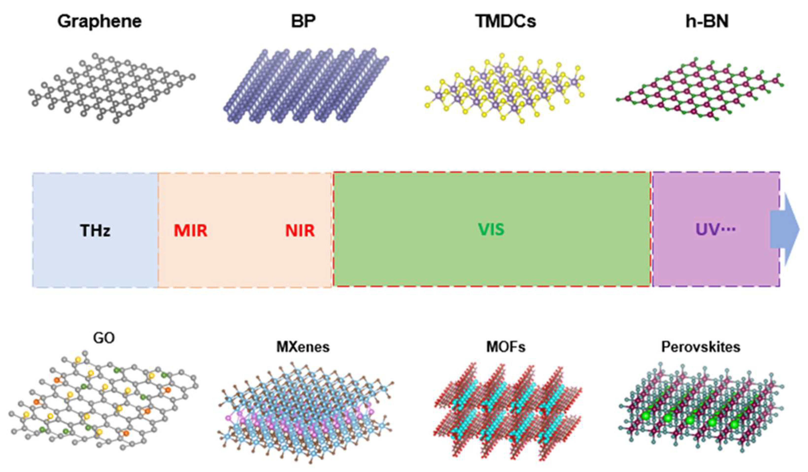
Figure 1. Illustration of typical 2D-layered materials.
2.1. Graphene and Graphene Oxide
Graphene, and its derivative, graphene oxide (GO), have been intensely studied due to their excellent mechanical, electrical, and optical properties [33][69][70]. Graphene has a gapless band structure, in which the conduction and valence bands meet at the K point of Brillouin zone, resulting in its semimetal nature [31][44][71]. In contrast, GO is an electronically hybrid material, featuring both conducting π-states from sp2 carbon sites and a large energy gap between the σ-states of its sp3-bonded carbons [34][72]. Their unique band structures result in novel electrical and optical properties, where for graphene, for example, the electrons and holes act as massless Dirac fermions resulting in extremely high carrier mobilities (>105 cm2/Vs) even under ambient conditions [31]. In contrast, GO exhibits a band gap that is tunable by adjusting the degree of reduction, which in turn affects the electric and optical properties. In addition, GO exhibits fluorescence in the near-infrared (NIR), visible and ultraviolet regions [34][35][36], which is very promising for light emitting devices. Moreover, the excellent nonlinear optical properties of both materials have been reported, including strong saturable absorption (SA) [73][74], a giant optical Kerr nonlinearity [58][59], leading to efficient self-phase modulation [75], FWM [76][77], as well as high harmonic generation [63].
2.2. Transition Metal Dichalcogenides
Transition metal dichalcogenides (TMDCs) with the formula of MX2 (where M is a transition metal and X is a chalcogen), is another widely studied family of 2D materials. Different to the semimetal graphene, monolayer TMDCs, such as MoS2, MoSe2, WS2, and WSe2, are typically semiconductors that have bandgaps from 1 eV to 2.5 eV, covering the spectral range from the near infrared to the visible region [37][38]. Moreover, TMDCs can exhibit a transition from direct- to indirect-bandgaps with increasing film thickness, resulting in strongly thickness-tunable optical and electrical properties. For instance, MoS2 exhibits layer-dependent photoluminescence, with monolayer films showing a much stronger photoluminescence [78]. Monolayer hexagonal TMDCs also exhibit unique band structure valley-dependent properties, such as valley coherence and valley-selective circular dichroism [37][79], offering new prospects for novel applications in optical computing and information processing. For the nonlinear optical properties, TMDCs with odd numbers of layers have no inversion symmetry, and so exhibit a non-zero second-order (and higher even-order) nonlinearities that are absent in graphene and even-layer TMDCs [44][64]. Recently, noble metal TMDCs, including PdSe2 and PtSe2, and PdTe2, have also attracted increasing interest in the fabrication of high performance electronic and optical devices, such as ultra-broadband photodetectors [39][40] as well as mode-locked lasers [80].
2.3. Black Phosphorus
Black phosphorus (BP) is another attractive single element 2D-layered material which has been widely studied. It has a puckered crystal structure, yielding a strong in-plane anisotropy in its physical properties in the “armchair” and “zigzag” directions, opening new avenues for anisotropic electronic and optoelectronic devices [44][45][81]. Moreover, BP is a semiconductor that features a layer thickness-dependent direct bandgap from 0.3 eV (bulk) to 2.0 eV (monolayer), bridging the gap between the zero-bandgap graphene and large-bandgap TMDCs [48][81]. This broad bandgap tunability is very suitable for the photodetection and photonic applications from the visible to mid-infrared spectra regions [46][47][82]. For the nonlinear optical properties, the layer thickness tunable and polarization-dependent THG and optical Kerr nonlinearity have been demonstrated recently [81][83]. Broadband SA has also been observed in BP, demonstrating its strong potential for ultrafast pulsed lasers [84][85][86].
2.4. Other Emerging 2D Materials
A wide range of other novel 2D low-dimensional materials have been investigated, including h-BN, MXenes, perovskites, as well as MOFs, which greatly enriches the family of 2D materials. h-BN is an electrical insulator with a large bandgap of around 5.9 eV [41][87] making h-BN a candidate for ultraviolet light applications. It also has an ultra-flat surface as well as excellent resistance to oxidation and corrosion, which are both highly useful as a dielectric or capping layer to protect the active materials or devices from degradation [41].
MXenes belong to another family of 2D materials, including 2D transition metal carbides, nitrides, and carbonitrides. Typically, the electronic structure of MXenes can be tuned by varying the surface functional groups. For instance, nonterminated Ti3C2 theoretically resembles a typical semimetal with a finite density of states at the Fermi level, whereas it can transition to a semiconductor when terminated with surface groups, such as OH and F groups [88]. MXnens also exhibit superior optical properties, such as a high optical transmittance of visible light (>97% per nm) [38][89], and excellent nonlinear optical properties [57].
Organometal-halide perovskites have a general formula of ABX3, where typically A = CH3NH3+, B = Pb2+, and X = I−, Br−, Cl− or mixtures [90]. Due to their prominent photovoltaic features and luminescence properties, organometal-halide perovskite semiconductors have been widely used to design high performance solar cells as well as light-emitting diodes [51][52][53]. Metal-organic frameworks (MOFs) are organic–inorganic hybrid porous crystalline materials with metal ions or metal-oxo clusters coordinated with organic linkers [91][92]. Thanks to this unique structure, 2D MOFs exhibit enhanced photo-physical behaviour and are promising for various applications, from light emission and sensing to nonlinear optical applications [93][94].
References
- Leuthold, J.; Koos, C.; Freude, W. Nonlinear silicon photonics. Nat. Photonics 2010, 4, 535–544.
- Xia, F.; Sekaric, L.; Vlasov, Y. Ultracompact optical buffers on a silicon chip. Nat. Photonics 2007, 1, 65–71.
- Foster, M.A.; Turner, A.C.; Sharping, J.E.; Schmidt, B.S.; Lipson, M.; Gaeta, A.L. Broad-band optical parametric gain on a silicon photonic chip. Nature 2006, 441, 960–963.
- Razzari, L.; Duchesne, D.; Ferrera, M.; Morandotti, R.; Chu, S.; Little, B.E.; Moss, D.J. CMOS-compatible integrated optical hyper-parametric oscillator. Nat. Photonics 2009, 4, 41–45.
- Ferrera, M.; Razzari, L.; Duchesne, D.; Morandotti, R.; Yang, Z.; Liscidini, M.; Sipe, J.E.; Chu, S.; Little, B.E.; Moss, D.J. Low-power continuous-wave nonlinear optics in doped silica glass integrated waveguide structures. Nat. Photonics 2008, 2, 737–740.
- Gaeta, A.L.; Lipson, M.; Kippenberg, T.J. Photonic-chip-based frequency combs. Nat. Photonics 2019, 13, 158–169.
- Demongodin, P.; Dirani, H.E.; Lhuillier, J.; Crochemore, R.; Kemiche, M.; Wood, T.; Callard, S.; Rojo-Romeo, P.; Sciancalepore, C.; Grillet, C. Ultrafast saturable absorption dynamics in hybrid graphene/Si3N4 waveguides. APL Photonics 2019, 4, 076102.
- Aitchison, J.S.; Hutchings, D.C.; Kang, J.U.; Stegeman, G.I.; Villeneuve, A. The nonlinear optical properties of AlGaAs at the half band gap. IEEE J. Quantum Electron. 1997, 33, 341–348.
- Kawashima, H.; Tanaka, Y.; Ikeda, N.; Sugimoto, Y.; Hasama, T.; Ishikawa, H. Optical Bistable Response in AlGaAs-Based Photonic Crystal Microcavities and Related Nonlinearities. IEEE J. Quantum Electron. 2008, 44, 841–849.
- Xie, W.; Chang, L.; Shu, H.; Norman, J.C.; Peters, J.D.; Wang, X.; Bowers, J.E. Ultrahigh-Q AlGaAs-on-insulator microresonators for integrated nonlinear photonics. Opt. Express 2020, 28, 32894–32906.
- Nicoletti, E.; Bulla, D.; Luther-Davies, B.; Gu, M. Generation of lambda/12 nanowires in chalcogenide glasses. Nano Lett. 2011, 11, 4218–4221.
- Eggleton, B.J.; Luther-Davies, B.; Richardson, K. Chalcogenide photonics. Nat. Photonics 2011, 5, 141–148.
- Liang, T.K.; Tsang, H.K. Efficient Raman amplification in silicon-on-insulator waveguides. Appl. Phys. Lett. 2004, 85, 3343–3345.
- Yamashita, D.; Asano, T.; Susumu, N.; Takahashi, Y. Strongly asymmetric wavelength dependence of optical gain in nanocavity-based Raman silicon lasers. Optica 2018, 5, 1256–1263.
- Zhang, Y.; Zhong, K.; Tsang, H.K. Raman Lasing in Multimode Silicon Racetrack Resonators. Laser Photonics Rev. 2020, 15, 2000336.
- Salem, R.; Foster, M.A.; Turner, A.C.; Geraghty, D.F.; Lipson, M. Signal regeneration using low-power four-wave mixing on silicon chip. Nat. Photonics 2008, 2, 35–38.
- Mathlouthi, W.; Rong, H.; Paniccia, M. Characterization of efficient wavelength conversion by four-wave mixing in sub-micron silicon waveguides. Opt. Express 2008, 16, 16735–16745.
- Frigg, A.; Boes, A.; Ren, G.; Nguyen, T.G.; Choi, D.-Y.; Gees, S.; Moss, D.; Mitchell, A. Optical frequency comb generation with low temperature reactive sputtered silicon nitride waveguides. APL Photonics 2020, 5, 011302.
- Li, F.; Vo, T.D.; Husko, C.; Pelusi, M.; Xu, D.-X.; Densmore, A.; Ma, R.; Janz, S.; Eg-gleton, B.J.; Moss, D.J. All-optical XOR logic gate for 40 Gb/s DPSK signals via FWM in a silicon nanowire. Opt. Express 2011, 19, 20364–20371.
- Gao, S.; Wang, X.; Xie, Y.; Hu, P.; Yan, Q. Reconfigurable dual-channel all-optical logic gate in a silicon waveguide using polarization encoding. Opt. Lett. 2015, 40, 1448–1451.
- Soref, R.; De Leonardis, F.; Ying, Z.; Passaro, V.M.N.; Chen, R.T. Silicon-Based Group-IV O-E-O Devices for Gain, Logic, and Wavelength Conversion. ACS Photonics 2020, 7, 800–811.
- Monat, C.; Grillet, C.; Collins, M.; Clark, A.; Schroeder, J.; Xiong, C.; Li, J.; O’Faolain, L.; Krauss, T.F.; Eggleton, B.J. Integrated optical auto-correlator based on third-harmonic generation in a silicon photonic crystal waveguide. Nat. Commun. 2014, 5, 3246.
- Wu, J.; Xu, X.; Nguyen, T.G.; Chu, S.T.; Little, B.E.; Morandotti, R.; Mitchell, A.; Moss, D.J. RF Photonics: An Optical Microcombs’ Perspective. IEEE J. Sel. Top. Quantum Electron. 2018, 24, 1–20.
- Xu, X.; Wu, J.; Nguyen, T.G.; Chu, S.T.; Little, B.E.; Morandotti, R.; Mitchell, A.; Moss, D.J. Broadband RF Channelizer Based on an Integrated Optical Frequency Kerr Comb Source. J. Lightwave Technol. 2018, 36, 4519–4526.
- Xu, X.; Tan, M.; Wu, J.; Morandotti, R.; Mitchell, A.; Moss, D.J. Microcomb-Based Photonic RF Signal Processing. IEEE Photonics Technol. Lett. 2019, 31, 1854–1857.
- Corcoran, B.; Corcoran, B.; Tan, M.; Xu, X.; Boes, A.; Wu, J.; Nguyen, T.G.; Chu, S.T. Ultra-dense optical data transmission over standard fibre with a single chip source. Nat. Commun. 2020, 11, 2568.
- Fridman, M.; Farsi, A.; Okawachi, Y.; Gaeta, A.L. Demonstration of temporal cloaking. Nature 2012, 481, 62–65.
- Reimer, C.; Kues, M.; Roztocki, P.; Wetzel, B.; Grazioso, F.; Little, B.E.; Chu, S.T.; Johnston, T.; Bromberg, Y.; Caspani, L.; et al. Generation of multiphoton entangled quantum states by means of integrated frequency combs. Science 2016, 351, 1176–1180.
- Kues, M.; Reimer, C.; Roztocki, P.; Cortés, L.R.; Sciara, S.; Wetzel, B.; Zhang, Y.; Cino, A.; Chu, S.T.; Little, B.E.; et al. On-chip generation of high-dimensional entangled quantum states and their coherent control. Nature 2017, 546, 622–626.
- Caspani, L.; Xiong, C.; Eggleton, B.J.; Bajoni, D.; Liscidini, M.; Galli, M.; Morandotti, R.; Moss, D.J. Integrated sources of photon quantum states based on nonlinear optics. Light Sci. Appl. 2017, 6, e17100.
- Geim, A.K.; Novoselov, K.S. The rise of graphene. Nat. Mater. 2007, 6, 183–191.
- Yang, T.; Lin, H.; Zheng, X.; Loh, K.P.; Jia, B. Tailoring pores in graphene-based materials: From generation to applications. J. Mater. Chem. A 2017, 5, 16537–16558.
- Bolotin, K.I.; Sikes, K.J.; Hone, J.; Stormer, H.L.; Kim, P. Temperature-dependent transport in suspended graphene. Phys. Rev. Lett. 2008, 101, 096802.
- Loh, K.P.; Bao, Q.; Eda, G.; Chhowalla, M. Graphene oxide as a chemically tunable platform for optical applications. Nat. Chem. 2010, 2, 1015–1024.
- Ghofraniha, N.; Conti, C. Graphene oxide photonics. J. Opt. 2019, 21, 053001.
- Luo, Z.; Vora, P.M.; Mele, E.J.; Johnson, A.T.C.; Kikkawa, J.M. Photoluminescence and band gap modulation in graphene oxide. Appl. Phys. Lett. 2009, 94, 111909.
- Tian, H.; Chin, M.L.; Najmaei, S.; Guo, Q.; Xia, F.; Wang, H.; Dubey, M. Optoelectronic devices based on two-dimensional transition metal dichalcogenides. Nano Res. 2016, 9, 1543–1560.
- Tan, T.; Jiang, X.; Wang, C.; Yao, B.; Zhang, H. 2D Material Optoelectronics for Information Functional Device Applications: Status and Challenges. Adv. Sci. 2020, 7, 2000058.
- Liang, Q.; Wang, Q.; Zhang, Q.; Wei, J.; Lim, S.X.; Zhu, R.; Hu, J.; Wei, W.; Lee, C.; Sow, C. High-Performance, Room Temperature, Ultra-Broadband Photodetectors Based on Air-Stable PdSe2. Adv. Mater. 2019, 31, e1807609.
- Pi, L.; Pi, L.; Li, L.; Liu, K.; Zhang, Q.; Li, H.; Zhai, T. Recent Progress on 2D Noble-Transition-Metal Dichalcogenides. Adv. Funct. Mater. 2019, 29, 1904932.
- Zhang, K.; Feng, Y.; Wang, F.; Yang, Z.; Wang, J. Two dimensional hexagonal boron nitride (2D-hBN): Synthesis, properties and applications. J. Mater. Chem. C 2017, 5, 11992–12022.
- Tran, T.T.; Bray, K.; Ford, M.J.; Toth, M.; Aharonovich, I. Quantum emission from hexagonal boron nitride monolayers. Nat. Nanotechnol. 2016, 11, 37–41.
- Caldwell, J.D.; Aharonovich, I.; Cassabois, G.; Edgar, J.H.; Gil, B.; Basov, D.N. Photonics with hexagonal boron nitride. Nat. Rev. Mater. 2019, 4, 552–567.
- Autere, A.; Jussila, H.; Dai, Y.; Wang, Y.; Lipsanen, H.; Sun, Z. Nonlinear Optics with 2D Layered Materials. Adv. Mater. 2018, 30, 1705963.
- Qiao, J.; Kong, X.; Hu, Z.-X.; Yang, F.; Ji, W. High-mobility transport anisotropy and linear dichroism in few-layer black phosphorus. Nat. Commun. 2014, 5, 4475.
- Yuan, H.; Liu, X.; Afshinmanesh, F.; Li, W.; Xu, G.; Sun, J.; Lian, B.; Curto, A.G.; Ye, G.; Hikita, Y.; et al. Polarization-sensitive broadband photodetector using a black phosphorus vertical p–n junction. Nat. Nanotechnol. 2015, 10, 707–713.
- Guo, Q.; Pospischil, A.; Bhuiyan, M.; Jiang, H.; Tian, H.; Farmer, D.; Deng, B.; Li, C.; Han, S.-J.; Wang, H.; et al. Black Phosphorus Mid-Infrared Photodetectors with High Gain. Nano Lett. 2016, 16, 4648–4655.
- Li, L.; Kim, J.; Jin, C.; Ye, G.J.; Qiu, D.Y.; da Jornada, F.H.; Shi, Z.; Chen, L.; Zhang, Z.; Yang, F.; et al. Direct observation of the layer-dependent electronic structure in phosphorene. Nat. Nanotechnol. 2017, 12, 21–25.
- Radisavljevic, B.; Radenovic, A.; Brivio, J.; Giacometti, V.; Kis, A. Single-layer MoS2 transistors. Nat. Nanotechnol. 2011, 6, 147–150.
- Fang, H.; Chuang, S.; Chang, T.C.; Takei, K.; Takahashi, T.; Javey, A. High performance single layered WSe2 p-FETs with chemically doped contacts. Nano Lett. 2012, 12, 3788–3792.
- Lee, M.M.; Teuscher, J.; Miyasaka, T.; Murakami, T.N.; Snaith, H.J. Efficient Hybrid Solar Cells Based on Meso-Superstructured Organometal Halide Perovskites. Science 2012, 338, 643–647.
- Xing, J.; Yan, F.; Zhao, Y.; Chen, S.; Yu, H.; Zhang, Q.; Zeng, R.; Demir, H.V.; Sun, X.; Huan, A.; et al. High-Efficiency Light-Emitting Diodes of Organometal Halide Perovskite Amorphous Nanoparticles. ACS Nano 2016, 10, 6623–6630.
- Zhang, J.; Jiang, T.; Zheng, X.; Shen, C.; Cheng, X. Thickness-dependent nonlinear optical properties of CsPbBr3 perovskite nanosheets. Opt. Lett. 2017, 42, 3371–3374.
- Sun, Z.; Hasan, T.; Torrisi, F.; Popa, D.; Privitera, G.; Wang, F.; Bonaccorso, F.; Basko, D.M.; Ferrari, A.C. Graphene Mode-Locked Ultrafast Laser. ACS Nano 2010, 4, 803–810.
- Zhang, J.; Ouyang, H.; Zheng, X.; You, J.; Chen, R.; Zhou, T.; Sui, Y.; Liu, Y.; Cheng, X.; Jiang, T. Ultrafast saturable absorption of MoS2 nanosheets under different pulse-width excitation conditions. Opt. Lett. 2018, 43, 243–246.
- Wang, S.; Yu, H.; Zhang, H.; Wang, A.; Zhao, M.; Chen, Y.; Mei, L.; Wang, J. Broadband few-layer MoS2 saturable absorbers. Adv. Mater. 2014, 26, 3538–3544.
- Jiang, X.; Liu, S.; Liang, W.; Luo, S.; He, Z.; Ge, Y.; Wang, H.; Cao, R.; Zhang, F.; Wen, Q.; et al. Broadband Nonlinear Photonics in Few-Layer MXene Ti3C2Tx (T = F, O, or OH). Laser Photonics Rev. 2018, 12, 1700229.
- Demetriou, G.; Bookey, H.T.; Biancalana, F.; Abraham, E.; Wang, Y.; Ji, W.; Kar, A.K. Nonlinear optical properties of multilayer graphene in the infrared. Opt. Express 2016, 24, 13033–13043.
- Zheng, X.; Jia, B.; Chen, X.; Gu, M. In situ third-order non-linear responses during laser reduction of graphene oxide thin films towards on-chip non-linear photonic devices. Adv. Mater. 2014, 26, 2699–2703.
- Xu, X.; Zheng, X.; He, F.; Wang, Z.; Subbaraman, H.; Wang, Y.; Jia, B.; Chen, R.T. Observation of Third-order Nonlinearities in Graphene Oxide Film at Telecommunication Wavelengths. Sci. Rep. 2017, 7, 9646.
- Jia, L.; Cui, D.; Wu, J.; Feng, H.; Yang, Y.; Yang, T.; Qu, Y.; Du, Y.; Hao, W.; Jia, B.; et al. Highly nonlinear BiOBr nanoflakes for hybrid integrated photonics. APL Photonics 2019, 4, 090802.
- Jia, L.N.; Wu, J.Y.; Yang, T.S.; Jia, B.H.; Moss, D.J. Large Third-Order Optical Kerr Nonlinearity in Nanometer-Thick PdSe2 2D Dichalcogenide Films: Implications for Nonlinear Photonic Devices. ACS Appl. Nano Mater. 2020, 3, 6876–6883.
- Yoshikawa, N.; Tamaya, T.; Tanaka, K. High-harmonic generation in graphene enhanced by elliptically polarized light excitation. Science 2017, 356, 736–738.
- Janisch, C.; Wang, Y.; Ma, D.; Mehta, N.; Elias, A.L.; Perea-Lopez, N.; Terrones, M.; Crespi, V.; Liu, Z. Extraordinary Second Harmonic Generation in tungsten disulfide monolayers. Sci. Rep. 2014, 4, 5530.
- Karvonen, L.; Säynätjoki, A.; Mehravar, S.; Rodriguez, R.; Hartmann, S.; Zahn, D.; Honkanen, S.; Norwood, R.; Peyghambarian, N.; Kieu, K.; et al. Investigation of second-and third-harmonic generation in few-layer gallium selenide by multiphoton microscopy. Sci. Rep. 2015, 5, 1–8.
- Jiang, T.; Kravtsov, V.; Tokman, M.; Belyanin, A.; Raschke, M.B. Ultrafast coherent nonlinear nanooptics and nanoimaging of graphene. Nat. Nanotechnol. 2019, 14, 838–843.
- Foster, M.A.; Salem, R.; Geraghty, D.F.; Turner-Foster, A.C.; Lipson, M.; Gaeta, A.L. Silicon-chip-based ultrafast optical oscilloscope. Nature 2008, 456, 81–84.
- Zhong, H.-S.; Wang, H.; Deng, Y.-H.; Chen, M.-C.; Peng, L.-C.; Luo, Y.-H.; Qin, J.; Wu, D.; Ding, X.; Hu, Y.; et al. Quantum computational advantage using photons. Science 2020, 370, 1460–1463.
- Nair, R.R.; Blake, P.; Grigorenko, A.N.; Novoselov, K.S.; Booth, T.J.; Stauber, T.; Peres, N.M.R.; Geim, A.K. Fine Structure Constant Defines Visual Transparency of Graphene. Science 2008, 320, 1308.
- Lui, C.H.; Mak, K.F.; Shan, J.; Heinz, T.F. Ultrafast Photoluminescence from Graphene. Phys. Rev. Lett. 2010, 105, 127404.
- Sun, Z.; Martinez, A.; Wang, F. Optical modulators with 2D layered materials. Nat. Photonics 2016, 10, 227–238.
- Li, F.; Zhao, J.; Liu, L. Graphene Oxide-Physics and Applications; Springer: Berlin/Heidelberg, Germany, 2015.
- Bao, Q.; Zhang, H.; Wang, Y.; Ni, Z.; Yan, Y.; Shen, Z.X.; Loh, K.P.; Tang, D.Y. Atomic-Layer Graphene as a Saturable Absorber for Ultrafast Pulsed Lasers. Adv. Funct. Mater. 2009, 19, 3077–3083.
- Zhu, G.; Zhu, X.; Wang, F.; Xu, S.; Li, Y.; Guo, X.; Balakrishnan, K.; Norwood, R.A.; Peyghambarian, N. Graphene Mode-Locked Fiber Laser at 2.8 µm. IEEE Photonics Technol. Lett. 2016, 28, 7–10.
- Wu, R.; Zhang, Y.; Yan, S.; Bian, F.; Wang, W.; Bai, X.; Lu, X.; Zhao, J. Purely coherent nonlinear optical response in solution dispersions of graphene sheets. Nano Lett. 2011, 11, 5159–5164.
- Wu, J.; Yang, Y.; Qu, Y.; Jia, L.; Zhang, Y.; Xu, X.; Chu, S.T.; Little, B.E.; Morandotti, R.; Jia, B.; et al. 2D Layered Graphene Oxide Films Integrated with Micro-Ring Resonators for Enhanced Nonlinear Optics. Small 2020, 16, e1906563.
- Hendry, E.; Hale, P.J.; Moger, J.; Savchenko, A.K.; Mikhailov, S.A. Coherent nonlinear optical response of graphene. Phys. Rev. Lett. 2010, 105, 097401.
- Splendiani, A.; Sun, L.; Zhang, Y.; Li, T.; Kim, J.; Chim, C.Y.; Galli, G.; Wang, F. Emerging photoluminescence in monolayer MoS2. Nano Lett. 2010, 10, 1271–1275.
- Mak, K.F.; Xiao, D.; Shan, J. Light–valley interactions in 2D semiconductors. Nat. Photonics 2018, 12, 451–460.
- Xu, N.; Wang, H.; Zhang, H.; Guo, L.; Shang, X.; Jiang, S.; Li, D. Palladium diselenide as a direct absorption saturable absorber for ultrafast mode-locked operations: From all anomalous dispersion to all normal dispersion. Nanophotonics 2020, 9, 267.
- Yang, T.; Abdelwahab, I.; Lin, H.; Bao, Y.; Rong Tan, S.J.; Fraser, S.; Loh, K.P.; Jia, B. Anisotropic Third-Order Nonlinearity in Pristine and Lithium Hydride Intercalated Black Phosphorus. ACS Photonics 2018, 5, 4969–4977.
- Zhao, Y.; Chen, Y.; Zhang, Y.-H.; Liu, S.-F. Recent advance in black phosphorus: Properties and applications. Mater. Chem. Phys. 2017, 189, 215–229.
- Wu, H.-Y.; Yen, Y.; Liu, C.-H. Observation of polarization and thickness dependent third-harmonic generation in multilayer black phosphorus. Appl. Phys. Lett. 2016, 109, 261902.
- Wang, Y.; Huang, G.; Mu, H.; Lin, S.; Chen, J.; Xiao, S.; Bao, Q.; He, J. Ultrafast recovery time and broadband saturable absorption properties of black phosphorus suspension. Appl. Phys. Lett. 2015, 107, 091905.
- Wang, K.; Szydlowska, B.M.; Wang, G.; Zhang, X.; Wang, J.J.; Magan, J.J.; Zhang, L.; Coleman, J.N.; Wang, J.; Blau, W.J. Ultrafast Nonlinear Excitation Dynamics of Black Phosphorus Nanosheets from Visible to Mid-Infrared. ACS Nano 2016, 10, 6923–6932.
- Luo, Z.C.; Liu, M.; Guo, Z.N.; Jiang, X.F.; Luo, A.P.; Zhao, C.J.; Yu, X.F.; Xu, W.C.; Zhang, H. Microfiber-based few-layer black phosphorus saturable absorber for ultra-fast fiber laser. Opt. Express 2015, 23, 20030–20039.
- Wang, J.; Ma, F.; Sun, M. Graphene, hexagonal boron nitride, and their heterostructures: Properties and applications. RSC Adv. 2017, 7, 16801–16822.
- Naguib, M.; Kurtoglu, M.; Presser, V.; Lu, J.; Niu, J.; Heon, M.; Hultman, L.; Gogotsi, Y.; Barsoum, M.W. Two-dimensional nanocrystals produced by exfoliation of Ti3AlC2. Adv. Mater. 2011, 23, 4248–4253.
- Dillon, A.D.; Ghidiu, M.J.; Krick, A.L.; Griggs, J.; May, S.J.; Gogotsi, Y.; Barsoum, M.W.; Fafarman, A.T. Highly Conductive Optical Quality Solution-Processed Films of 2D Titanium Carbide. Adv. Funct. Mater. 2016, 26, 4162–4168.
- Stranks, S.D.; Snaith, H.J. Metal-halide perovskites for photovoltaic and light-emitting devices. Nat. Nanotechnol. 2015, 10, 391–402.
- Gu, C.; Zhang, H.; You, P.; Zhang, Q.; Luo, G.; Shen, Q.; Wang, Z.; Hu, J. Giant and Multistage Nonlinear Optical Response in Porphyrin-Based Surface-Supported Metal-Organic Framework Nanofilms. Nano Lett. 2019, 19, 9095–9101.
- Liu, W.; Yin, R.; Xu, X.; Zhang, L.; Shi, W.; Cao, X. Structural Engineering of Low-Dimensional Metal-Organic Frameworks: Synthesis, Properties, and Applications. Adv. Sci. 2019, 6, 1802373.
- Medishetty, R.; Zareba, J.K.; Mayer, D.; Samoc, M.; Fischer, R.A. Nonlinear optical properties, upconversion and lasing in metal-organic frameworks. Chem. Soc. Rev. 2017, 46, 4976–5004.
- Zheng, Y.; Sun, F.Z.; Han, X.; Xu, J.; Bu, X.H. Recent Progress in 2D Metal-Organic Frameworks for Optical Applications. Adv. Opt. Mater. 2020, 8, 2000110.
More
Information
Subjects:
Physics, Atomic, Molecular & Chemical
Contributors
MDPI registered users' name will be linked to their SciProfiles pages. To register with us, please refer to https://encyclopedia.pub/register
:
View Times:
1.6K
Revisions:
2 times
(View History)
Update Date:
13 Feb 2023
Table of Contents


Notice
You are not a member of the advisory board for this topic. If you want to update advisory board member profile, please contact office@encyclopedia.pub.
OK
Confirm
Only members of the Encyclopedia advisory board for this topic are allowed to note entries. Would you like to become an advisory board member of the Encyclopedia?
Yes
No
${ textCharacter }/${ maxCharacter }
Submit
Cancel
Back
Comments
${ item }
|
${ item.createdUser.fullName }
${ item.createdAt }
${ item.vote }
${ item.reply }
Delete
${ reply.createdUser.fullName }
${ reply.createdAt }
${ reply.vote }
Delete
There is no reply to this comment~
${ item.replyTextCharacter }/${ item.replyMaxCharacter }
Submit
Cancel
More
No more~
There is no comment~
${ textCharacter }/${ maxCharacter }
Submit
Cancel
${ selectedItem.replyTextCharacter }/${ selectedItem.replyMaxCharacter }
Submit
Cancel
Confirm
Are you sure to Delete?
Yes
No