1. Introduction
All-optical signal processing based on nonlinear optical devices is an attractive technique for ultrahigh speed signal processing for optical communication systems. It offers broad operation bandwidths, ultra-high processing speeds, together with low power consumption and potentially reduced footprint and cost. Integrated nonlinear optical photonic chips have been based on a few key materials including silicon (Si)
[1][2][3][1,2,3], doped silica (SiO
2)
[4][5][4,5], silicon nitride (Si
3N
4)
[6][7][6,7], aluminum gallium arsenide (AlGaAs)
[8][9][10][8,9,10], and chalcogenide glasses
[11][12][11,12]. These have enabled a wide range of devices from Raman amplification and lasing
[13][14][15][13,14,15], wavelength conversion
[5][12][16][17][18][5,12,16,17,18], optical logic gates
[19][20][21][22][19,20,21,22], and optical frequency comb generation
[23][24][25][26][23,24,25,26], to optical temporal cloaking
[27], quantum entangling
[28][29][30][28,29,30], and many others. Despite their success, no platform is perfect—they all have limitations, such as a relatively small Kerr nonlinearity (
n2) (e.g., for Si
3N
4) or high two photon absorption (for silicon in the telecommunications band), resulting in a low nonlinear figure of merit (FOM =
n2/(
λβTPA), with
n2 and
βTPA denoting the effective Kerr coefficient and
two-photon absorption (TPA
) coefficient of the waveguides, respectively, and
λ the light wavelength).
To overcome these limitations, newly emerging materials have attracted significant attention, particularly
two-dimensional (2D
)-layered materials, such as graphene
[31][32][33][31,32,33], GO
[34][35][36][34,35,36], TMDCs
[37][38][39][40][37,38,39,40], h-BN
[41][42][43][41,42,43], and BP
[44][45][46][44,45,46], where their atomically thin nature yields unique and superior properties. Compared with bulk materials, the 2D materials possess surfaces that are free of dangling bonds due to their weak out-of-plane van der Waals interactions
[32][37][32,37]. In particular, their properties are highly dependent on the number of atomic layers—not only is their optical bandgap highly layer thickness dependent but they can also exhibit an indirect-to-direct bandgap transition (and the reverse), which provides powerful ways in which to tune their optical responses
[37][46][47][48][37,46,47,48]. Further, their broadband photoluminescence and ultrahigh carrier mobility are highly attractive features for photonic and optoelectronic applications
[33][49][50][51][52][53][33,49,50,51,52,53]. The unique photon-excited exciton and valley-selective properties of monolayer TMDCs and their heterostructures are promising for the development of future spintronic and quantum computing devices
[37][38][37,38]. Finally, in addition to their linear optical properties, 2D materials exhibit remarkable nonlinear optical properties including strong saturable absorption (SA)
[54][55][56][57][54,55,56,57], a giant Kerr nonlinearity
[58][59][60][61][62][58,59,60,61,62], and prominent second- (SHG) and third-harmonic generation (THG)
[44][63][64][65][44,63,64,65], opening up new avenues for high-performance nonlinear optical devices.
In contrast to the second-order optical nonlinearity that only exists in non-centrosymmetric materials, the third-order susceptibility is present in all materials, which gives rise to a rich variety of processes, including four-wave mixing (FWM), self-phase modulation (SPM), cross-phase modulation (XPM), THG, two-photon absorption (TPA), SA, stimulated Raman scattering, and many others. These third-order nonlinear optical processes are quasi-instantaneous with ultrafast response times on the order of femtoseconds
[66]. This has motivated ultrafast all-optical signal generation and processing for telecommunications, spectroscopy, metrology, sensing, quantum optics, and many other areas
[67][68][67,68].
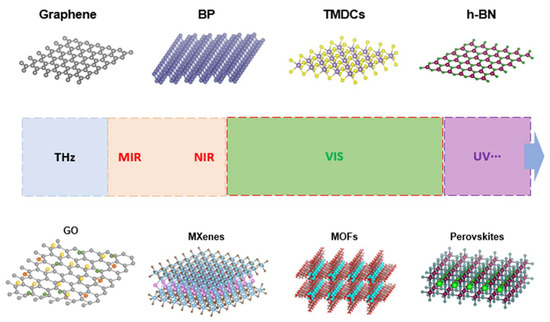
2. 2D Materials
The past decade has witnessed an enormous surge in research on layered 2D materials—many have been discovered and synthesized with a wide range of properties. This section briefly introduce some key 2D materials such as graphene, GO, TMDCs, h-BN, and BP as shown in
Figure 1 and discuss their electrical and optical properties.
Figure 1.
Illustration of typical 2D-layered materials.
2.1. Graphene and Graphene Oxide
Graphene, and its derivative, graphene oxide (GO), have been intensely studied due to their excellent mechanical, electrical, and optical properties
[33][69][70][33,71,72]. Graphene has a gapless band structure, in which the conduction and valence bands meet at the K point of Brillouin zone, resulting in its semimetal nature
[31][44][71][31,44,73]. In contrast, GO is an electronically hybrid material, featuring both conducting
π-states from sp
2 carbon sites and a large energy gap between the σ-states of its sp
3-bonded carbons
[34][72][34,74]. Their unique band structures result in novel electrical and optical properties, where for graphene, for example, the electrons and holes act as massless Dirac fermions resulting in extremely high carrier mobilities (>10
5 cm
2/Vs) even under ambient conditions
[31]. In contrast, GO exhibits a band gap that is tunable by adjusting the degree of reduction, which in turn affects the electric and optical properties. In addition, GO exhibits fluorescence in the near-infrared (NIR), visible and ultraviolet regions
[34][35][36][34,35,36], which is very promising for light emitting devices. Moreover, the excellent nonlinear optical properties of both materials have been reported, including strong saturable absorption (SA)
[73][74][75,76], a giant optical Kerr nonlinearity
[58][59][58,59], leading to efficient self-phase modulation
[75][77], FWM
[76][77][78,79], as well as high harmonic generation
[63].
2.2. Transition Metal Dichalcogenides
Transition metal dichalcogenides (TMDCs) with the formula of MX
2 (where M is a transition metal and X is a chalcogen), is another widely studied family of 2D materials. Different to the semimetal graphene, monolayer TMDCs, such as MoS
2, MoSe
2, WS
2, and WSe
2, are typically semiconductors that have bandgaps from 1 eV to 2.5 eV, covering the spectral range from the near infrared to the visible region
[37][38][37,38]. Moreover, TMDCs can exhibit a transition from direct- to indirect-bandgaps with increasing film thickness, resulting in strongly thickness-tunable optical and electrical properties. For instance, MoS
2 exhibits layer-dependent photoluminescence, with monolayer films showing a much stronger photoluminescence
[78][80]. Monolayer hexagonal TMDCs also exhibit unique band structure valley-dependent properties, such as valley coherence and valley-selective circular dichroism
[37][79][37,81], offering new prospects for novel applications in optical computing and information processing. For the nonlinear optical properties, TMDCs with odd numbers of layers have no inversion symmetry, and so exhibit a non-zero second-order (and higher even-order) nonlinearities that are absent in graphene and even-layer TMDCs
[44][64][44,64]. Recently, noble metal TMDCs, including PdSe
2 and PtSe
2, and PdTe
2, have also attracted increasing interest in the fabrication of high performance electronic and optical devices, such as ultra-broadband photodetectors
[39][40][39,40] as well as mode-locked lasers
[80][82].
2.3. Black Phosphorus
Black phosphorus (BP) is another attractive single element 2D-layered material which has been widely studied. It has a puckered crystal structure, yielding a strong in-plane anisotropy in its physical properties in the “armchair” and “zigzag” directions, opening new avenues for anisotropic electronic and optoelectronic devices
[44][45][81][44,45,83]. Moreover, BP is a semiconductor that features a layer thickness-dependent direct bandgap from 0.3 eV (bulk) to 2.0 eV (monolayer), bridging the gap between the zero-bandgap graphene and large-bandgap TMDCs
[48][81][48,83]. This broad bandgap tunability is very suitable for the photodetection and photonic applications from the visible to mid-infrared spectra regions
[46][47][82][46,47,84]. For the nonlinear optical properties, the layer thickness tunable and polarization-dependent THG and optical Kerr nonlinearity have been demonstrated recently
[81][83][83,85]. Broadband SA has also been observed in BP, demonstrating its strong potential for ultrafast pulsed lasers
[84][85][86][86,87,88].
2.4. Other Emerging 2D Materials
A wide range of other novel 2D low-dimensional materials have been investigated, including h-BN, MXenes, perovskites, as well as MOFs, which greatly enriches the family of 2D materials. h-BN is an electrical insulator with a large bandgap of around 5.9 eV
[41][87][41,89] making h-BN a candidate for ultraviolet light applications. It also has an ultra-flat surface as well as excellent resistance to oxidation and corrosion, which are both highly useful as a dielectric or capping layer to protect the active materials or devices from degradation
[41].
MXenes belong to another family of 2D materials, including 2D transition metal carbides, nitrides, and carbonitrides. Typically, the electronic structure of MXenes can be tuned by varying the surface functional groups. For instance, nonterminated Ti
3C
2 theoretically resembles a typical semimetal with a finite density of states at the Fermi level, whereas it can transition to a semiconductor when terminated with surface groups, such as OH and F groups
[88][90]. MXnens also exhibit superior optical properties, such as a high optical transmittance of visible light (>97% per nm)
[38][89][38,91], and excellent nonlinear optical properties
[57].
Organometal-halide perovskites have a general formula of ABX
3, where typically A = CH
3NH
3+, B = Pb
2+, and X = I
−, Br
−, Cl
− or mixtures
[90][92]. Due to their prominent photovoltaic features and luminescence properties, organometal-halide perovskite semiconductors have been widely used to design high performance solar cells as well as light-emitting diodes
[51][52][53][51,52,53]. Metal-organic frameworks (MOFs) are organic–inorganic hybrid porous crystalline materials with metal ions or metal-oxo clusters coordinated with organic linkers
[91][92][93,94]. Thanks to this unique structure, 2D MOFs exhibit enhanced photo-physical behaviour and are promising for various applications, from light emission and sensing to nonlinear optical applications
[93][94][95,96].