Your browser does not fully support modern features. Please upgrade for a smoother experience.
Submitted Successfully!
 +1 credit
Thank you for your contribution! You can also upload a video entry or images related to this topic.
For video creation, please contact our Academic Video Service.
Video Upload Options
We provide professional Academic Video Service to translate complex research into visually appealing presentations. Would you like to try it?
Cite
If you have any further questions, please contact Encyclopedia Editorial Office.
Chen, Z.; Wang, Z.; Wang, J.; Chen, S.; Zhang, B.; Li, Y.; Yuan, L.; Duan, Y. Graphene Based TE Materials. Encyclopedia. Available online: https://encyclopedia.pub/entry/40788 (accessed on 24 June 2026).
Chen Z, Wang Z, Wang J, Chen S, Zhang B, Li Y, et al. Graphene Based TE Materials. Encyclopedia. Available at: https://encyclopedia.pub/entry/40788. Accessed June 24, 2026.
Chen, Ziqiang, Zhenyu Wang, Jintao Wang, Shuming Chen, Buyue Zhang, Ye Li, Long Yuan, Yu Duan. "Graphene Based TE Materials" Encyclopedia, https://encyclopedia.pub/entry/40788 (accessed June 24, 2026).
Chen, Z., Wang, Z., Wang, J., Chen, S., Zhang, B., Li, Y., Yuan, L., & Duan, Y. (2023, February 03). Graphene Based TE Materials. In Encyclopedia. https://encyclopedia.pub/entry/40788
Chen, Ziqiang, et al. "Graphene Based TE Materials." Encyclopedia. Web. 03 February, 2023.
Copy Citation
Graphene is a two-dimensional (2D) monolayer material with only one carbon atom thickness. The most promising method for transparent conductive graphene electrodes in optoelectronic devices is reportedly synthesized via chemical vapor deposition, where graphene films are deposited directly on a substrate such as Cu foil by passing a carbon source through a high-temperature vacuum chamber, and the synthesized graphene is transferred to the target substrate using a support film such as poly (methyl methacrylate).
transparent electrodes
organic optoelectronic devices
graphene
1. Modification and Doping of Graphene
Graphene monolayer is not inherently a highly conductive electrode material, because its defects Rs is about 1000 Ω/sq, and the lowest figure of merit (FOM) in the photovoltaic field up to date [1]. As shown in Figure 1a, ideal graphene provides a flawless transport pathway for electrons or holes, avoids the concern of high resistance losses when applied in organic optoelectronic devices. However, graphene monolayer is often produced with defects in the preparation process, as shown in Figure 1b, graphene with defects affects its conductive properties as TE materials, there is a natural effect on the electronic structure, which leads to electron or hole transport is hampered and reduces the lateral conductivity of graphene, and results in low carrier concentration and a large potential energy barrier [2]. Graphene and any other 2-d materials has a very low transmittance and is also a major reason why it’s used in conjugation with other materials and not standalone. Therefore, the modification and stable doping of graphene are extremely important to obtain graphene composite TEs with Rs below 100 Ω/sq and above 90% optical transmittance.
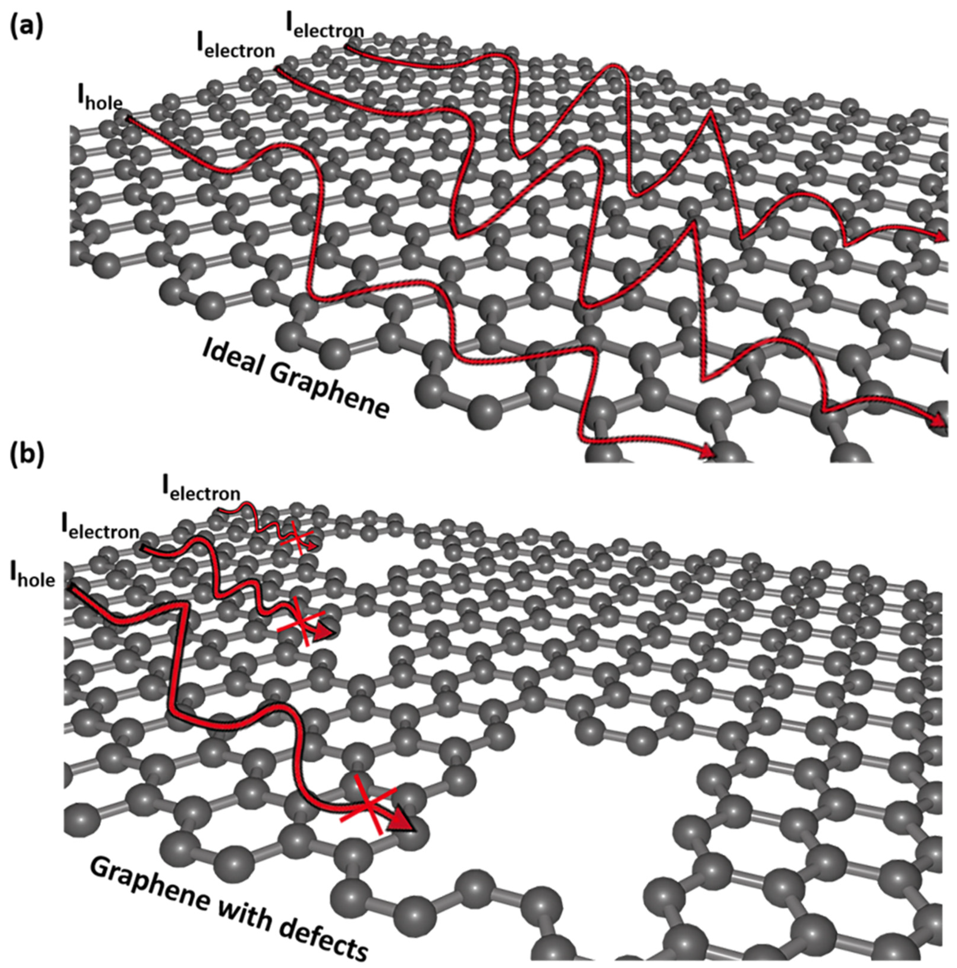
Figure 1. The schematic illustration of electron or hole transport path in: (a) ideal graphene provides a flawless transport pathway for electrons or holes, while it is hampered in (b) defective graphene.
2. Reduced Graphene Oxide
A common modification method for graphene is reduced graphene oxide (RGO), a low-cost method compatible with roll-to-roll (R2R) mass production, where graphene oxide (GO) is chemically peeled by ultrasonic dispersion or rapid thermal expansion, and then reduced by appropriate chemical or laser-assisted methods [3]. RGO can be easily produced in large volumes as graphene ink by taking advantage of its better solubility in common solutions [4]. Based on this situation, RGO TEs have been extensively researched. Without sacrificing the optical transmittance, RGO cannot effectively reduce the resistance and roughness of the bottom layer, therefore, similar to graphene monolayer, RGO also need combine together with other electrode materials [5][6][7].
3. Composite Preparation of Graphene Transparent Electrodes
The conductivity of graphene monolayer is poor, in order to meet the application of graphene TEs in optoelectronic devices, as shown in Figure 2, graphene monolayer is usually combined together with metal oxide, CNT, MNWs and metal thin film [8][9][10][11].
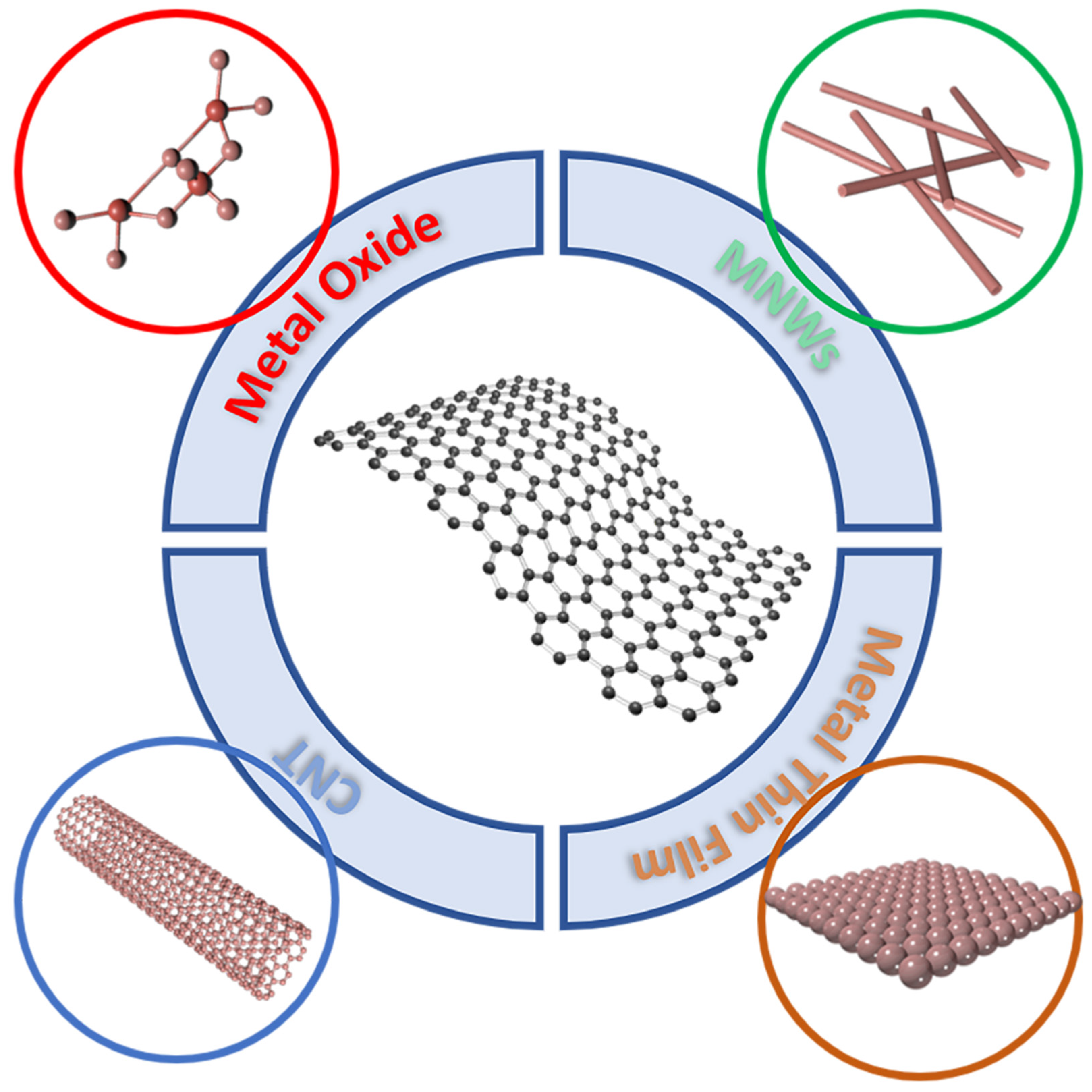
Figure 2. The schematic illustration of graphene composite preparation with typical nanomaterials. Such as metal oxide, MNWs, CNT and metal thin film, resolved the poor lateral conductivity of graphene monolayer.
CNT films have excellent chemical stability and conductivity. However, the adhesion to the substrate is weak, and its unique tube-tube junction can easily open causing a rise in Rs, so CNT is often hybrid with other electrode materials such as graphene to prepare electrodes. On the basis of this, Geng et al. performed polydopamine (PDA) functionalized of the RGO as plotted in Figure 3a, and thus combined with single-walled CNT (SWCNT) [12]. As illustrated in Figure 3b,c, PDA-RGO/SWCNT/poly(3,4-ethylenedioxythiophene) polystyrene sulfonate (PEDOT:PSS) composite TEs with a structure similar to that of reinforced concrete were fabricated. This structure has excellent mechanical stability during bending, and the PDA-RGO improves the adhesion of the conductive layer with the substrate. The conductivity of the composite electrode is significantly improved, with a sheet resistance of 52.2 Ω/sq and an optical transmission of 88.7% at 550 nm. The composite TE has the potential as an organic light-emitting diode (OLED) anode, and the prepared device has a luminance of 2032 cd/cm2 at 15 V and maximum current efficiency of 2.13 cd/A at 14 V.
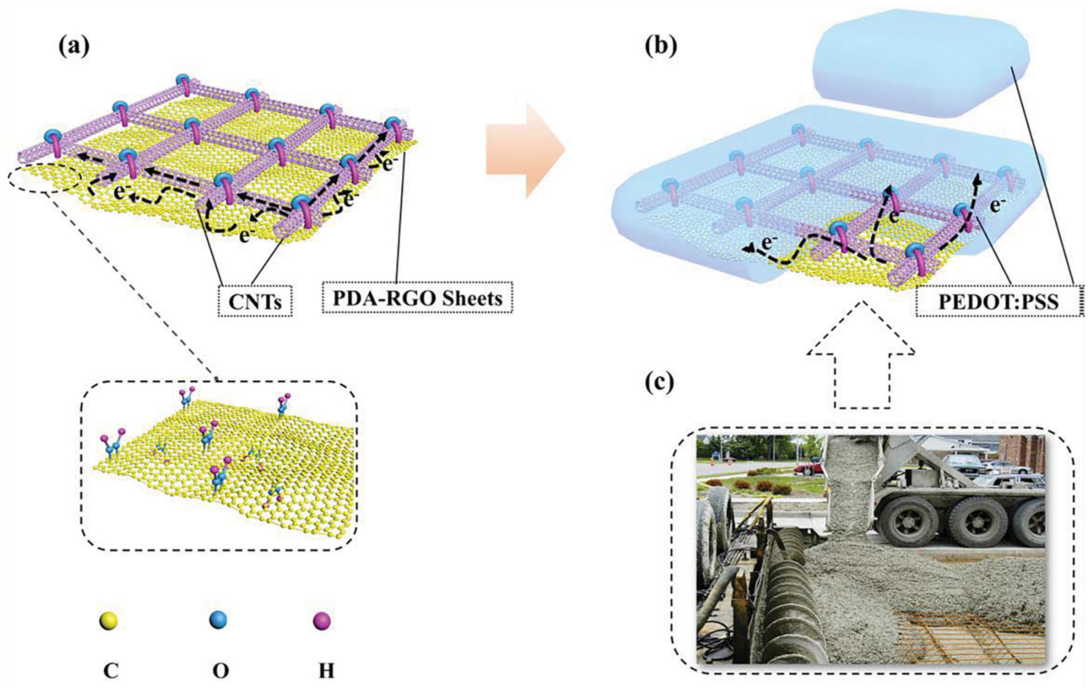
Figure 3. The schematic illustration of TCFs with ultra-adhesion, relatively low roughness, and excellent electrical conductivity: (a) PDA−RGO/CNT and (b) PDA−RGO/CNT/PEDOT:PSS. (c) A picture of reinforced concrete structure used in building construction. (Reproduced from [12] with permission from Elsevier, 2020).
In the previous work, researchers provided a graphene optimization method, researchers prepared Au-doped graphene films, and through improving the concentration of dopant solution (AuCl3) and doping time, researchers prepared flexible transparent graphene electrode with Rs reduced from 365 Ω/sq to 90 Ω/sq, and 85.6% transmittance at 550 nm. When applied in OLED device, it exhibited higher performance both in terms of illumination and device efficiency [13]. MNWs are widely applied as TE materials [14]. The distribution of MNWs is random and the conductivity is severely affected by boundary effects, which arise from the fact that the atoms on the surface of MNWs that are not fully bonded as those of the monolithic material, which makes the electrical conductivity of MNWs lower than that of the monolithic material [15][16]. As the size of MNWs decreases, the number of surface atoms increases relative to the number of monolithic atoms, and thus the boundary effects become more pronounced [17]. Good electrical conductivity requires upgrading the length of MNWs. However, micron-scale lengths can make the prepared films have significant protrusions, so MNWs are often hybrid with other electrode materials such as graphene to prepare electrodes.
Accordingly, Grossman et al. reported a highly stable electrophoretic deposition (EPD)-GO/silver nanowires (AgNWs)/GO TE, which has a similar sandwich structure fabricated by utilizing the EPD method for GO, where AgNWs serve as a conductive bridge covered by GO films on both sides [18]. This newly developed all-solution process allowed transparent conductive films to be transferred to alternate surfaces after deposition and demonstrates excellent Rs (15 Ω/sq). In addition, simply changing the thickness of EPD-GO, its transmittance can be adjusted from 70% and 87% at 550 nm. In contrast with bare AgNWs, the composite electrode retains its original conductivity over long periods of operation at 80% relative humidity. the AgNWs networks are effectively “interposed” between the two layers of GO providing combined stability and performance.
In a research work published by Berry’s research team, it was demonstrated that ideally flawless graphene can be utilized as a multifunctional encapsulating layer, because the gaps within the aromatic rings of carbon are nearly zero due to the overlapping electron clouds, preventing the penetration of gas molecules, even tiny helium molecules [19].
Accordingly, Grossman et al. utilized ultrathin GO as an encapsulation layer to protect the AgNWs from the PEDOT:PSS-hole transport layer (HTL), thus not affecting the energy level alignment of the device [20]. EPD-GO/AgNWs/GO as an organic solar cell (OSC) anode to substantially improve the lifetime of inverted translucent OSC, without additional encapsulation, the lifetime of the entire device is increased by a factor of five.
4. ALD-Oxide on Graphene
ALD-oxide (Atomic Layer Depostion-oxide) is an essential material for the perovskite solar cell (PSC) electron transport layer, organic optoelectronic device encapsulation layer, and TEs dielectric layer. However, due to the surface structure of graphene and the step-covering deposition of ALD, ALD oxides are difficult to deposit on graphene, so it is a challenging task to utilize graphene and ALD-oxide simultaneously [21][22][23][24]. Accordingly, as shown in Figure 4, people usually deposited a functional layer before depositing the ALD-oxide on the graphene, which can be a useful aid to the deposition of the ALD-oxide [25]. Herein, researchers utilized ethylene glycol (EG) as a precursor to prepare a functional layer to activate the graphene surface and thus improve the deposition of ALD-ZnO films [26]. The prepared EG-Graphene/ALD-ZnO composite films exhibit a significant reduction in Rs, higher transmittance, smooth and uniform surface, excellent bending ability and energy level matching with other device components. Lee et al. utilized NO2 to provide nucleation sites for the deposition of ALD-Al2O3 on graphene to increase surface reactivity, promoting in the deposition of uniform Al2O3 layers on graphene [27].
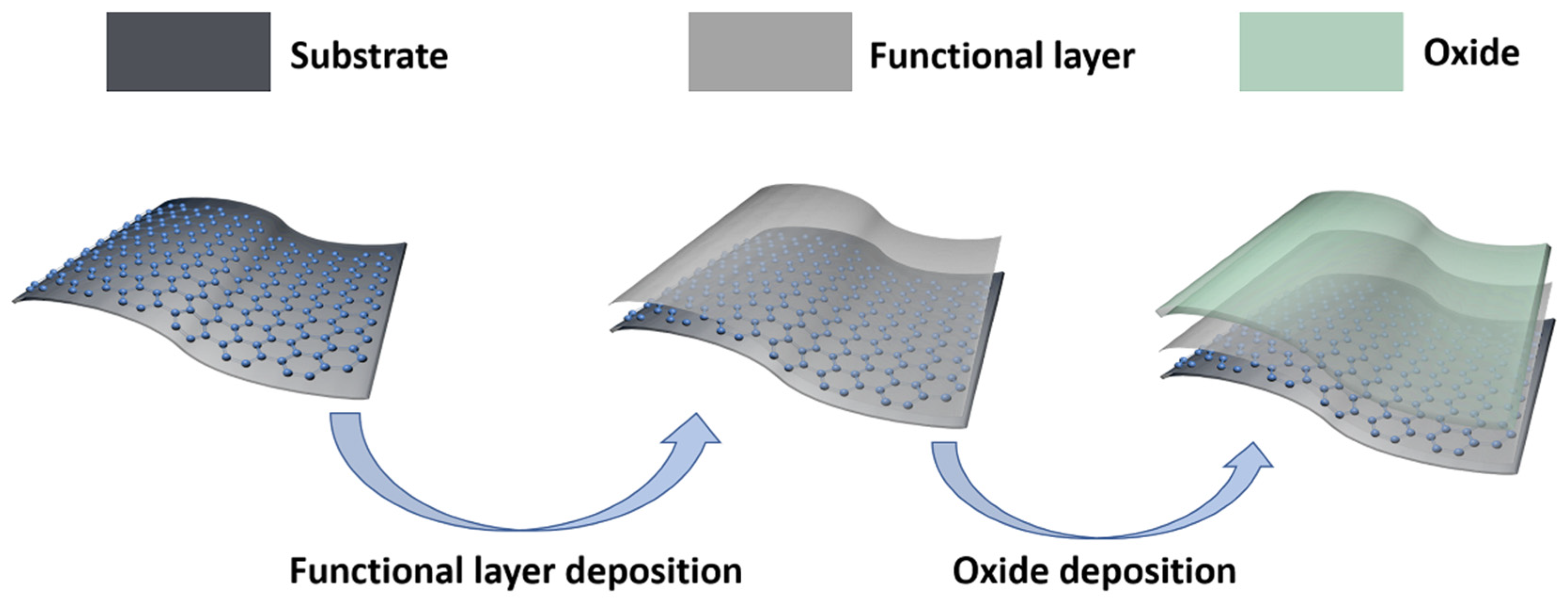
Figure 4. The solution for the deposition of oxides on flexible graphene substrate. The schematics, respectively, illustrate the flexible substrate with graphene, the deposition of a functional layer on graphene, and the fact that the oxide can be deposited well after the deposition of the functional layer.
5. Other Methods
Contrary to doping and modification, graphene monolayer can also be prepared without composite with other conductive materials. For instance, adhesion enhancement between the graphene monolayer and substrate compensates the defects of the graphene monolayer by graphene multilayer.
Graphene monolayer has poor adhesion to the substrate, and the graphene surface is easily contaminated by dust during the process of peeling off from the metal foil or transferring to the target substrate. These challenges make it difficult to utilize in industrial production. Koo et al. combined graphene film directly with polyimide (PI) to obtain TEs with high flexibility and thermal stability [28]. As plotted in Figure 5, the PI containing dual functionalities on CVD-grown graphene, which acts as both a carrier film and a substrate for the graphene electrode, exhibits an ultra-clean surface, along with an optical transmittance of over 92%, a sheet resistance of 83 Ω/sq. In addition, the direct integration of PI improves the durability of the graphene electrode by reducing the mechanical exfoliation process of the graphene. The power conversion efficiency (PCE) of OSC has obtained significant progress of 15.2%.
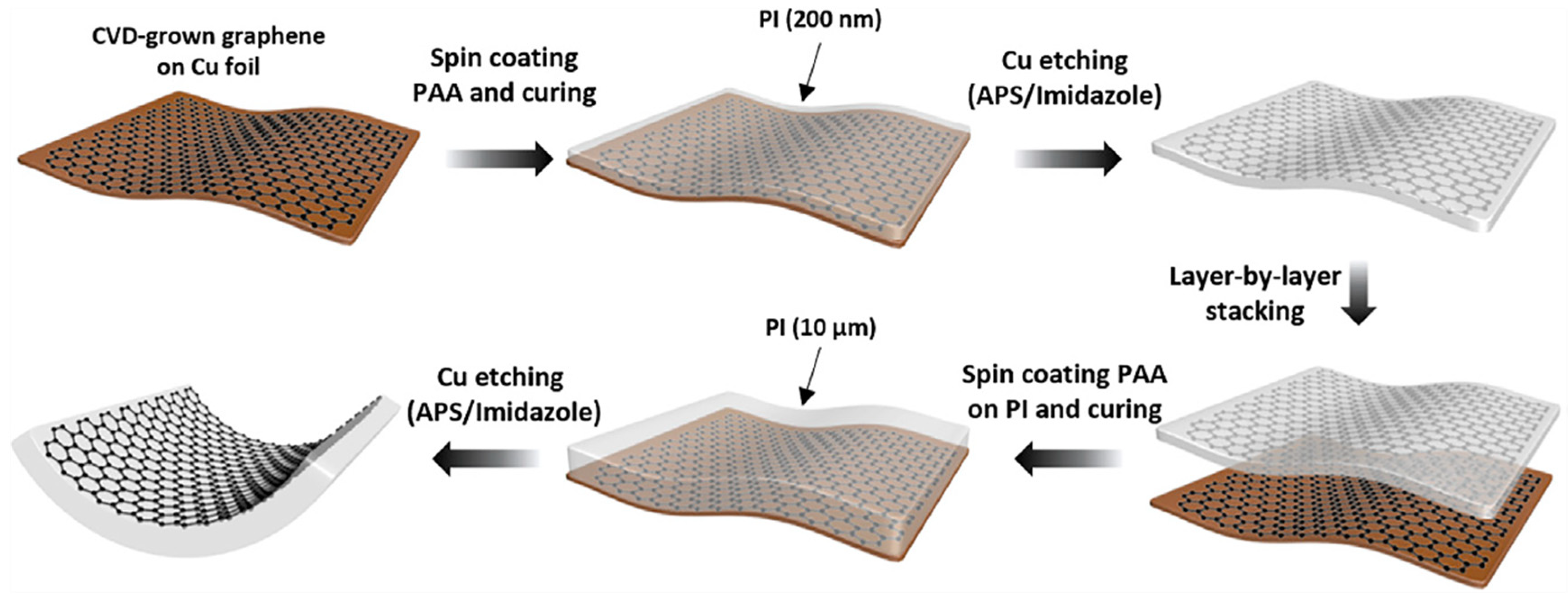
Figure 5. 200-nm-thin PI and 10-mm-thick PI were applied as a carrier film during graphene transfer and a substrate for the graphene electrode, respectively (Reproduced from [28]with permission from Elsevier, 2020).
The photovoltaic properties of graphene multilayer, as compared to graphene monolayer, have also been extensively researched. However, contrary to the main theme of this review, therefore, it will not be described in detail.
References
- Haacke, G. New figure of merit for transparent conductors. J. Appl. Phys. 1976, 47, 4086–4089.
- Banhart, F.; Kotakoski, J.; Krasheninnikov, A.V. Structural defects in graphene. ACS Nano 2011, 5, 26–41.
- Hwang, B.; Park, M.; Kim, T.; Han, S.M. Effect of RGO deposition on chemical and mechanical reliability of Ag nanowire flexible transparent electrode. RSC Adv. 2016, 6, 67389–67395.
- Tarcan, R.; Todor-Boer, O.; Petrovai, I.; Leordean, C.; Astilean, S.; Botiz, I. Reduced graphene oxide today. J. Mater. Chem. C 2020, 8, 1198–1224.
- Fernández-Merino, M.J.; Guardia, L.; Paredes, J.; Villar-Rodil, S.; Solís-Fernández, P.; Martínez-Alonso, A.; Tascón, J. Vitamin C is an ideal substitute for hydrazine in the reduction of graphene oxide suspensions. J. Phys. Chem. C 2010, 114, 6426–6432.
- Shin, H.J.; Kim, K.K.; Benayad, A.; Yoon, S.M.; Park, H.K.; Jung, I.S.; Jin, M.H.; Jeong, H.K.; Kim, J.M.; Choi, J.Y. Efficient Reduction of Graphite Oxide by Sodium Borohydride and Its Effect on Electrical Conductance. Adv. Funct. Mater. 2009, 19, 1987–1992.
- Moon, I.K.; Lee, J.; Ruoff, R.S.; Lee, H. Reduced graphene oxide by chemical graphitization. Nat. Commun 2010, 1, 73.
- Kim, K.; Lee, H.-B.-R.; Johnson, R.W.; Tanskanen, J.T.; Liu, N.; Kim, M.-G.; Pang, C.; Ahn, C.; Bent, S.F.; Bao, Z. Selective metal deposition at graphene line defects by atomic layer deposition. Nat. Commun 2014, 5, 1–9.
- Xu, X.; Liu, Z.; He, P.; Yang, J. Screen printed silver nanowire and graphene oxide hybrid transparent electrodes for long-term electrocardiography monitoring. J. Phys. D: Appl. Phys. 2019, 52, 455401.
- Han, J.T.; Kim, J.S.; Jo, S.B.; Kim, S.H.; Kim, J.S.; Kang, B.; Jeong, H.J.; Jeong, S.Y.; Lee, G.-W.; Cho, K. Graphene oxide as a multi-functional p-dopant of transparent single-walled carbon nanotube films for optoelectronic devices. Nanoscale 2012, 4, 7735–7742.
- Meyer, J.; Kidambi, P.R.; Bayer, B.C.; Weijtens, C.; Kuhn, A.; Centeno, A.; Pesquera, A.; Zurutuza, A.; Robertson, J.; Hofmann, S. Metal oxide induced charge transfer doping and band alignment of graphene electrodes for efficient organic light emitting diodes. Sci. Rep. 2014, 4, 5380.
- Wang, T.; Jing, L.-C.; Zhu, Q.; Ethiraj, A.S.; Tian, Y.; Zhao, H.; Yuan, X.-T.; Wen, J.-G.; Li, L.-K.; Geng, H.-Z. Fabrication of architectural structured polydopamine-functionalized reduced graphene oxide/carbon nanotube/PEDOT:PSS nanocomposites as flexible transparent electrodes for OLEDs. Appl. Surf. Sci. 2020, 500, 143997.
- Wei, M.; Wang, H.; Wang, J.; Chen, P.; Zhao, W.; Chen, X.; Guo, J.; Kang, B.; Duan, Y. Flexible transparent electrodes for organic light-emitting diodes simply fabricated with AuCl3-modied graphene. Org. Electron. 2018, 63, 71–77.
- Lee, M.-S.; Kim, J.; Park, J. Studies on the mechanical stretchability of transparent conductive film based on graphene-metal nanowire structures. Nanoscale Res. Lett. 2015, 10, 27.
- Sannicolo, T.; Lagrange, M.; Cabos, A.; Celle, C.; Simonato, J.P.; Bellet, D. Metallic nanowire-based transparent electrodes for next generation flexible devices: A review. Small 2016, 12, 6052–6075.
- Patil, J.J.; Chae, W.H.; Trebach, A.; Carter, K.J.; Lee, E.; Sannicolo, T.; Grossman, J.C. Failing forward: Stability of transparent electrodes based on metal nanowire networks. Adv. Mater. 2021, 33, 2004356.
- Hecht, D.S.; Hu, L.; Irvin, G. Emerging transparent electrodes based on thin films of carbon nanotubes, graphene, and metallic nanostructures. Adv. Mater. 2011, 23, 1482–1513.
- Chae, W.H.; Sannicolo, T.; Grossman, J.C. Double-Sided Graphene Oxide Encapsulated Silver Nanowire Transparent Electrode with Improved Chemical and Electrical Stability. ACS Appl Mater Interfaces 2020, 12, 17909–17920.
- Berry, V. Impermeability of graphene and its applications. Carbon 2013, 62, 1–10.
- Sannicolo, T.; Chae, W.H.; Mwaura, J.; Bulović, V.; Grossman, J.C. Silver Nanowire Back Electrode Stabilized with Graphene Oxide Encapsulation for Inverted Semitransparent Organic Solar Cells with Longer Lifetime. ACS Appl. Energy Mater. 2021, 4, 1431–1441.
- Kim, M.J.; Alvarez, S.; Chen, Z.; Fichthorn, K.A.; Wiley, B.J. Single-crystal electrochemistry reveals why metal nanowires grow. J. Am. Chem. Soc. 2018, 140, 14740–14746.
- Zhao, W.; Duan, Y. Advanced Applications of Atomic Layer Deposition in Perovskite-Based Solar Cells. Adv. Photonics Res. 2021, 2, 2100011.
- Seo, S.; Park, I.J.; Kim, M.; Lee, S.; Bae, C.; Jung, H.S.; Park, N.-G.; Kim, J.Y.; Shin, H. An ultra-thin, un-doped NiO hole transporting layer of highly efficient (16.4%) organic–inorganic hybrid perovskite solar cells. Nanoscale 2016, 8, 11403–11412.
- Zhou, Y.; Wang, J.; He, P.; Chen, S.; Chen, Z.; Zang, Y.; Li, Y.; Duan, Y. ALD-Assisted Graphene Functionalization for Advanced Applications. J. Electron. Mater. 2022, 51, 2766–2785.
- Hendricks, O.L.; Tang-Kong, R.; Babadi, A.S.; McIntyre, P.C.; Chidsey, C.E. Atomic Layer Deposited TiO2–IrO x Alloys Enable Corrosion Resistant Water Oxidation on Silicon at High Photovoltage. Chem. Mater. 2018, 31, 90–100.
- Xu, X.; Wang, H.; Wang, J.; Muhammad, M.; Wang, Z.; Chen, P.; Zhao, W.; Kang, B.; Zhang, J.; Li, C. Surface Functionalization of a Graphene Cathode to Facilitate ALD Growth of an Electron Transport Layer and Realize High-Performance Flexible Perovskite Solar Cells. ACS Appl. Energy Mater. 2020, 3, 4208–4216.
- Nam, T.; Park, Y.J.; Lee, H.; Oh, I.-K.; Ahn, J.-H.; Cho, S.M.; Kim, H. A composite layer of atomic-layer-deposited Al2O3 and graphene for flexible moisture barrier. Carbon 2017, 116, 553–561.
- Koo, D.; Jung, S.; Seo, J.; Jeong, G.; Choi, Y.; Lee, J.; Lee, S.M.; Cho, Y.; Jeong, M.; Lee, J. Flexible Organic Solar Cells Over 15% Efficiency with Polyimide-Integrated Graphene Electrodes. Joule 2020, 4, 1021–1034.
More
Information
Subjects:
Physics, Applied
Contributors
MDPI registered users' name will be linked to their SciProfiles pages. To register with us, please refer to https://encyclopedia.pub/register
:
View Times:
1.1K
Revisions:
3 times
(View History)
Update Date:
14 Feb 2023
Table of Contents


Notice
You are not a member of the advisory board for this topic. If you want to update advisory board member profile, please contact office@encyclopedia.pub.
OK
Confirm
Only members of the Encyclopedia advisory board for this topic are allowed to note entries. Would you like to become an advisory board member of the Encyclopedia?
Yes
No
${ textCharacter }/${ maxCharacter }
Submit
Cancel
Back
Comments
${ item }
|
${ item.createdUser.fullName }
${ item.createdAt }
${ item.vote }
${ item.reply }
Delete
${ reply.createdUser.fullName }
${ reply.createdAt }
${ reply.vote }
Delete
There is no reply to this comment~
${ item.replyTextCharacter }/${ item.replyMaxCharacter }
Submit
Cancel
More
No more~
There is no comment~
${ textCharacter }/${ maxCharacter }
Submit
Cancel
${ selectedItem.replyTextCharacter }/${ selectedItem.replyMaxCharacter }
Submit
Cancel
Confirm
Are you sure to Delete?
Yes
No