 +1 credit
| Version | Summary | Created by | Modification | Content Size | Created at | Operation |
|---|---|---|---|---|---|---|
| 1 | Lado Filipovic | -- | 6224 | 2022-11-24 09:49:24 | | | |
| 2 | Lindsay Dong | + 108 word(s) | 6332 | 2022-11-28 11:57:29 | | | | |
| 3 | Lindsay Dong | -33 word(s) | 6299 | 2022-12-01 12:19:06 | | | | |
| 4 | Lado Filipovic | -13 word(s) | 6286 | 2022-12-01 15:53:46 | | | | |
| 5 | Lindsay Dong | Meta information modification | 6286 | 2022-12-02 09:41:38 | | |
Video Upload Options
The semiconductor metal oxide (SMO)-based gas sensor, considered the current workhorse of semiconductor-based chemiresistive gas sensor technologies, requires high temperatures to initiate the surface reactions which result in the sensing response, making it difficult to fabricate and prone to high mechanical instability. Therefore, alternatives at lower temperatures are desired, where 2D materials seem to hold the most promise. Even at ambient temperature, their sensitivity is extraordinarily large due to their extremely high surface-to-volume ratio. However, some ongoing issues still need to be resolved before gas sensors based on 2D materials can be widely used and commercialized. The alternative room temperature solutions involve optical signals, either by designing an nondispersive infrared (NDIR) sensor based on the Beer-Lambert law or by introducing an additional UV illumination to SMO sensors. In both cases, complementary metal oxide semiconductor (CMOS) integration is not feasible, which is why continued interest in 2D-material-based gas sensors persists.
1. Gas Sensing Technologies
A large set of materials for gas sensing and gas sensor designs are under investigation and find themselves at vastly different maturity levels of realizable development. Several advanced gas sensing technologies which have already been commercialized by industry include electrochemical (EC) sensors, catalytic pellistors (CP), thermal pellistors (TP), piezo-electric (PE) sensors, photo-ionization (PI) devices, optical infrared (IR) adsorption sensors, and semiconductor metal oxide (SMO) chemiresistors [1][2][3][4]. These technologies are typically divided into two categories: One whose detection mechanism is based on changing a material’s electrical behavior after adsorption (e.g., conductivity, field effect) and a second whose detection depends on an induced change in another property (e.g., thermal, optical) [5].
The semiconductor-based chemiresistive technology provides an option with the lowest cost, footprint, and power dissipation, mainly as a consequence of its successful integration with complementary metal oxide semiconductor (CMOS) fabrication techniques. These characteristics are necessary in order to enable sensing solutions for portable technologies as well as IoE and IoT integration, while integration with CMOS further ensures a means for very high and reliable reproducibility [6]. It is crucial for the volume manufacturing of commercial devices that there be minimal inter-device variances and that there is high confidence in the capability to produce a device with predictable attributes and highly manageable tolerances. It also observes a low power dissipation attributed to the catalytic pellistor which is also inexpensive to manufacture and has a comparatively small physical footprint. However, compared to the semiconductor metal oxide (SMO) sensor, this device has far worse selectivity, lesser sensitivity, and a slower reaction time. Piezoelectric, photo-ionization, and infrared sensors all offer excellent sensitivity, but they all have the drawback of high power consumption, which prevents portability and internet-of-things (IoT) integration.
In comparison to existing alternatives, the SMO sensor appears to provide the most benefits towards potential IoT applications. Previous research has shown that it has several advantages leading to its commercialization [7][8][9][10][11][12][13][14], particularly in terms of response time, sensitivity, and possibilities for portability and down-scaling. The high sensitivity of SMO sensors is, however, only made possible by applying very high operating temperatures, which may compromise their reliability and durability. With the goal of CMOS integration for a chemiresistive gas sensing solution, the SMO sensor has emerged as the industry standard. A semiconductor-based approach, which operates at ambient temperature and can be designed with established CMOS fabrication techniques is, therefore, highly desired. Several sensors and prospective sensing materials, including two-dimensional (2D) semiconductors such as graphene and transition metal dichalcogenides (TMDs), are being investigated in this direction [15]. The fabrication of these films, and devices based on these films, is not trivial. Nevertheless, investigations in the past few years have shown some promise in fabricating films of high quality for sensing and have made significant progress [16][17].
2. Semiconductor-Based Gas Sensor Types
2.1. Chemiresistors
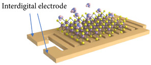
For chemiresistors, the electrical resistance of the sensor changes as a consequence of the adsorption of gas molecules on its surface. The sensitivity S towards a particular gas is, therefore, determined by how much the resistance of the film changes after exposure to this gas, usually starting from a baseline using operating conditions in pure ambient air. However, it should be noted that some studies use inert ambient, e.g., N2, as the baseline resistance, which is why it is often difficult to truly compare sensitivities across a broad set of experimental literature studies. From all of the available types of semiconductor-based gas sensors, the chemiresistor is the easiest to fabricate, since it only requires placing the sensing film on top of an insulating substrate and adding two metal contacts, which are often formed using interdigitated electrodes, as shown in Figure 1. The read-out circuit for the chemiresistive gas sensor is also quite straight-forward since only the current flowing through the resistor needs to be measured, which can be performed by placing a load resistor and reading the voltage across it [19][20]. The ease of chemiresistive gas sensor fabrication brings about the potential for their cost-efficient fabrication, ability of scaling, and eventual CMOS integration.
2.2. Field Effect Transistors
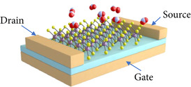
The field-effect transistor (FET) is the workhorse of the semiconductor industry and is the cornerstone of digital logic and many memory devices. In addition, the field effect, as implemented in a FET or a metal-oxide-semiconductor FET (MOSFET), has been extensively used in advanced bio-sensing technologies with the biologically sensitive field-effect transistor (BioFET) [25][26] and ion-sensitive field-effect transistor (ISFET) [27][28] designs. These devices provide a means to adjust the electrostatics of the channel layer using an electrode, which is suspended in an electrolyte solution, which is in contact with the gate dielectric. The sensitivity of the BioFET and ISFET structures are governed by how the charge accumulation changes on the gate dielectric and the selectivity is introduced by placing immobilized receptors on top the gate, which will only react to specific bio-molecules. However, generating such a structure, which has a high sensitivity and selectivity, for gas sensing is more challenging. In bio-sensors and BioFETs the electrolyte serves to keep undesired molecules out of the gate or channel regions. For gas sensors, on the other hand, exposing the channel to the ambient means it is exposed to any molecule which may come in its vicinity, shown in Figure 2.
3. Fabrication and Working Principle of 2D-Material-Based Gas Sensors
The semiconductor industry is clearly dominated by silicon, and the introduction of new applications and technologies on silicon is usually a stepping stone towards mass production and adoption in the market. Over the years, many materials have attempted to replace silicon, including materials with higher charge carrier mobility, such as germanium, and various group III-IV materials. However, none have been successful in commercialization on a broad scale and have only made breakthroughs in certain niche markets [43]. The continued scaling of silicon appears to have reached saturation and sub-3 nm channels pose significant challenges due to increased variability and reliability issues, but also due to the limited carrier mobility at these reduced scales [44][45].
Beyond transistor scaling and digital logic, interest in 2D materials has intensified over the past years due to their potential usability in a wide range of applications. Due to the low dimensionality of these materials, they exhibit properties of relevance to several research fields from solid-state physics to low dimensional molecular chemistry. Therefore, even minor shifts in the chemical structure of the film’s surface can be felt in its bulk properties. This feature makes 2D materials ideal for catalysis [46][47][48][49] and sensing [50][51][52]. The range of application for gas sensing is immense and includes devices which are able to detect hazardous gases, organic vapors, and humidity: Devices frequently used for medical diagnostics, environmental monitoring, and safety and security [52]. TMDs including MoS2, MoTe2, WSe2, and SnS2 have already been widely studied for gas sensing in the FET configuration, primarily for the detection of nitrogen-containing compounds. In the chemiresistor configuration, a broader group of 2D materials have shown high potential for gas sensor development, including TMDs, boron nitride, black phosphorus, and MXenes [30][53].
3.1. Synthesis of 2D Materials
A thorough review of the means by which 2D materials are synthesized is provided by Knobloch in [54]. Here, these processes are viewed from the perspective of CMOS integration. The initial discovery of 2D materials for electronic applications was enabled by the mechanical exfoliation of single or few layers of graphene from a layered bulk crystal graphite [55]. While this process is not scalable and does not lend itself to CMOS integration, it is still frequently used in lab-based research into 2D materials and devices due to the simplicity of the process and the reasonable quality of films which can be achieved. The process involves thinning down a thick layer of a 2D crystal by placing it on adhesive tape. Subsequently, by frequently folding and unfolding the tape, increasingly fewer layers remain. These layers are then transferred to a wafer, typically SiO2-on-silicon [54][56][57].
3.1.1. Chemical Vapor Deposition
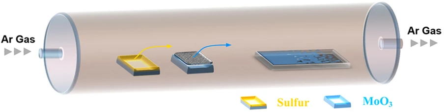
Chemical vapor deposition (CVD) is probably the most widely studied means of depositing a film and is a staple of the microelectronics industry and of a CMOS foundry. It is a relatively simple bottom-up growth process which offers flexibility of metal precursor and a relatively fast growth rate. Several studies have examined the growth of graphene, hexagonal Boron Nitride (hBN), and TMDs using CVD, while only a few studies have looked into growing black phosphorene with this method. This has to do with black phosphorus’ tendency to quickly oxidize in the presence of oxygen, requiring an oxygen-free growth environment. Furthermore, a precursor is required to grow the material. For MoS2, the precursor is the chalgogen sulfur, as shown in Figure 3 for phosphorene, this would be phosphine, which is a highly toxic material [59].
3.1.2. Physical Vapor Deposition
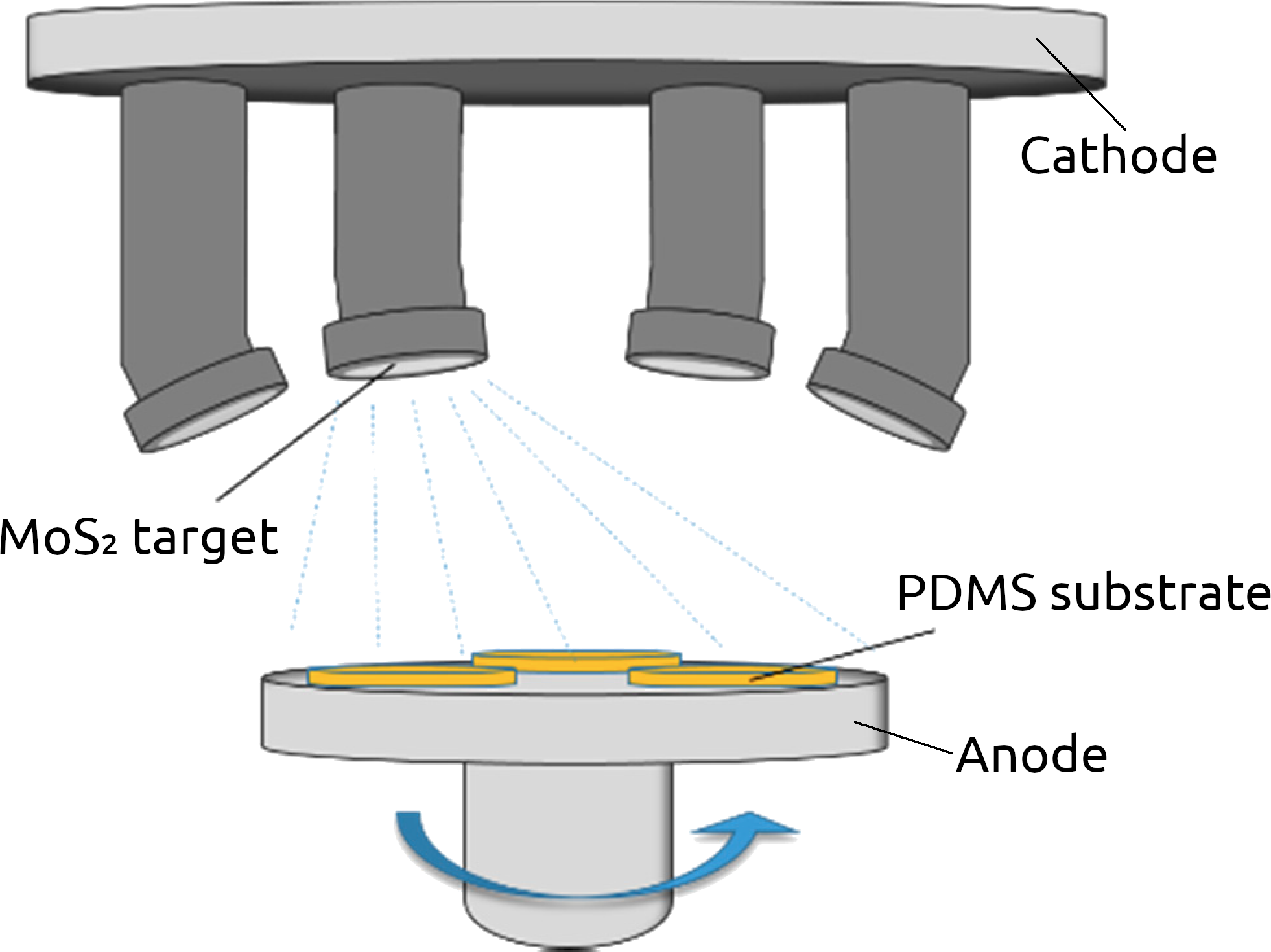
A typical alternative to CVD in a CMOS foundry is physical vapor deposition (PVD) which most often refers to thermal evaporation deposition or sputtering. PVD belongs to a family of synthesis processes which enable large-scale processing of 2D van der Waals (vdW) materials. Figure 4 shows such a setup for the sputtering of MoS2 films from a target. There is no fundamental limit on the size or shape of the films which can be generated using this process, which has been used to produce thicker vdW films for decades [65][66], while the deposition of a few layers has also been recently demonstrated [67][68]. PVD also does not require the transfer of the grown material onto the desired substrate, as growth on any substrate is inherently possible.
3.1.3. Molecular-Beam Epitaxy
Molecular-beam epitaxy (MBE) is a process by which epitaxial growth can be performed on a large scale in an ultra-high vacuum chamber with pressures in the sub 10−10 mbar range [72] and a typical MBE setup is shown in Figure 5. In MBE, the precursor molecules form a film on a heated crystalline substrate, which only provides the crystallographic information for the formation of the new film [54]. Since the substrate does not provide any catalytic surface effects, MBE results in a direct in situ growth of vertically-stacked heterostructures [73].
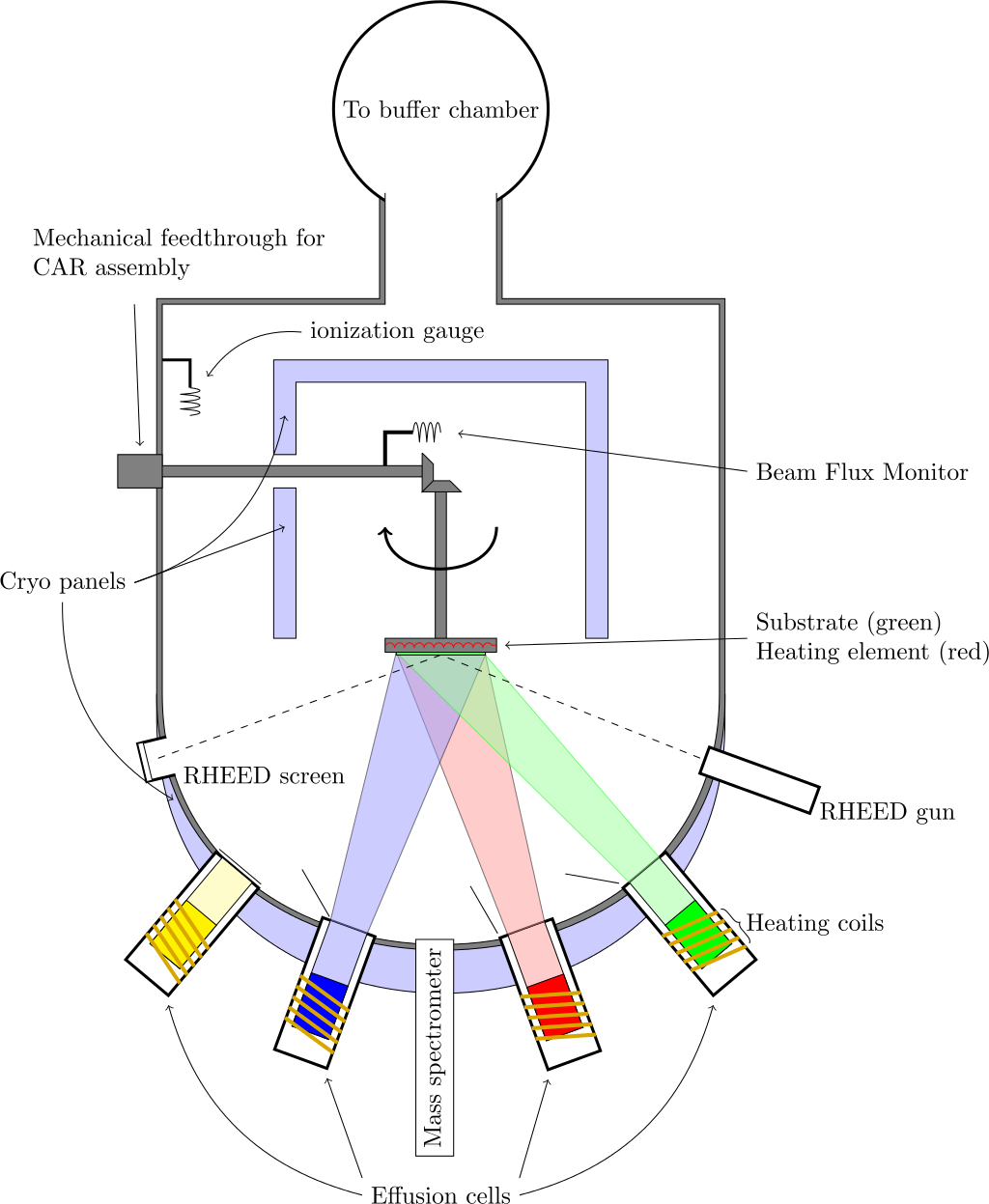
Figure 5. Schematic of the MBE setup. (Reprinted from Vegar Ottesen, CC BY 3.0, via Wikimedia Commons)
MBE is a very powerful tool for growing high-quality crystalline 2D films and has been extensively used to realize many films, including graphene, TMDs, and elemental 2D materials [74]. In addition, MBE has been applied to grow vertical and lateral vdW heterostructures [75]. There are, however, several difficulties in integrating MBE within a CMOS technology flow. The high vacuum requirements and high process sensitivity to small variations are a particular concern for mass production. Therefore, the technology remains principally a research tool for studying the fundamental properties of various material systems [76].
3.1.4. Atomic Layer Deposition
Atomic layer deposition (ALD) is a method of thin film deposition which offers more control over film conformality and thickness than traditional CVD. A typical multi-step ALD flow is shown in Figure 6. Because it may be used to deposit technologically important oxides and nitrides, such as the gate oxide HfO2 and gate metal TiN, ALD has emerged as a fundamental technique in semiconductor processing for advanced nodes. This is primarily due to the self-limiting nature of the process. In simple terms, ALD requires at least two self-limiting steps, during which different gases are allowed to interact with the surface, in order to ultimately initiate the deposition of a single monolayer of a material. During each step, a surface catalytic reaction takes place, which ensures that the surface is covered with a specific precursor. This precursor then only reacts with the species which enters the chamber in the second step, thereby forming the desired film. In this way, ALD can be used to grow very precise thin films with excellent conformality and thickness control down to the angstrom level [77].
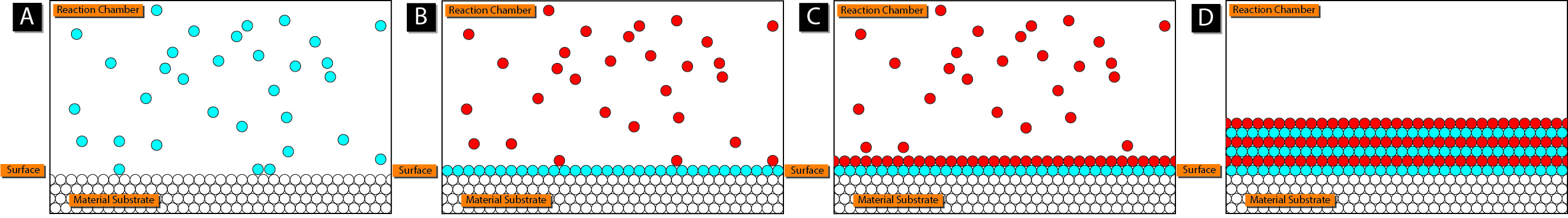
Figure 6. Schematic of the cyclical two-step ALD process. (Reprinted from Mcat chem446, CC BY-SA 3.0, via Wikimedia Commons)
The ALD process also does not require very high temperatures, which means that it could be the solution for the BEOL CMOS integration of 2D materials [78]. There has already been a demonstration of the successful growth of ML and bulk MoS2 using ALD at 300 °C using MoCl5 and H2S precursors for Mo and S, respectively [79][80]. The major concern with ALD is that the deposition conditions, including the substrate material, have been shown to significantly impact the nucleation and growth of the films [81].
An additional concern with the integration of 2D materials with CMOS technology is the difficulty in patterning the films, which will be critically damaged if exposed to plasma etching. A recent study by Ahn et al. [82] showed that it was possible to simultaneously deposit and etch MoS2 layers using MoCl5 and H2S precursors at 400 °C. Essentially, the authors show a selective deposition process, whereby the Mo-precursor MoCl5 would not adsorb onto the SiO2 surface, while adsorbing onto the surface areas which were covered by aluminum, even after 400 ALD cycles.
3.2. Gas Sensing Principles of 2D Materials
The main sensing mechanism of SMO sensors is through the surface adsorption of oxygen ions, such as O2−, O−, and O2− [83]. The presence of the oxygen ions on the surface create a depletion region, which is then reduced when these ions react with gas molecules of interest. Therein lies the core of the sensing mechanism for SMOs: For n-type sensing materials (e.g., SnO2, ZnO, TiO2) the resistance will decrease or increase, depending on if it is exposed to reducing or oxidizing gases, respectively. The inverse is the case when a p-type SMO material is used (e.g., CuO, NiO, Cr2O3). For gas sensors based on 2D materials, however, the process does not require oxygen adsorption and the mechanism mainly follows the charge-transfer process [30]. This means that the sensing film will act as a donor or acceptor of charges from the adsorbed gas molecule during the charge transfer procedure. Since different gases are able to exchange charges with the 2D film, it is the amount of charge that is exchanged, leading to changes in the conductive behavior of the film, that can be used to classify the specificity of the gas sensor. It should also be noted that the adsorption of gas molecules on the monolayer surface of a 2D semiconductor typically results in a change in its band structure. The adsorbed molecule could introduce additional energy states, giving rise to a shift in the Fermi level.
4. 2D-Material-Based Gas Sensing Films
The change in the conductivity of graphene and other 2D materials as a result of a changing make-up of the ambient environment is already proven, and publications in this direction are plentiful. Even as early as 2007, the Nobel laureates for graphene’s fabrication and characterization (i.e., Geim and Novoselov [55]) described and reported on graphene’s changing electrical properties due to exposure to NO2 and NH3 [91]. Specifically, they showed that the adsorbed molecules increased the charge carrier density of graphene, with paramagnetic molecules such as NO2 acting as an electron dopant. However, due to graphene’s lack of a band gap, researchers have been unable to develop a functional digital logic FET. As a result, other possible 2D materials have gained momentum, which exhibit the presence of a reasonably large band gap while also having tremendous potential for concurrent FET, optical, and sensing applications.
4.1. Graphene Oxide and Reduced Graphene Oxide
4.2. Transition Metal Dichalcogenides
4.3. Phosphorene
4.3.1. Black Phosphorene
4.3.2. Blue Phosphorene
4.4. MXenes
4.5. Two-Dimensional Heterojunctions
There has been significant interest recently in the application of 2D heterostructures in order to increase the sensitivity or selectivity of the thin 2D layers towards gas sensing [152][153]. The use of heterostructures is not new and has also been applied to SMO-based chemiresistive sensors in the past [154][155].
4.5.1. Fabrication of 2D Heterostructures
4.5.2. Gas Sensing with 2D Heterostructures
4.5.3. Illuminated 2D Heterojunction Gas Sensors
References
- Filipovic, L.; Lahlalia, A. System-on-chip SMO gas sensor integration in advanced CMOS technology. J. Electrochem. Soc. 2018, 165, B862–B879.
- Korotcenkov, G. Metal oxides for solid-state gas sensors: What determines our choice? Mater. Sci. Eng. B 2007, 139, 1–23.
- Dey, A. Semiconductor metal oxide gas sensors: A review. Mater. Sci. Eng. B 2018, 229, 206–217.
- Filipovic, L.; Selberherr, S. Thermo-electro-mechanical simulation of semiconductor metal oxide gas sensors. Materials 2019, 12, 2410.
- Liu, X.; Cheng, S.; Liu, H.; Hu, S.; Zhang, D.; Ning, H. A survey on gas sensing technology. Sensors 2012, 12, 9635–9665.
- Ponzoni, A.; Baratto, C.; Cattabiani, N.; Falasconi, M.; Galstyan, V.; Nunez-Carmona, E.; Rigoni, F.; Sberveglieri, V.; Zambotti, G.; Zappa, D. Metal oxide gas sensors, a survey of selectivity issues addressed at the SENSOR Lab, Brescia (Italy). Sensors 2017, 17, 714.
- SGX SENSORTECH. MiCS-6814: MOS Triple Sensor; SGX SENSORTECH: Neuchatel, Switzerland, 2007.
- ams AG. AS-MLV-P2 Air Quality Sensor; ams AG: Premstatten, Austria, 2015.
- Figaro USA, Inc. TGS 8100—For the Detection of Air Contaminants; Figaro USA, Inc.: Arlington Heights, IL, USA, 2014.
- Figaro USA, Inc. TGS 2602—For the Detection of Air Contaminants; Figaro USA, Inc.: Arlington Heights, IL, USA, 2015.
- Figaro USA, Inc. TGS 2600—For the Detection of Air Contaminants; Figaro USA, Inc.: Arlington Heights, IL, USA, 2013.
- ams AG. Ultra-Low Power Digital Gas Sensor for Monitoring Indoor Air Quality, CCS811:v1-00; ams AG: Premstatten, Austria, 2016.
- ams AG. Ultra-Low Power Analog Gas Sensor for Ethanol Detection, CCS803:v1-00; ams AG: Premstatten, Austria, 2016.
- ams AG. Ultra-Low Power Analog VOC Sensor for Indoor Air Quality Monitoring, CCS801:v1-02; ams AG: Premstatten, Austria, 2016.
- Ghosh, R.; Gardner, J.W.; Guha, P.K. Air pollution monitoring using near room temperature resistive gas sensors: A review. IEEE Trans. Electron Devices 2019, 66, 3254–3264.
- Zhao, Y.; Song, J.G.; Ryu, G.H.; Ko, K.Y.; Woo, W.J.; Kim, Y.; Kim, D.; Lim, J.H.; Lee, S.; Lee, Z.; et al. Low-temperature synthesis of 2D MoS2 on a plastic substrate for a flexible gas sensor. Nanoscale 2018, 10, 9338–9345.
- Venkateshalu, S.; Grace, A.N. MXenes-A new class of 2D layered materials: Synthesis, properties, applications as supercapacitor electrode and beyond. Appl. Mater. Today 2020, 18, 100509.
- Cao, J.; Chen, Q.; Wang, X.; Zhang, Q.; Yu, H.D.; Huang, X.; Huang, W. Recent development of gas sensing platforms based on 2D atomic crystals. Research 2021, 2021, 9863038.
- Rigoni, F.; Pintossi, C.; Drera, G.; Pagliara, S.; Lanti, G.; Castrucci, P.; Crescenzi, M.D.; Sangaletti, L. A cross-functional nanostructured platform based on carbon nanotube-Si hybrid junctions: Where photon harvesting meets gas sensing. Sci. Rep. 2017, 7, 44413.
- Lee, D.Y.; Yu, J.B.; Byun, H.G.; Kim, H.J. Chemoresistive sensor readout circuit design for detecting gases with slow response time characteristics. Sensors 2022, 22, 1102.
- Akinwande, D.; Huyghebaert, C.; Wang, C.H.; Serna, M.I.; Goossens, S.; Li, L.J.; Wong, H.S.P.; Koppens, F.H. Graphene and two-dimensional materials for silicon technology. Nature 2019, 573, 507–518.
- Romijn, J.; Vollebregt, S.; van Zeijl, H.W.; Sarro, P.M. A wafer-scale process for the monolithic integration of CVD graphene and CMOS logic for smart MEMS/NEMS sensors. In Proceedings of the 2019 IEEE 32nd International Conference on Micro Electro Mechanical Systems (MEMS), Seoul, Korea, 27–31 January 2019; IEEE: Piscataway, NJ, USA, 2019.
- Pilotto, A.; Khakbaz, P.; Palestri, P.; Esseni, D. Semi-classical transport in MoS2 and MoS2 transistors by a Monte Carlo approach. Solid-State Electron. 2022, 192, 108295.
- Han, S.J.; Garcia, A.V.; Oida, S.; Jenkins, K.A.; Haensch, W. Graphene radio frequency receiver integrated circuit. Nat. Commun. 2014, 5, 3086.
- Schöning, M.J.; Poghossian, A. Recent advances in biologically sensitive field-effect transistors (BioFETs). Analyst 2002, 127, 1137–1151.
- Sung, D.; Koo, J. A review of BioFET’s basic principles and materials for biomedical applications. Biomed. Eng. Lett. 2021, 11, 85–96.
- Martinoia, S.; Massobrio, G.; Lorenzelli, L. Modeling ISFET microsensor and ISFET-based microsystems: A review. Sens. Actuators B Chem. 2005, 105, 14–27.
- Keeble, L.; Moser, N.; Rodriguez-Manzano, J.; Georgiou, P. ISFET-based sensing and electric field actuation of DNA for on-chip detection: A review. IEEE Sens. J. 2020, 20, 11044–11065.
- Zhang, J.; Liu, L.; Yang, Y.; Huang, Q.; Li, D.; Zeng, D. A review on two-dimensional materials for chemiresistive- and FET-type gas sensors. Phys. Chem. Chem. Phys. 2021, 23, 15420–15439.
- Wang, B.; Gu, Y.; Chen, L.; Ji, L.; Zhu, H.; Sun, Q. Gas sensing devices based on two-dimensional materials: A review. Nanotechnology 2022, 33, 252001.
- Liu, Y.; Duan, X.; Shin, H.J.; Park, S.; Huang, Y.; Duan, X. Promises and prospects of two-dimensional transistors. Nature 2021, 591, 43–53.
- Schram, T.; Smets, Q.; Heyne, M.; Graven, B.; Kunnen, E.; Thiam, A.; Devriendt, K.; Delabie, A.; Lin, D.; Chiappe, D.; et al. BEOL compatible WS2 transistors fully fabricated in a 300 mm pilot line. In Proceedings of the 2017 Silicon Nanoelectronics Workshop (SNW), Kyoto, Japan, 4–5 June 2017; IEEE: Piscataway, NJ, USA, 2017.
- Kozhakhmetov, A.; Nasr, J.R.; Zhang, F.; Xu, K.; Briggs, N.C.; Addou, R.; Wallace, R.; Fullerton-Shirey, S.K.; Terrones, M.; Das, S.; et al. Scalable BEOL compatible 2D tungsten diselenide. 2D Mater. 2019, 7, 015029.
- Pace, S.; Ferrera, M.; Convertino, D.; Piccinini, G.; Magnozzi, M.; Mishra, N.; Forti, S.; Bisio, F.; Canepa, M.; Fabbri, F.; et al. Thermal stability of monolayer WS2 in BEOL conditions. J. Phys. Mater. 2021, 4, 024002.
- Xiang, D.; Liu, T. Monolayer transistors at wafer scales. Nat. Electron. 2021, 4, 868–869.
- Schram, T.; Sutar, S.; Radu, I.; Asselberghs, I. Challenges of wafer-scale integration of 2D semiconductors for high-performance transistor circuits. Adv. Mater. 2022, 2109796.
- Yokosawa, K.; Saitoh, K.; Nakano, S.; Goto, Y.; Tsukada, K. FET hydrogen-gas sensor with direct heating of catalytic metal. Sens. Actuators B Chem. 2008, 130, 94–99.
- Hong, S.; Hong, Y.; Jeong, Y.; Jung, G.; Shin, W.; Park, J.; Lee, J.K.; Jang, D.; Bae, J.H.; Lee, J.H. Improved CO gas detection of Si MOSFET gas sensor with catalytic Pt decoration and pre-bias effect. Sens. Actuators B Chem. 2019, 300, 127040.
- Schierbaum, K.; Kirner, U.; Geiger, J.; Göpel, W. Schottky-barrier and conductivity gas sensors based upon Pd/SnO2 and Pt/TiO2. Sens. Actuators B Chem. 1991, 4, 87–94.
- Adrian, A.R.; Cerda, D.; Fernández-Izquierdo, L.; Segura, R.A.; García-Merino, J.A.; Hevia, S.A. Tunable low crystallinity carbon nanotubes/silicon Schottky junction arrays and their potential application for gas sensing. Nanomaterials 2021, 11, 3040.
- Ano, T.; Kishimoto, F.; Tsubaki, S.; Lu, Y.H.; Hohman, J.N.; Maitani, M.M.; Salmeron, M.; Wada, Y. Controlling the Schottky barrier at the Pt/TiO2 interface by intercalation of a self-assembled monolayer with oriented dipole moments. J. Phys. Chem. C 2021, 125, 13984–13989.
- Pohle, R.; Simon, E.; Schneider, R.; Fleischer, M.; Meixner, H.; Frerichs, H.P.; Lehmann, M. Realization of a new sensor concept: Improved CCFET and SGFET type gas sensors in Hybrid Flip-Chip technology. In Proceedings of the TRANSDUCERS ’03. 12th International Conference on Solid-State Sensors, Actuators and Microsystems. Digest of Technical Papers (Cat. No.03TH8664), Boston, MA, USA, 8–12 June 2003; IEEE: Piscataway, NJ, USA, 2003; pp. 135–138.
- Waltl, M.; Knobloch, T.; Tselios, K.; Filipovic, L.; Stampfer, B.; Hernandez, Y.; Waldhör, D.; Illarionov, Y.; Kaczer, B.; Grasser, T. Perspective of 2D integrated electronic circuits: Scientific pipe dream or disruptive technology? Adv. Mater. 2022, 2201082.
- Uchida, K.; Watanabe, H.; Kinoshita, A.; Koga, J.; Numata, T.; Takagi, S. Experimental study on carrier transport mechanism in ultrathin-body SOI nand p-MOSFETs with SOI thickness less than 5 nm. In Proceedings of the Digest. International Electron Devices Meeting, San Francisco, CA, USA, 8–11 December 2002; IEEE: Piscataway, NJ, USA, 2002; pp. 47–50.
- da Silva, M.B.; Tuinhout, H.; van Duijnhoven, A.Z.; Wirth, G.I.; Scholten, A. A physics-based RTN variability model for MOSFETs. In Proceedings of the IEEE International Electron Devices Meeting, San Francisco, CA, USA, 15–17 December 2014; IEEE: Piscataway, NJ, USA, 2014; pp. 35.2.1–35.2.4.
- Deng, D.; Novoselov, K.S.; Fu, Q.; Zheng, N.; Tian, Z.; Bao, X. Catalysis with two-dimensional materials and their heterostructures. Nat. Nanotechnol. 2016, 11, 218–230.
- Rivera-Cárcamo, C.; Serp, P. Single atom catalysts on carbon-based materials. ChemCatChem 2018, 10, 5058–5091.
- Zhao, S.; Chen, G.; Zhou, G.; Yin, L.C.; Veder, J.P.; Johannessen, B.; Saunders, M.; Yang, S.Z.; Marco, R.D.; Liu, C.; et al. A universal seeding strategy to synthesize single atom catalysts on 2D materials for electrocatalytic applications. Adv. Funct. Mater. 2019, 30, 1906157.
- Gusmão, R.; Veselý, M.; Sofer, Z. Recent developments on the single atom supported at 2D materials beyond graphene as catalysts. ACS Catal. 2020, 10, 9634–9648.
- Kumar, R.; Liu, X.; Zhang, J.; Kumar, M. Room-temperature gas sensors under photoactivation: From metal oxides to 2D materials. Nano-Micro Lett. 2020, 12, 164.
- Yang, S.; Jiang, C.; Wei, S.h. Gas sensing in 2D materials. Appl. Phys. Rev. 2017, 4, 021304.
- Rohaizad, N.; Mayorga-Martinez, C.C.; Fojtů, M.; Latiff, N.M.; Pumera, M. Two-dimensional materials in biomedical, biosensing and sensing applications. Chem. Soc. Rev. 2021, 50, 619–657.
- Filipovic, L.; Selberherr, S. Gas sensing with two-dimensional materials beyond graphene. In Proceedings of the 2021 IEEE 32nd International Conference on Microelectronics (MIEL), Nis, Serbia, 12–14 September 2021; IEEE: Piscataway, NJ, USA, 2021; pp. 29–36.
- Knobloch, T. On the Electrical Stability of 2D Material-Based Field-Effect Transistors. Ph.D. Thesis, TU Wien, Vienna, Austria, 2022.
- Novoselov, K.S.; Geim, A.K.; Morozov, S.V.; Jiang, D.; Zhang, Y.; Dubonos, S.V.; Grigorieva, I.V.; Firsov, A.A. Electric field effect in atomically thin carbon films. Science 2004, 306, 666–669.
- Knobloch, T.; Grasser, T.; Selberherr, S. Challenges for nanoscale CMOS logic based on two-dimensional materials. Nanomaterials 2022, 12, 3548.
- Knobloch, T.; Selberherr, S.; Grasser, T. Challenges for Nanoscale CMOS Logic Based on Two-Dimensional Materials. Nanomaterials 2022, 12, 3548. https://doi.org/10.3390/nano12203548
- Shi, Y.; Li, H.; Wong, J.I.; Zhang, X.; Wang, Y.; Song, H.; Yang, H.Y. MoS2 surface structure tailoring via carbonaceous promoter. Sci. Rep. 2015, 5, 10378.
- Ryder, C.R.; Wood, J.D.; Wells, S.A.; Hersam, M.C. Chemically tailoring semiconducting two-dimensional transition metal dichalcogenides and black phosphorus. ACS Nano 2016, 10, 3900–3917.
- Kang, K.; Xie, S.; Huang, L.; Han, Y.; Huang, P.Y.; Mak, K.F.; Kim, C.J.; Muller, D.; Park, J. High-mobility three-atom-thick semiconducting films with wafer-scale homogeneity. Nature 2015, 520, 656–660.
- Cun, H.; Macha, M.; Kim, H.; Liu, K.; Zhao, Y.; LaGrange, T.; Kis, A.; Radenovic, A. Wafer-scale MOCVD growth of monolayer MoS2 on sapphire and SiO2. Nano Res. 2019, 12, 2646–2652.
- Walsh, L.A.; Hinkle, C.L. Van der Waals epitaxy: 2D materials and topological insulators. Appl. Mater. Today 2017, 9, 504–515.
- Zhou, X.; Kang, K.; Xie, S.; Dadgar, A.; Monahan, N.R.; Zhu, X.Y.; Park, J.; Pasupathy, A.N. Atomic-scale spectroscopy of gated monolayer MoS2. Nano Lett. 2016, 16, 3148–3154.
- Pang, X.; Zhang, Q.; Shao, Y.; Lui, M.; Zhang, D.; Zhao, Y.; A flexible pressure sensor based on magnetron sputtered MoS2. Sensors 2021, 21, 1130, 10.3390/s21041130.
- Greene, J.E. Review Article: Tracing the recorded history of thin-film sputter deposition: From the 1800s to 2017. J. Vac. Sci. Technol. A Vac. Surfaces Film. 2017, 35, 05C204.
- Muratore, C.; Voevodin, A.A.; Glavin, N.R. Physical vapor deposition of 2D Van der Waals materials: A review. Thin Solid Film. 2019, 688, 137500.
- Huang, J.H.; Chen, H.H.; Liu, P.S.; Lu, L.S.; Wu, C.T.; Chou, C.T.; Lee, Y.J.; Li, L.J.; Chang, W.H.; Hou, T.H. Large-area few-layer MoS2 deposited by sputtering. Mater. Res. Express 2016, 3, 065007.
- Samassekou, H.; Alkabsh, A.; Wasala, M.; Eaton, M.; Walber, A.; Walker, A.; Pitkänen, O.; Kordas, K.; Talapatra, S.; Jayasekera, T.; et al. Viable route towards large-area 2D MoS2 using magnetron sputtering. 2D Mater. 2017, 4, 021002.
- Voevodin, A.A.; Waite, A.R.; Bultman, J.E.; Hu, J.; Muratore, C. Magnetic field argon ion filtering for pulsed magnetron sputtering growth of two-dimensional MoS2. Surf. Coatings Technol. 2015, 280, 260–267.
- Chen, X.; Xing, G.; Xu, L.; Lian, H.; Wang, Y. Vertically aligned MoS2 films prepared by RF-magnetron sputtering method as electrocatalysts for hydrogen evolution reactions. Compos. Interfaces 2020, 28, 707–716.
- Villamayor, M.M.S.; Lindblad, A.; Johansson, F.O.; Tran, T.; Pham, N.H.; Primetzhofer, D.; Sorgenfrei, N.L.; Giangrisotomi, E.; Föhlisch, A.; Lourenço, P.; et al. Growth of two-dimensional WS2 thin films by reactive sputtering. Vacuum 2021, 188, 110205.
- Manzeli, S.; Ovchinnikov, D.; Pasquier, D.; Yazyev, O.V.; Kis, A. 2D transition metal dichalcogenides. Nat. Rev. Mater. 2017, 2, 17033.
- Yang, P.; Zhang, S.; Pan, S.; Tang, B.; Liang, Y.; Zhao, X.; Zhang, Z.; Shi, J.; Huan, Y.; Shi, Y.; et al. Epitaxial growth of centimeter-scale single-crystal MoS2 monolayer on Au(111). ACS Nano 2020, 14, 5036–5045.
- Cheng, P.; Zhang, W.; Zhang, L.; Gou, J.; Wong, P.K.J.; Chen, L. Molecular beam epitaxy fabrication of two-dimensional materials. In 2D Semiconductor Materials and Devices; Elsevier: Amsterdam, The Netherlands, 2020; pp. 103–134.
- Thomas, J.; Bradford, J.; Cheng, T.S.; Summerfield, A.; Wrigley, J.; Mellor, C.J.; Khlobystov, A.N.; Foxon, C.T.; Eaves, L.; Novikov, S.V.; et al. Step-flow growth of graphene-boron nitride lateral heterostructures by molecular beam epitaxy. 2D Mater. 2020, 7, 035014.
- Ugeda, M.M.; Bradley, A.J.; Shi, S.F.; da Jornada, F.H.; Zhang, Y.; Qiu, D.Y.; Ruan, W.; Mo, S.K.; Hussain, Z.; Shen, Z.X.; et al. Giant bandgap renormalization and excitonic effects in a monolayer transition metal dichalcogenide semiconductor. Nat. Mater. 2014, 13, 1091–1095.
- Hao, W.; Marichy, C.; Journet, C. Atomic layer deposition of stable 2D materials. 2D Mater. 2018, 6, 012001.
- Xu, X.; Guo, T.; Kim, H.; Hota, M.K.; Alsaadi, R.S.; Lanza, M.; Zhang, X.; Alshareef, H.N. Growth of 2D materials at the wafer scale. Adv. Mater. 2022, 34, 2108258.
- Tan, L.K.; Liu, B.; Teng, J.H.; Guo, S.; Low, H.Y.; Loh, K.P. Atomic layer deposition of a MoS2 film. Nanoscale 2014, 6, 10584–10588.
- Sreedhara, M.B.; Gope, S.; Vishal, B.; Datta, R.; Bhattacharyya, A.J.; Rao, C.N.R. Atomic layer deposition of crystalline epitaxial MoS2 nanowall networks exhibiting superior performance in thin-film rechargeable Na-ion batteries. J. Mater. Chem. A 2018, 6, 2302–2310.
- Groven, B.; Mehta, A.N.; Bender, H.; Meersschaut, J.; Nuytten, T.; Verdonck, P.; Conard, T.; Smets, Q.; Schram, T.; Schoenaers, B.; et al. Two-dimensional crystal grain size tuning in WS2 atomic layer deposition: An insight in the nucleation mechanism. Chem. Mater. 2018, 30, 7648–7663.
- Ahn, W.; Lee, H.; Kim, H.; Leem, M.; Lee, H.; Park, T.; Lee, E.; Kim, H. Area-selective atomic layer deposition of MoS2 using simultaneous deposition and etching characteristics of MoCl2. Phys. Status Solidi (RRL)-Rapid Res. Lett. 2021, 15, 2000533.
- Degler, D.; Wicker, S.; Weimar, U.; Barsan, N. Identifying the active oxygen species in SnO2 based gas sensing materials: An operando IR spectrsocopy study. J. Phys. Chem. C 2015, 119, 11792–11799.
- González, C.; Biel, B.; Dappe, Y.J. Adsorption of small inorganic molecules on a defective MoS2 monolayer. Phys. Chem. Chem. Phys. 2017, 19, 9485–9499.
- Babar, V.; Vovusha, H.; Schwingenschlögl, U. Density functional theory analysis of gas adsorption on monolayer and few layer transition metal dichalcogenides: Implications for sensing. ACS Appl. Nano Mater. 2019, 2, 6076–6080.
- González, C.; Biel, B.; Dappe, Y.J. Theoretical characterisation of point defects on a MoS2 monolayer by scanning tunnelling microscopy. Nanotechnology 2016, 27, 105702.
- Linghu, Y.; Wu, C. Gas molecules on defective and nonmetal-doped MoS2 monolayers. J. Phys. Chem. C 2019, 124, 1511–1522.
- Wang, X.; Zhang, Y.; Si, H.; Zhang, Q.; Wu, J.; Gao, L.; Wei, X.; Sun, Y.; Liao, Q.; Zhang, Z.; et al. Single-atom vacancy defect to trigger high-efficiency hydrogen evolution of MoS2. J. Am. Chem. Soc. 2020, 142, 4298–4308.
- Wu, A.; Song, Q.; Liu, H. Oxygen atom adsorbed on the sulphur vacancy of monolayer MoS2: A promising method for the passivation of the vacancy defect. Comput. Theor. Chem. 2020, 1187, 112906.
- Enujekwu, F.M.; Zhang, Y.; Ezeh, C.I.; Zhao, H.; Xu, M.; Besley, E.; George, M.W.; Besley, N.A.; Do, H.; Wu, T. N-doping enabled defect-engineering of MoS2 for enhanced and selective adsorption of CO2: A DFT approach. Appl. Surf. Sci. 2021, 542, 148556.
- Schedin, F.; Geim, A.; Morozov, S.; Hill, E.; Blake, P.; Katsnelson, M.; Novoselov, K. Detection of individual gas molecules adsorbed on graphene. Nat. Mater. 2007, 6, 652.
- Wang, C.; Zhang, L.; Guo, Z.; Xu, J.; Wang, H.; Zhai, K.; Zhuo, X. A novel hydrazine electrochemical sensor based on the high specific surface area graphene. Microchim. Acta 2010, 169, 1–6.
- Toda, K.; Furue, R.; Hayami, S. Recent progress in applications of graphene oxide for gas sensing: A review. Anal. Chim. Acta 2015, 878, 43–53.
- Tarcan, R.; Todor-Boer, O.; Petrovai, I.; Leordean, C.; Astilean, S.; Botiz, I. Reduced graphene oxide today. J. Mater. Chem. C 2020, 8, 1198–1224.
- Donarelli, M.; Ottaviano, L. 2D materials for gas sensing applications: A review on graphene oxide, MoS2, WS2 and phosphorene. Sensors 2018, 18, 3638.
- Hummers, W.S.; Offeman, R.E. Preparation of graphitic oxide. J. Am. Chem. Soc. 1958, 80, 1339.
- Perera, S.D.; Mariano, R.G.; Vu, K.; Nour, N.; Seitz, O.; Chabal, Y.; Balkus, K.J. Hydrothermal synthesis of graphene-TiO2 nanotube composites with enhanced photocatalytic activity. ACS Catal. 2012, 2, 949–956.
- Chen, J.; Yao, B.; Li, C.; Shi, G. An improved Hummers method for eco-friendly synthesis of graphene oxide. Carbon 2013, 64, 225–229.
- Borini, S.; White, R.; Wei, D.; Astley, M.; Haque, S.; Spigone, E.; Harris, N.; Kivioja, J.; Ryhänen, T. Ultrafast graphene oxide humidity sensors. ACS Nano 2013, 7, 11166–11173.
- Huang, X.; Leng, T.; Georgiou, T.; Abraham, J.; Nair, R.R.; Novoselov, K.S.; Hu, Z. Graphene oxide dielectric permittivity at GHz and its applications for wireless humidity sensing. Sci. Rep. 2018, 8, 43.
- Sun, C.; Shi, Q.; Yazici, M.; Lee, C.; Liu, Y. Development of a highly sensitive humidity sensor based on a piezoelectric micromachined ultrasonic transducer array functionalized with graphene oxide thin film. Sensors 2018, 18, 4352.
- Shen, F.; Wang, D.; Liu, R.; Pei, X.; Zhang, T.; Jin, J. Edge-tailored graphene oxide nanosheet-based field effect transistors for fast and reversible electronic detection of sulfur dioxide. Nanoscale 2013, 5, 537–540.
- Kim, Y.H.; Park, J.S.; Choi, Y.R.; Park, S.Y.; Lee, S.Y.; Sohn, W.; Shim, Y.S.; Lee, J.H.; Park, C.R.; Choi, Y.S.; et al. Chemically fluorinated graphene oxide for room temperature ammonia detection at ppb levels. J. Mater. Chem. A 2017, 5, 19116–19125.
- Wang, Y.; Zhang, L.; Hu, N.; Wang, Y.; Zhang, Y.; Zhou, Z.; Liu, Y.; Shen, S.; Peng, C. Ammonia gas sensors based on chemically reduced graphene oxide sheets self-assembled on Au electrodes. Nanoscale Res. Lett. 2014, 9, 251.
- Lu, G.; Ocola, L.E.; Chen, J. Reduced graphene oxide for room-temperature gas sensors. Nanotechnology 2009, 20, 445502.
- Wang, D.H.; Hu, Y.; Zhao, J.J.; Zeng, L.L.; Tao, X.M.; Chen, W. Holey reduced graphene oxide nanosheets for high performance room temperature gas sensing. J. Mater. Chem. A 2014, 2, 17415–17420.
- Reddeppa, M.; Park, B.G.; Kim, M.D.; Peta, K.R.; Chinh, N.D.; Kim, D.; Kim, S.G.; Murali, G. H2, H2S gas sensing properties of rGO/GaN nanorods at room temperature: Effect of UV illumination. Sens. Actuators B Chem. 2018, 264, 353–362.
- Pal, P.; Yadav, A.; Chauhan, P.S.; Parida, P.K.; Gupta, A. Reduced graphene oxide based hybrid functionalized films for hydrogen detection: Theoretical and experimental studies. Sens. Int. 2021, 2, 100072.
- Robinson, J.T.; Perkins, F.K.; Snow, E.S.; Wei, Z.; Sheehan, P.E. Reduced graphene oxide molecular sensors. Nano Lett. 2008, 8, 3137–3140.
- Li, X.; Zhu, H. Two-dimensional MoS2: Properties, preparation, and applications. J. Mater. 2015, 1, 33–44.
- Chen, Y.; Deng, W.; Chen, X.; Wu, Y.; Shi, J.; Zheng, J.; Chu, F.; Liu, B.; An, B.; You, C.; et al. Carrier mobility tuning of MoS2 by strain engineering in CVD growth process. Nano Res. 2020, 14, 2315–2320.
- Kumar, R.R.; Habib, M.R.; Khan, A.; Chen, P.C.; Murugesan, T.; Gupta, S.; kumar Anbalagan, A.; Tai, N.H.; Lee, C.H.; Lin, H.N. Sulfur monovacancies in liquid-exfoliated MoS2 nanosheets for NO2 gas sensing. ACS Appl. Nano Mater. 2021, 4, 9459–9470.
- Wang, Q.H.; Kalantar-Zadeh, K.; Kis, A.; Coleman, J.N.; Strano, M.S. Electronics and optoelectronics of two-dimensional transition metal dichalcogenides. Nat. Nanotechnol. 2012, 7, 699–712.
- Rezende, N.P.; Cadore, A.R.; Gadelha, A.C.; Pereira, C.L.; Ornelas, V.; Watanabe, K.; Taniguchi, T.; Ferlauto, A.S.; Malachias, A.; Campos, L.C.; et al. Probing the electronic properties of monolayer MoS2 via interaction with molecular hydrogen. Adv. Electron. Mater. 2019, 5, 1800591.
- Tong, Y.; Lin, Z.; Thong, J.T.; Chan, D.S.; Zhu, C. MoS2 oxygen sensor with gate voltage stress induced performance enhancement. Appl. Phys. Lett. 2015, 107, 123105.
- Shokri, A.; Salami, N. Gas sensor based on MoS2 monolayer. Sens. Actuators B Chem. 2016, 236, 378–385.
- Salih, E.; Ayesh, A.I. First principle study of transition metals codoped MoS2 as a gas sensor for the detection of NO and NO2 gases. Phys. E Low-Dimens. Syst. Nanostruct. 2021, 131, 114736.
- Li, Y.; Song, Z.; Li, Y.; Chen, S.; Li, S.; Li, Y.; Wang, H.; Wang, Z. Hierarchical hollow MoS2 microspheres as materials for conductometric NO2 gas sensors. Sens. Actuators B Chem. 2019, 282, 259–267.
- Järvinen, T.; Lorite, G.S.; Peräntie, J.; Toth, G.; Saarakkala, S.; Virtanen, V.K.; Kordas, K. WS2 and MoS2 thin film gas sensors with high response to NH3 in air at low temperature. Nanotechnology 2019, 30, 405501.
- Park, J.; Mun, J.; Shin, J.S.; Kang, S.W. Highly sensitive two-dimensional MoS2 gas sensor decorated with Pt nanoparticles. R. Soc. Open Sci. 2018, 5, 181462.
- Pereira, N.M.; Rezende, N.P.; Cunha, T.H.R.; Barboza, A.P.M.; Silva, G.G.; Lippross, D.; Neves, B.R.A.; Chacham, H.; Ferlauto, A.S.; Lacerda, R.G. Aerosol-printed MoS2 ink as a high sensitivity humidity sensor. ACS Omega 2022, 7, 9388–9396.
- Zhang, L.; Khan, K.; Zou, J.; Zhang, H.; Li, Y. Recent advances in emerging 2D material-based gas sensors: Potential in disease diagnosis. Adv. Mater. Interfaces 2019, 6, 1901329.
- Yu, Z.G.; Zhang, Y.W.; Yakobson, B.I. An anomalous formation pathway for dislocation-sulfur vacancy complexes in polycrystalline monolayer MoS2. Nano Lett. 2015, 15, 6855–6861.
- Li, Q.; Zheng, S.; Pu, J.; Wang, W.; Li, L.; Wang, L. Revealing the failure mechanism and designing protection approach for MoS2 in humid environment by first-principles investigation. Appl. Surf. Sci. 2019, 487, 1121–1130.
- Chen, D.; Zhang, X.; Tang, J.; Cui, H.; Li, Y. Noble metal (Pt or Au)-doped monolayer MoS2 as a promising adsorbent and gas-sensing material to SO2, SOF2 and SO2F2: A DFT study. Appl. Phys. A 2018, 124, 194.
- Abbasi, A.; Sardroodi, J.J. Adsorption of O3, SO2 and SO3 gas molecules on MoS2 monolayers: A computational investigation. Appl. Surf. Sci. 2019, 469, 781–791.
- Zhang, G.; Wang, Z.; Zhang, X. Theoretical screening into Ru-doped MoS2 monolayer as a promising gas sensor upon SO2 and SOF2 in SF6 insulation devices. Mol. Phys. 2021, 120, e2018517.
- Li, B.; Zhou, Q.; Peng, R.; Liao, Y.; Zeng, W. Adsorption of SF6 decomposition gases (H2S, SO2, SOF2 and SO2F2) on Sc-doped MoS2 surface: A DFT study. Appl. Surf. Sci. 2021, 549, 149271.
- Hou, W.; Mi, H.; Peng, R.; Peng, S.; Zeng, W.; Zhou, Q. First-principle insight into Ga-doped MoS2 for sensing SO2, SOF2 and SO2F2. Nanomaterials 2021, 11, 314.
- Liu, D.; Guo, Y.; Fang, L.; Robertson, J. Sulfur vacancies in monolayer MoS2 and its electrical contacts. Appl. Phys. Lett. 2013, 103, 183113.
- Cho, K.; Min, M.; Kim, T.Y.; Jeong, H.; Pak, J.; Kim, J.K.; Jang, J.; Yun, S.J.; Lee, Y.H.; Hong, W.K.; et al. Electrical and optical characterization of MoS2 with sulfur vacancy passivation by treatment with alkanethiol molecules. ACS Nano 2015, 9, 8044–8053.
- Burman, D.; Raha, H.; Manna, B.; Pramanik, P.; Guha, P.K. Substitutional doping of MoS2 for superior gas-sensing applications: A proof of concept. ACS Sens. 2021, 6, 3398–3408.
- Bharathi, P.; Harish, S.; Mathankumar, G.; Mohan, M.K.; Archana, J.; Kamalakannan, S.; Prakash, M.; Shimomura, M.; Navaneethan, M. Solution processed edge activated Ni-MoS2 nanosheets for highly sensitive room temperature NO2 gas sensor applications. Appl. Surf. Sci. 2022, 600, 154086.
- Guo, Z.; Zhang, H.; Lu, S.; Wang, Z.; Tang, S.; Shao, J.; Sun, Z.; Xie, H.; Wang, H.; Yu, X.F.; et al. From black phosphorus to phosphorene: Basic solvent exfoliation, evolution of raman scattering, and applications to ultrafast photonics. Adv. Funct. Mater. 2015, 25, 6996–7002.
- Liu, H.; Neal, A.T.; Zhu, Z.; Luo, Z.; Xu, X.; Tománek, D.; Ye, P.D. Phosphorene: An unexplored 2D semiconductor with a high hole mobility. ACS Nano 2014, 8, 4033–4041.
- Castellanos-Gomez, A.; Vicarelli, L.; Prada, E.; Island, J.O.; Narasimha-Acharya, K.L.; Blanter, S.I.; Groenendijk, D.J.; Buscema, M.; Steele, G.A.; Alvarez, J.V.; et al. Isolation and characterization of few-layer black phosphorus. 2D Mater. 2014, 1, 025001.
- Pei, J.; Gai, X.; Yang, J.; Wang, X.; Yu, Z.; Choi, D.Y.; Luther-Davies, B.; Lu, Y. Producing air-stable monolayers of phosphorene and their defect engineering. Nat. Commun. 2016, 7, 10450.
- Abbas, A.N.; Liu, B.; Chen, L.; Ma, Y.; Cong, S.; Aroonyadet, N.; Köpf, M.; Nilges, T.; Zhou, C. Black phosphorus gas sensors. ACS Nano 2015, 9, 5618–5624.
- Cai, Y.; Ke, Q.; Zhang, G.; Zhang, Y.W. Energetics, charge transfer, and magnetism of small molecules physisorbed on phosphorene. J. Phys. Chem. C 2015, 119, 3102–3110.
- Mansouri, E.; Karamdel, J.; Berahman, M.; Ahmadi, M.T. Phosphorene as H2S and CH4 gas sensor. Phys. Status Solidi (a) 2018, 216, 1800086.
- Zeng, J.; Cui, P.; Zhang, Z. Half layer by half layer growth of a blue phosphorene monolayer on a GaN(001) substrate. Phys. Rev. Lett. 2017, 118, 046101.
- Xiao, J.; Long, M.; Deng, C.S.; He, J.; Cui, L.L.; Xu, H. Electronic structures and carrier mobilities of blue phosphorus nanoribbons and nanotubes: A first-principles study. J. Phys. Chem. C 2016, 120, 4638–4646.
- Safari, F.; Fathipour, M.; Goharrizi, A.Y. Electronic and transport properties of blue phosphorene in presence of point defects: A first-principles study. Phys. E Low-Dimens. Syst. Nanostruct. 2020, 118, 113938.
- Sun, S.; Hussain, T.; Zhang, W.; Karton, A. Blue phosphorene monolayers as potential nano sensors for volatile organic compounds under point defects. Appl. Surf. Sci. 2019, 486, 52–57.
- Chen, G.X.; Wang, R.X.; Li, H.X.; Chen, X.N.; An, G.; Zhang, J.M. First-principles study of pristine and metal decorated blue phosphorene for sensing toxic H2S, SO2 and NO2 molecules. Appl. Phys. A 2021, 127, 133.
- Niu, F.; Yang, D.; Cai, M.; Li, X.; Liu, D. A first principles study of blue phosphorene as a superior media for gas sensor. In Proceedings of the 19th International Conference on Electronic Packaging Technology (ICEPT), Shanghai, China, 8–11 August 2018; IEEE: Piscataway, NJ, USA, 2018.
- Meshginqalam, B.; Barvestani, J. Vacancy defected blue and black phosphorene nanoribbons as gas sensor of NOx and SOx molecules. Appl. Surf. Sci. 2020, 526, 146692.
- Akkuş, Ü.Ö.; Balcı, E.; Berber, S. Device characteristics of Ti2CT2 MXene-based field-effect transistor. Superlattices Microstruct. 2020, 140, 106433.
- Naguib, M.; Kurtoglu, M.; Presser, V.; Lu, J.; Niu, J.; Heon, M.; Hultman, L.; Gogotsi, Y.; Barsoum, M.W. Two-dimensional nanocrystals produced by exfoliation of Ti3AlC2. Adv. Mater. 2011, 23, 4248–4253.
- Bhardwaj, R.; Hazra, A. MXene-based gas sensors. J. Mater. Chem. C 2021, 9, 15735–15754.
- Devaraj, M.; Rajendran, S.; Hoang, T.K.; Soto-Moscoso, M. A review on MXene and its nanocomposites for the detection of toxic inorganic gases. Chemosphere 2022, 302, 134933.
- Bag, A.; Lee, N.E. Gas sensing with heterostructures based on two-dimensional nanostructured materials: A review. J. Mater. Chem. C 2019, 7, 13367–13383.
- Li, Z.; Yao, Z.; Haidry, A.A.; Luan, Y.; Chen, Y.; Zhang, B.Y.; Xu, K.; Deng, R.; Hoa, N.D.; Zhou, J.; et al. Recent advances of atomically thin 2D heterostructures in sensing applications. Nano Today 2021, 40, 101287.
- Alam, M.W.; Pooja, P.; Aamir, M.; Souayeh, B.; Mushtaq, S.; Khan, M.S.; Amin, M.N.; Khan, K.; Shajahan, S. The recent development in chemoresistive-rased heterostructure gas sensor technology, their future opportunities and challenges: A review. Membranes 2022, 12, 555.
- Singh, A.; Sikarwar, S.; Verma, A.; Yadav, B.C. The recent development of metal oxide heterostructures based gas sensor, their future opportunities and challenges: A review. Sens. Actuators A Phys. 2021, 332, 113127.
- Gong, Y.; Lin, J.; Wang, X.; Shi, G.; Lei, S.; Lin, Z.; Zou, X.; Ye, G.; Vajtai, R.; Yakobson, B.I.; et al. Vertical and in-plane heterostructures from WS2/MoS2 monolayers. Nat. Mater. 2014, 13, 1135–1142.
- Li, B.; Huang, L.; Zhong, M.; Li, Y.; Wang, Y.; Li, J.; Wei, Z. Direct vapor phase growth and optoelectronic application of large band offset SnS2/MoS2 vertical bilayer heterostructures with high lattice mismatch. Adv. Electron. Mater. 2016, 2, 1600298.
- Cui, Y.; Li, B.; Li, J.; Wei, Z. Chemical vapor deposition growth of two-dimensional heterojunctions. Sci. China Phys. Mech. Astron. 2017, 61, 16801.
- Zhang, Z.; Chen, P.; Duan, X.; Zang, K.; Luo, J.; Duan, X. Robust epitaxial growth of two-dimensional heterostructures, multiheterostructures, and superlattices. Science 2017, 357, 788–792.
- Poh, S.M.; Zhao, X.; Tan, S.J.R.; Fu, D.; Fei, W.; Chu, L.; Jiadong, D.; Zhou, W.; Pennycook, S.J.; Neto, A.H.C.; et al. Molecular beam epitaxy of highly crystalline MoSe2 on hexagonal boron nitride. ACS Nano 2018, 12, 7562–7570.
- Cho, B.; Yoon, J.; Lim, S.K.; Kim, A.R.; Kim, D.H.; Park, S.G.; Kwon, J.D.; Lee, Y.J.; Lee, K.H.; Lee, B.H.; et al. Chemical sensing of 2D graphene/MoS2 heterostructure device. ACS Appl. Mater. Interfaces 2015, 7, 16775–16780.
- Cho, B.; Yoon, J.; Lim, S.; Kim, A.; Choi, S.Y.; Kim, D.H.; Lee, K.; Lee, B.; Ko, H.; Hahm, M. Metal decoration effects on the gas-sensing properties of 2D hybrid-structures on flexible substrates. Sensors 2015, 15, 24903–24913.
- Zheng, W.; Xu, Y.; Zheng, L.; Yang, C.; Pinna, N.; Liu, X.; Zhang, J. MoS2 van der Waals p-n junctions enabling highly selective room-temperature NO2 sensor. Adv. Funct. Mater. 2020, 30, 2000435.

