The SMO-based gas sensor, considered the current workhorse of semiconductor-based chemiresistive gas sensor technologies, requires high temperatures to initiate the surface reactions which result in the sensing response, making it difficult to fabricate and prone to high mechanical instability. Therefore, alternatives at lower temperatures are desired, where 2D materials seem to hold the most promise. Even at ambient temperature, their sensitivity is extraordinarily large due to their extremely high surface-to-volume ratio. However, some ongoing issues still need to be resolved before gas sensors based on 2D materials can be widely used and commercialized. The alternative room temperature solutions involve optical signals, either by designing an NDIR sensor based on the Beer-Lambert law or by introducing an additional UV illumination to SMO sensors. In both cases, CMOS integration is not feasible, which is why continued interest in 2D-material-based gas sensors persists.
1. Gas Sensing Technologies
A large set of materials for gas sensing and gas sensor designs are under investigation and find themselves at vastly different maturity levels of realizable development. Several advanced gas sensing technologies which have already been commercialized by industry include electrochemical (EC) sensors, catalytic pellistors (CP), thermal pellistors (TP), piezo-electric (PE) sensors, photo-ionization (PI) devices, optical infrared (IR) adsorption sensors, and semiconductor metal oxide (SMO) chemiresistors [9,23,24,25]. These technologies are typically divided into two categories: One whose detection mechanism is based on changing a material’s electrical behavior after adsorption (e.g., conductivity, field effect) and a second whose detection depends on an induced change in another property (e.g., thermal, optical) [26].
The semiconductor-based chemiresistive technology provides an option with the lowest cost, footprint, and power dissipation, mainly as a consequence of its successful integration with complementary metal oxide semiconductor (CMOS) fabrication techniques. These characteristics are necessary in order to enable sensing solutions for portable technologies as well as IoE and IoT integration, while integration with CMOS further ensures a means for very high and reliable reproducibility [27]. It is crucial for the volume manufacturing of commercial devices that there be minimal inter-device variances and that there is high confidence in the capability to produce a device with predictable attributes and highly manageable tolerances. We also observe a low power dissipation attributed to the catalytic pellistor which is also inexpensive to manufacture and has a comparatively small physical footprint. However, compared to the SMO sensor, this device has far worse selectivity, lesser sensitivity, and a slower reaction time. Piezoelectric, photo-ionization, and infrared sensors all offer excellent sensitivity, but they all have the drawback of high power consumption, which prevents portability and internet-of-things (IoT) integration.
In comparison to existing alternatives, the SMO sensor appears to provide the most benefits towards potential IoT applications. Previous research has shown that it has several advantages leading to its commercialization [30,31,32,33,34,35,36,37], particularly in terms of response time, sensitivity, and possibilities for portability and down-scaling. The high sensitivity of SMO sensors is, however, only made possible by applying very high operating temperatures, which may compromise their reliability and durability. With the goal of CMOS integration for a chemiresistive gas sensing solution, the SMO sensor has emerged as the industry standard. A semiconductor-based approach, which operates at ambient temperature and can be designed with established CMOS fabrication techniques is, therefore, highly desired. Several sensors and prospective sensing materials, including two-dimensional (2D) semiconductors such as graphene and transition metal dichalcogenides (TMDs), are being investigated in this direction [38]. The fabrication of these films, and devices based on these films, is not trivial. Nevertheless, investigations in the past few years have shown some promise in fabricating films of high quality for sensing and have made significant progress [39,40].
2. Semiconductor-Based Gas Sensor Types
2.1. Chemiresistors
For chemiresistors, the electrical resistance of the sensor changes as a consequence of the adsorption of gas molecules on its surface. The sensitivity
S towards a particular gas is, therefore, determined by how much the resistance of the film changes after exposure to this gas, usually starting from a baseline using operating conditions in pure ambient air. However, it should be noted that some studies use inert ambient, e.g., N
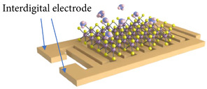
2, as the baseline resistance, which is why it is often difficult to truly compare sensitivities across a broad set of experimental literature studies. From all of the available types of semiconductor-based gas sensors, the chemiresistor is the easiest to fabricate, since it only requires placing the sensing film on top of an insulating substrate and adding two metal contacts, which are often formed using interdigitated electrodes, as shown in the figure (Reprinted with permission from Cao et al. [
109],
CC-BY 4.0). The read-out circuit for the chemiresistive gas sensor is also quite straight-forward since only the current flowing through the resistor needs to be measured, which can be performed by placing a load resistor and reading the voltage across it [
122,
123]. The ease of chemiresistive gas sensor fabrication brings about the potential for their cost-efficient fabrication, ability of scaling, and eventual CMOS integration.
The key to introducing a new material for chemiresistive gas sensing in a CMOS technology relies on its integration with the back-end-of-line (BEOL) process [
124]. The front-end-of-line (FEOL) is primarily reserved for manipulating the silicon wafer in the form of doping and implantation in order to form transistors for memory and digital logic. During BEOL fabrication, the metallization and interconnections between the FEOL devices are created, which is why it is more convenient to introduce new materials, as there is already sufficient insulation to the silicon wafer and metallization is available. Therefore, in principle, it should be relatively easy to introduce a new material, such as a 2D layer within the BEOL steps. However, one major problem is that most studies which are performed on 2D materials for chemiresistive gas sensing on a silicon wafer rely on a thermally grown SiO
2 interface to the 2D film. Thermally growing SiO
2 during BEOL is not permissible, since there is a strict thermal budget which must be followed during these steps, and the temperature must not exceed about 400 °C. Therefore, alternatives must be found, such as plasma-enhanced chemical vapor deposition (PECVD)-grown SiO
2 or SiN insulation on top of which the 2D film is placed [
125]. Alternatively, new insulating materials could be introduced in the CMOS flow, but this may further complicate the fabrication, adding more time and cost. The fact that it is not clear which insulator and 2D material combination would make the most feasible integration is an additional concern, since it has become abundantly clear that the choice of insulator plays a very important role in the electrical properties of the 2D film due to the introduction of surface optical phonon scattering, which becomes the dominant scattering effect, limiting the film’s conductivity [
126]. It is therefore not clear what impact the rougher PECVD surface will have on the electrical and sensing properties of the chemiresistive film. One option is to introduce a chemical mechanical polishing (CMP) step in the BEOL process to smoothen the insulator surface before introducing the 2D film, something similar to what was proposed by Han et al. in [
127]. Nevertheless, a thorough investigation of all materials which contact the 2D film will have to be made before the relatively simple integration of 2D materials for chemiresistive gas sensors are introduced in the BEOL.
2.2. Field Effect Transistors
The field-effect transistor (FET) is the workhorse of the semiconductor industry and is the cornerstone of digital logic and many memory devices. In addition, the field effect, as implemented in a FET or a metal-oxide-semiconductor FET (MOSFET), has been extensively used in advanced bio-sensing technologies with the biologically sensitive field-effect transistor (BioFET) [
128,
129] and ion-sensitive field-effect transistor (ISFET) [
130,
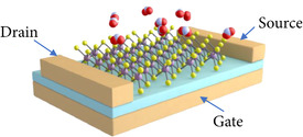
131] designs. These devices provide a means to adjust the electrostatics of the channel layer using an electrode, which is suspended in an electrolyte solution, which is in contact with the gate dielectric. The sensitivity of the BioFET and ISFET structures are governed by how the charge accumulation changes on the gate dielectric and the selectivity is introduced by placing immobilized receptors on top the gate, which will only react to specific bio-molecules. However, generating such a structure, which has a high sensitivity and selectivity, for gas sensing is more challenging. In bio-sensors and BioFETs the electrolyte serves to keep undesired molecules out of the gate or channel regions. For gas sensors, on the other hand, exposing the channel to the ambient means it is exposed to any molecule which may come in its vicinity, shown in figure (Reprinted with permission from Cao et al. [
109],
CC-BY 4.0).
From the different types of FET-based gas sensing structures, the thin-film transistor (TFT) appears to be the most promising option and has been tested most extensively using 2D semiconductor materials [
114,
121]. The reason is that it is relatively easy to fabricate test devices, and the sensitive 2D film is the one which is directly exposed to the gas and acts as a FET channel layer. While this device seems promising for CMOS integration, the fact that it requires a back-gate is a concern. Incorporating a back-gate on a wafer-scale makes it difficult (or impossible) to control the electrostatics of each transistor’s gate independently. Therefore, for CMOS integration, once again, BEOL compatible solutions are being investigated [
132,
133,
134,
135,
136,
137].
The catalytic FET sensor works on the principle that the work function of the gate metal, such as palladium, platinum, or gold, changes when exposed to an increased concentration of certain gases. Most often, these are small gas molecules such as H
2 [
138] or CO [
139]. The H
2 adsorbs on the outer surface of the metal gate and dissociates into H atoms which then diffuse through the catalytic metal gate, moving downward towards its interface with the insulator. At the interface, a dipole layer is formed, changing the surface potential of the gate and shifting the threshold voltage V
t of the FET. This feature of the catalytic metal films is also used at the main sensing principle in Schottky-barrier gas sensors [
140,
141,
142]. Furthermore, it should also be noted that these types of sensors are relatively easy to integrate with CMOS fabrication, albeit the inclusion of catalytic metals such as gold or platinum can be problematic. However, their major limitation is that they can only be used to detect very small molecules, preventing their broad applicability for gas sensing of hazardous air pollutants or for bio-sensing of volatile organic compounds (VOCs) in exhaled breath for medical applications.
Since the catalytic FET sensor is limited to detecting only small gas molecules which are able to diffuse through the metal layer, capacitively-coupled FET (CCFET) and suspended gate FET (SGFET) structures have been proposed. These devices include an air gap between the gate insulator and sensing layer, whereby larger molecules are also accessible. The air gap, however, makes fabrication very difficult, often requiring flip-chip technology, which complicates potential scaling, mass production, and CMOS integration [
143].
3. Fabrication and Working Principle of 2D-Material-Based Gas Sensors
The semiconductor industry is clearly dominated by silicon, and the introduction of new applications and technologies on silicon is usually a stepping stone towards mass production and adoption in the market. Over the years, many materials have attempted to replace silicon, including materials with higher charge carrier mobility, such as germanium, and various group III-IV materials. However, none have been successful in commercialization on a broad scale and have only made breakthroughs in certain niche markets [22]. The continued scaling of silicon appears to have reached saturation and sub-3 nm channels pose significant challenges due to increased variability and reliability issues, but also due to the limited carrier mobility at these reduced scales [149,150].
Beyond transistor scaling and digital logic, interest in 2D materials has intensified over the past years due to their potential usability in a wide range of applications. Due to the low dimensionality of these materials, they exhibit properties of relevance to several research fields from solid-state physics to low dimensional molecular chemistry. Therefore, even minor shifts in the chemical structure of the film’s surface can be felt in its bulk properties. This feature makes 2D materials ideal for catalysis [152,153,154,155] and sensing [93,156,157]. The range of application for gas sensing is immense and includes devices which are able to detect hazardous gases, organic vapors, and humidity: Devices frequently used for medical diagnostics, environmental monitoring, and safety and security [157]. TMDs including MoS2, MoTe2, WSe2, and SnS2 have already been widely studied for gas sensing in the FET configuration, primarily for the detection of nitrogen-containing compounds. In the chemiresistor configuration, a broader group of 2D materials have shown high potential for gas sensor development, including TMDs, boron nitride, black phosphorus, and MXenes [1,121].
3.1. Synthesis of 2D Materials
A thorough review of the means by which 2D materials are synthesized is provided by Knobloch in [164]. Here, we look at these processes from the perspective of their CMOS integration. The initial discovery of 2D materials for electronic applications was enabled by the mechanical exfoliation of single or few layers of graphene from a layered bulk crystal graphite [151]. While this process is not scalable and does not lend itself to CMOS integration, it is still frequently used in lab-based research into 2D materials and devices due to the simplicity of the process and the reasonable quality of films which can be achieved. The process involves thinning down a thick layer of a 2D crystal by placing it on adhesive tape. Subsequently, by frequently folding and unfolding the tape, increasingly fewer layers remain. These layers are then transferred to a wafer, typically SiO2-on-silicon [164,165,[1]].
3.1.1. Chemical Vapor Deposition
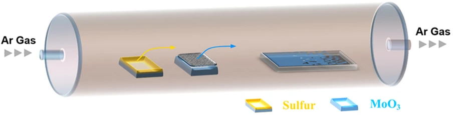
Chemical vapor deposition (CVD) is probably the most widely studied means of depositing a film and is a staple of the microelectronics industry and of a CMOS foundry. It is a relatively simple bottom-up growth process which offers flexibility of metal precursor and a relatively fast growth rate. Several studies have examined the growth of graphene, hexagonal Boron Nitride (hBN), and TMDs using CVD, while only a few studies have looked into growing black phosphorene with this method. This has to do with black phosphorus’ tendency to quickly oxidize in the presence of oxygen, requiring an oxygen-free growth environment. Furthermore, a precursor is required to grow the material. For MoS
2, the precursor is the chalgogen sulfur, as shown in the above figure (Reprinted with permission from Shi et al. [
166],
CC-BY 4.0); for phosphorene, this would be phosphine, which is a highly toxic material [
171].
A variation on CVD, mainly metal-organic chemical vapor deposition (MOCVD), has also been used recently to grow 2D semiconductors [
172]. This process uses gaseous metal–organic compounds as precursors instead of the solids in powder form used during CVD. This provides the advantage of temperature reduction down to a BEOL-compatible 450 °C, and the precise control over the partial pressures of all precursors grown in the chamber, which can now be introduced using mass flow controllers [
173,
174]. While this process has shown excellent yield and layer uniformity, it comes with a high density of trap states in the deposited films [
175]. In fact, single-crystalline layers of 2D materials have, to date, not been successfully grown using MOCVD [
164].
3.1.2. Physical Vapor Deposition
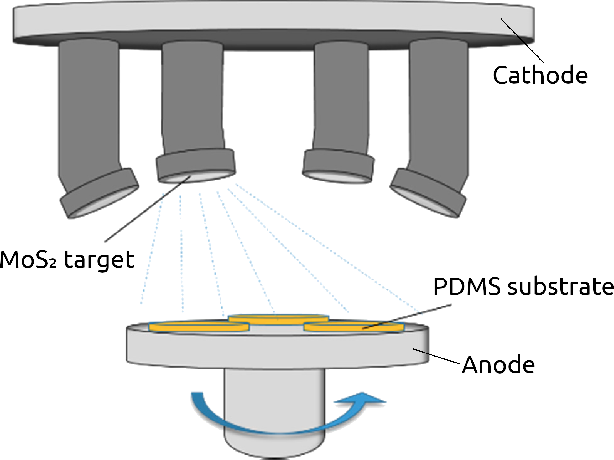
A typical alternative to CVD in a CMOS foundry is physical vapor deposition (PVD) which most often refers to thermal evaporation deposition or sputtering. PVD belongs to a family of synthesis processes which enable large-scale processing of 2D van der Waals (vdW) materials. The figure shows such a setup for the sputtering of MoS2 films from a target (Reprinted with permission from Pang et al. [2], CC-BY 4.0). There is no fundamental limit on the size or shape of the films which can be generated using this process, which has been used to produce thicker vdW films for decades [176,177], while the deposition of a few layers has also been recently demonstrated [178,179]. PVD also does not require the transfer of the grown material onto the desired substrate, as growth on any substrate is inherently possible.
The main principle behind sputtering is that a chunk of the target material is bombarded by ions from a gaseous plasma, whereby small sections of said material (down to single atoms) is sputtered off of the target. These sputtered particles then travel through the chamber, ultimately depositing onto the desired substrate. A magnetic source is often integrated with the target in order to confine the electrons to the regions close to the target’s surface. This type of sputtering is called magnetron sputtering, and it can be used to sputter any film, regardless of its melting temperature. Magnetron sputtering has been used to deposit both MoS
2 [
181,
182] and WS
2 films [
183]. The major concern with sputtered 2D films is that the material which is deposited is polycrystalline and often sub-stoichiometric [
181]. The high polycrystallinity leads to very low charge mobilities, in the order of 0.0136 cm
2V
−1s
−1 and 0.0564 cm
2V
−1s
−1 for bi-layer and five-layer MoS
2, respectively [
178]. The mobility can be brought up to about 10 cm
2V
−1s
−1 after a high-temperature annealing step, which is still far below the mobilities achieved for CVD- or MBE-grown films [
177]. Annealing the film at high temperatures would then negate the benefits that sputtering would initially provide for CMOS integration.
3.1.3. Molecular-Beam Epitaxy
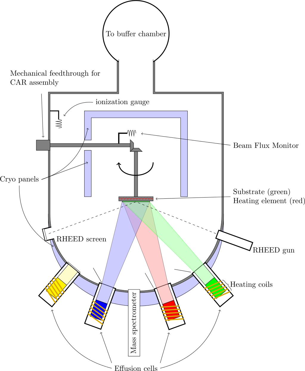
Molecular-beam epitaxy (MBE) is a process by which epitaxial growth can be performed on a large scale in an ultra-high vacuum chamber with pressures in the sub 10−10 mbar range [184] and a typical MBE setup is shown in the above figure (Reprinted from Vegar Ottesen, CC BY 3.0, via Wikimedia Commons). In MBE, the precursor molecules form a film on a heated crystalline substrate, which only provides the crystallographic information for the formation of the new film [164]. Since the substrate does not provide any catalytic surface effects, MBE results in a direct in situ growth of vertically-stacked heterostructures [185].
MBE is a very powerful tool for growing high-quality crystalline 2D films and has been extensively used to realize many films, including graphene, TMDs, and elemental 2D materials [187]. In addition, MBE has been applied to grow vertical and lateral vdW heterostructures [188]. There are, however, several difficulties in integrating MBE within a CMOS technology flow. The high vacuum requirements and high process sensitivity to small variations are a particular concern for mass production. Therefore, the technology remains principally a research tool for studying the fundamental properties of various material systems [189].
3.1.4. Atomic Layer Deposition
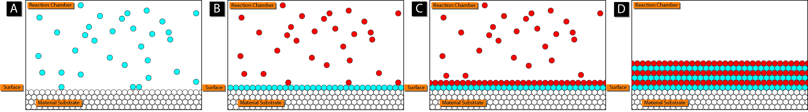
Atomic layer deposition (ALD) is a method of thin film deposition which offers more control over film conformality and thickness than traditional CVD. A typical multi-step ALD flow is shown in the above figure (Mcat chem446, CC BY-SA 3.0, via Wikimedia Commons). Because it may be used to deposit technologically important oxides and nitrides, such as the gate oxide HfO2 and gate metal TiN, ALD has emerged as a fundamental technique in semiconductor processing for advanced nodes. This is primarily due to the self-limiting nature of the process. In simple terms, ALD requires at least two self-limiting steps, during which different gases are allowed to interact with the surface, in order to ultimately initiate the deposition of a single monolayer of a material. During each step, a surface catalytic reaction takes place, which ensures that the surface is covered with a specific precursor. This precursor then only reacts with the species which enters the chamber in the second step, thereby forming the desired film. In this way, ALD can be used to grow very precise thin films with excellent conformality and thickness control down to the angstrom level [192].
The ALD process also does not require very high temperatures, which means that it could be the solution for the BEOL CMOS integration of 2D materials [193]. There has already been a demonstration of the successful growth of ML and bulk MoS2 using ALD at 300 °C using MoCl5 and H2S precursors for Mo and S, respectively [194,195]. The major concern with ALD is that the deposition conditions, including the substrate material, have been shown to significantly impact the nucleation and growth of the films [196].
An additional concern with the integration of 2D materials with CMOS technology is the difficulty in patterning the films, which will be critically damaged if exposed to plasma etching. A recent study by Ahn et al. [198] showed that it was possible to simultaneously deposit and etch MoS2 layers using MoCl5 and H2S precursors at 400 °C. Essentially, the authors show a selective deposition process, whereby the Mo-precursor MoCl5 would not adsorb onto the SiO2 surface, while adsorbing onto the surface areas which were covered by aluminum, even after 400 ALD cycles.
3.2. Gas Sensing Principles of 2D Materials
The main sensing mechanism of SMO sensors is through the surface adsorption of oxygen ions, such as O2−, O−, and O2− [199]. The presence of the oxygen ions on the surface create a depletion region, which is then reduced when these ions react with gas molecules of interest. Therein lies the core of the sensing mechanism for SMOs: For n-type sensing materials (e.g., SnO2, ZnO, TiO2) the resistance will decrease or increase, depending on if it is exposed to reducing or oxidizing gases, respectively. The inverse is the case when a p-type SMO material is used (e.g., CuO, NiO, Cr2O3). For gas sensors based on 2D materials, however, the process does not require oxygen adsorption and the mechanism mainly follows the charge-transfer process [121]. This means that the sensing film will act as a donor or acceptor of charges from the adsorbed gas molecule during the charge transfer procedure. Since different gases are able to exchange charges with the 2D film, it is the amount of charge that is exchanged, leading to changes in the conductive behavior of the film, that can be used to classify the specificity of the gas sensor. It should also be noted that the adsorption of gas molecules on the monolayer surface of a 2D semiconductor typically results in a change in its band structure. The adsorbed molecule could introduce additional energy states, giving rise to a shift in the Fermi level.
These material systems and interactions with gas molecules are typically studied using
ab initio calculations [
207,
208]. The interactions, when the 2D material is pristine and not defected, depend mostly on vdW interactions between the gas molecule and the film. However, these weak forces alone were unable to explain many observed changes in the electrical properties of 2D semiconductors under varying ambient conditions [
207,
208]. These changes are proposed to be induced by the interactions between the gas molecules and point defects in the 2D semiconductor. Many defects are noted at the edges and grain boundaries, while an atomic mono-vacancy can readily appear also in the surface of a crystalline film [
209]. Several studies have taken to first principles simulations in order to understand the interactions between gas molecules and differently defected 2D semiconductor surfaces [
207,
212,
213,
214,
215].
4. 2D-Material-Based Gas Sensing Films
The change in the conductivity of graphene and other 2D materials as a result of a changing make-up of the ambient environment is already proven, and publications in this direction are plentiful. Even as early as 2007, the Nobel laureates for graphene’s fabrication and characterization (i.e., Geim and Novoselov [151]) described and reported on graphene’s changing electrical properties due to exposure to NO2 and NH3 [216]. Specifically, they showed that the adsorbed molecules increased the charge carrier density of graphene, with paramagnetic molecules such as NO2 acting as an electron dopant. However, due to graphene’s lack of a band gap, researchers have been unable to develop a functional digital logic FET. As a result, other possible 2D materials have gained momentum, which exhibit the presence of a reasonably large band gap while also having tremendous potential for concurrent FET, optical, and sensing applications.
4.1. Graphene Oxide and Reduced Graphene Oxide
Considerable attention has been attracted by graphene recently for various applications. This is most likely due to it being the breakthrough 2D material, which was fabricated and investigated at its monolayer the earliest. Graphene was shown to be particularly interesting for gas sensing applications due to its extremely high specific surface area, which interacts with certain gases to change the film’s physical properties [
217]. However, its near-zero band gap is a significant hurdle for its broad applicability in transistors and sensing devices. Therefore, many researchers began investigating functionalized or decorated graphene using graphene oxide (GO) [
218,
219]. Strong oxidizers can be used to treat graphite in order to separate the graphite from the GO flakes. Through subsequent graphite exfoliation, only the GO flakes remain [
220]. The modified Hummers’ method [
221,
222,
223] is the primary means applied to generate wider GO flakes with a lower number of defects, with the hopes of increasing the production yield.
Graphene oxide (GO) is an analog of graphene with many functional groups which ensure that the physical and chemical properties of the film are significantly different to that of graphene [
218]. The material exhibits a very high resistivity, while its permittivity is often affected by the ambient, which is why so many capacitive sensors are designed with GO as the sensing layer. In order to partially recover the highly conductive behavior of pristine graphene films for chemiresistive sensors, the GO layers are typically reduced, generating reduced GO (rGO) flakes [
219]. Reduced graphene oxide (rGO) is synthesized from GO and is often treated as graphene in publications and discussions. However, a key difference is that rGO sheets, like GO, are inexpensive and easy to prepare while having the benefit of a large surface-to-volume ratio. Reduced graphene oxide can also be tailored to exhibit properties from insulating (i.e., near-GO) to near-metallic (i.e., fully reduced GO will theoretically produce graphene), depending on the process used to reduce GO.
GO flakes have been readily applied for the fabrication of an impedance sensor for the detection of relative humidity (RH) [
224]. The real and imaginary components of the GO’s dielectric constant are used in these investigations as a sensing signal [
225]. Molecular surface adsorption causes the dielectric constant to fluctuate, which in-turn causes the frequency response to alter, thereby shifting the resonant frequency which can be detected. For fast and precise RH detection, this mechanism has been recently used in a piezoelectric micromachined ultrasonic transducer, combined with a GO sensing layer [
226].
Surface functionalization techniques have readily been applied for the fabrication of SMO-based sensors. This is a common method to engineer additional sensitivity and selectivity and improve the overall performance of chemiresistive gas sensors. Researchers have been investigating the potential of functionalizing and micromachining the GO surface to improve its sensing performance and, in particular, to ensure selectivity/specificity towards a particular gas molecule [
220]. For instance, to improve specific SO
2 and NH
3 detection at room temperature, specially tailored GO flakes have been fabricated, as described in [
237] and [
238], respectively.
Because of the increased conductivity of rGO films and due to the presence of hydroxyl groups on their surface, which facilitate adsorption, these materials have been extensively researched for their potential use in gas sensing devices [
121,
220]. The degree of reduction can also be tuned and adjusted to tailor the film’s applicability towards a specific use-case. Many important gases and compounds can be detected using these films, even at ambient temperature. For example, rGO flakes have been used for the detection of NH
3 at concentrations ranging from 5 ppb to 100 ppm [
239], NO
2 for concentrations at ppb levels [
240,
241], hydrogen at ppm levels [
242,
243], and even chemical warfare agents down to the ppb level [
244].
4.2. Transition Metal Dichalcogenides
MoS
2 and WS
2, in their bulk forms, are made up of several S–Mo–S or S–W–S planes, respectively, connected to each other through van der Waals forces. Researchers have demonstrated that these films can be synthesized using CVD [
269,
270], while they can also be exfoliated down to a monolayer (ML) thickness [
271]. The bulk forms of MoS
2 and WS
2 films show indirect semiconductor performance, with band gaps of around 1.2 eV and 1 eV, respectively. The ML alternatives of these materials, however, are direct semiconductors and exhibit band gaps of 1.8 eV and 2 eV, respectively [
272].
MoS
2 has already been demonstrated to respond quite strongly to the presence of many gases of interest, even at room temperature, e.g., H
2 [
273], O
2 [
274], NO [
275,
276], NO
2 [
276,
277], NH
3 [
278], H
2S [
279], humidity [
280], and many more. MoS
2 is shown to readily react and change its conductive behavior due to a change in humidity or oxygen concentration in the ambient air, meaning that hydroxil groups and oxygen readily adsorb on its surface. This may be a hindrance in the future wide application of MoS
2 in microelectronic devices and sensors, as the presence of humidity and oxygen is unavoidable, especially when it comes to selective exhaled breath detection [
206]. Furthermore, polycristalline MoS
2 layers have been shown to exhibit high defect concentrations on their edges and at the grain boundaries, where gas molecules can frequently adsorb [
203,
204]. It should be noted that theoretical studies on the potential of MoS
2 for the detection of a wide variety of gas molecules are abound [
281,
282,
283,
284,
285].
The substitutional doping of TMD monolayers most often proceeds by populating an already existing vacancy, most often a sulfur or selenide vacancy, which is created as a result of the material synthesis. In the MoS
2 example, sulfur vacancies can readily appear during fabrication or exfoliation [
210,
296]. These vacancies then serve as favorable adsorption sites for the metal dopant atoms [
291]. Because these vacancies form during the exfoliation process a method has been proposed to replace these vacancies with a desired metal atom directly during exfoliation [
291]. However, there is still a long way to go before mass production of such films can be realized. One recently studied alternative to vacancy doping is edge activation [
297]. Essentially, TMD monolayers deposit as flakes and the edges of these flakes may contain several vacancies or dangling bonds, which can then be used as adsorption sites for metal atoms or gas molecules directly [
297].
4.3. Phosphorene
Phosphorene refers to the ML of phosphorus and several allotropes of phosphorene have been investigated recently in their potential capacity for gas sensing. The most prominent one, which has also been investigated for the longest time due to the fact that it was synthesized the earliest, is black phosphorene. In fact, “phosphorene” usually is assumed to refer to “black phosphorene”. However, recently, blue and green phosphorene have also drawn attention in their potential use towards gas sensing applications. While there are claims being made with regards to fabricated blue phosphorene, most studies surrounding both blue and green allotropes are theoretical and rely on first-principles calculations.
4.3.1. Black Phosphorene
A monolayer (ML) of black phosphorus is commonly referred to as black phosphorene, or even simply phosphorene. The film possesses a honeycomb structure, while demonstrating p-type conductivity with a high carrier mobility and a band gap somewhere in the range of 0.3 eV and 1.9 eV, depending on the process used for its synthesis [
315,
316]. Much like several TMDs, black phosphorene has already been employed in the fabrication and testing of FETs [
317,
318] as well as for gas sensing applications [
319]. It has been demonstrated using
ab initio density functional theory (DFT) calculations that molecules such as CO, H
2, H
2O, and NH
3 behave as electron donors, while NO, NO
2, and O
2 operate as electron acceptors, when adsorbed on the phosphorene surface [
320]. While
ab initio techniques have shown some propensity of H
2 and CH
4 adsorption on phosphorene [
321], NO
2 appears to exhibit the strongest interactions with the surface of the phosphorene film, highlighting its promise for future gas detector applications [
220]. A black-phosphorus-based FET, according to experimental observations in [
319], is capable of detecting levels of NO
2 as low as 5 ppm in an argon environment, but the device’s response time is quite slow, i.e., on the scale of several minutes. The recovery time was shown to be even longer, taking over 30 min.
4.3.2. Blue Phosphorene
In the last few years, interest in blue phosphorene has significantly increased, most likely due to claims of its successful synthesis. Blue phosphorene is an allotrope of black phosphorus, which is formed by a single layer of phosphorus atoms more flatly arranged than in the case of black phosphorene [
328]. A monolayer of blue phosphorene was theoretically shown to exhibit a carrier mobility of over 1000 cm
2V
−1s
−1 [
329] (the mobility of MoS
2 is about 200 cm
2V
−1s
−1, for comparison). Blue phosphorene also exhibits a fundamental indirect band gap of about 2 eV, which can be modified to a direct band gap through doping [
330]. Blue phosphorene has been studied as a medium for gas sensing using first principles calculations in several studies [
330,
331,
332]. First principles studies suggest that blue phosphorene can be an effective gas sensor using its pristine surface [
333] in addition to an increased adsorption and sensitivity potential of phosphorus vacancy sites [
327]. Further studies suggest that specific doping can improve sensitivity and selectivity towards desired molecules [
330,
332]. Recent research suggest that covalent bonds do not form between small gas molecules (e.g., H
2O, SO
2, NH
3, H
2S, O
2) on pristine blue phosphorene and that physical adsorption takes place. The authors in [
333] suggest that the physical adsorption of gas molecules can be used to tune the band gap of blue phosphorene and its work function. However, strong adsorption and significant changes occur as a result of adsorption on vacancy defects, which was recently described for NO
x and SO
x sensing [
327].
4.4. MXenes
MXenes are a class of 2D inorganic compounds with a narrow band gap on the order of about 0.2 eV [
345]. The material consists of a few-atoms-thick layer of transition metal carbides, nitrides, or carbonitrides. The first such film, namely, 2D Ti
3C
2, was synthesized in 2011 by Naguib et al. [
346] by exfoliating Ti
3AlC
2. The exfoliation process includes replacing Al atoms with OH after immersion in HF and subsequent reactions. The hydrogen bonds are then broken, and the nanosheet is separated after sonication in methanol.
MXenes have merged onto the ever-increasing scene of 2D materials relatively recently, especially when compared to graphene and TMDs. However, this younger member of the 2D materials family has attracted significant attention for its physical, chemical, and electronic properties, which may be suitable for many relevant applications [
347]. When considering MXene films for gas sensing, investigations have shown that they enhance chemical functionality for gas adsorption while enjoying the benefits of large surface-to-volume ratio, as noted with other 2D materials [
348].
4.5. Two-Dimensional Heterojunctions
There has been significant interest recently in the application of 2D heterostructures in order to increase the sensitivity or selectivity of the thin 2D layers towards gas sensing [363,364]. The use of heterostructures is not new and has also been applied to SMO-based chemiresistive sensors in the past [365,366].
4.5.1. Fabrication of 2D Heterostructures
It should be noted that any stacking of multiple 2D materials introduces further fabrication complexity and reduces the probability of time- and cost-efficient CMOS integration. However, there have been reports of controllable fabrication of 2D heterostructures using mechanical stacking or direct-growth methods [
364]. While mechanical stacking is not a process which can easily be incorporated in a CMOS foundry, direct-growth methods using CVD have better potential here [
367,
368,
369]. To date, a wide variety of 2D heterostructures have been fabricated using CVD with a wide ranging set of properties which are shown to depend on specific parameters of the process itself, such as the type of species, the precursor dosage, the type and flow rate of the carrier gas, the temperature, and the duration of the chemical reaction. Nevertheless, a comprehensive understanding of the fabrication methods and a link between process parameters and the growth variables of heterostructures has not been made, and finding these remains a great challenge. Furthermore, just like in the CVD deposition of single 2D films, heterostructure deposition requires high temperatures between 650 °C and 850 °C [
367]. In the meantime, MBE [
370,
371] and ALD [
192] have also been successfully applied for the growth of 2D semiconductor heterostructures.
4.5.2. Gas Sensing with 2D Heterostructures
The first successful application of 2D heterostructures in gas sensing took place quite recently in 2015, by Cho et al. [
372]. The presented graphene–MoS
2 heterostructure, synthesized using CVD (for graphene) and mechanical exfoliation (for MoS
2), demonstrated a gas sensor with a sensitivity towards NO
2 and NH
3 at 1.2 ppm and 5 ppm, respectively, when operating at 150 °C. Noble metal nanoparticles were also used in such nanostructures to tailor the sensing response. The use of palladium, for example, was shown to increase the sensitivity of response towards NH
3 while reducing the response to NO
2; aluminum had the reverse effect, whereby its use reduced the sensitivity towards NH
3 and increased the response to NO
2 [
373].
4.5.3. Illuminated 2D Heterojunction Gas Sensors
Several researchers have taken to combining several techniques in order to fabricate highly sensitive and selective sensors. For example, Zheng et al. [
375] have used an n–p MoS
2 heterostructure, decorated with WO
x particles and added UV illumination to show a promising NO
2-selective gas sensor. The sensor operates in a similar way as the SMO sensor whereby first oxygen species are adsorbed onto the surface. The subsequent reaction of the adsorbed oxygen with ambient NO
2 gas removes some of these surface oxygen ions. However, the impact of the changing surface charges is not the reduction of a simple surface depletion layer. Rather, the process is more complex. When n-type and p-type MoS
2 are contacted, electrons will transfer from the n- to the p-type while holes transfer from the p- to the n-type MoS
2. This makes the p-type (n-type) MoS
2 more positive (negative) and forms a depletion layer at the interface. When this p–n junction and depletion layer is exposed to UV radiation, a large number of photogenerated free carriers are produced, which then move towards the n-type (electrons) and p-type (holes) MoS
2. This process provides more charge carriers to the surface, which can participate in the gas sensing process by exchanging charges with adsorbed oxygen ions. The introduction of NO
2 gas molecules under UV radiation causes some of the oxygen ions to be removed, increasing the Schottky barrier height at the surface.
This entry is adapted from the peer-reviewed paper 10.3390/nano12203651