 +1 credit
| Version | Summary | Created by | Modification | Content Size | Created at | Operation |
|---|---|---|---|---|---|---|
| 1 | Hui Chen | -- | 3672 | 2022-11-10 15:00:48 | | | |
| 2 | Peter Tang | Meta information modification | 3672 | 2022-11-17 10:36:32 | | |
Video Upload Options
As an emerging technology, multi-material 3D printing offers increased complexity and greater freedom in the design of functional ceramic devices because of its unique ability to directly construct arbitrary 3D parts that incorporate multiple material constituents without an intricate process or expensive tools.
1. Introduction
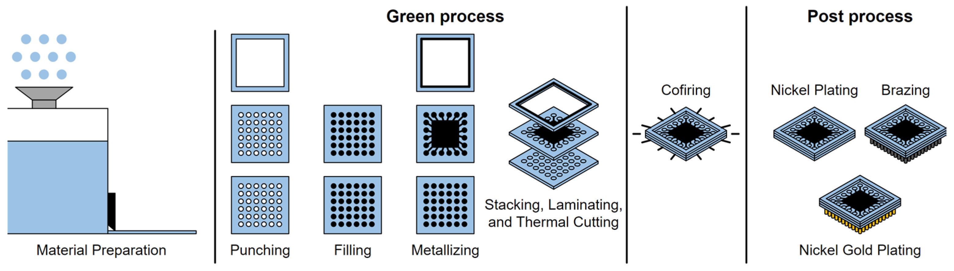
2. Multi-Material 3D Printing Methods
2.1. Material Jetting (MJ)
|
Types of Functional Inks |
Printing Methods |
Applications |
Electrical Properties |
|---|---|---|---|
|
Metal nanoparticles (MNPs) inks |
0.08–4.74 Ω sq−1 after 1 h of thermal sintering at 150 °C [29]; 0.4 Ω sq−1 after 30 min of thermal sintering at 250 °C [27] |
||
|
Non-enzymatic electrochemical sensors [30]; micro-hotplates [31] |
0.06 Ω cm−1 after 30 min thermal sintering at 100 °C [30]; 8.7 ± 2.5 μΩ cm after 1 h of thermal sintering at 120 °C followed by 250 °C for 4 h [31] |
||
|
Conductive patterns and tracks [32]; micro-electronic devices [33] |
6.18 Ω sq−1 after applying 5454 J energy [32]; 9.20 µΩ cm after 1 h of thermal sintering at 230 °C in inert atmosphere [33] |
||
|
~102 S cm−1 [34]; 22.32 S cm−1 was achieved after 2 ms of sintering by 1 flash with energy of 25.88 J/cm2, and the final conductivity of 34.72 S cm−1 was achieved by an optimum laser power [35] |
|||
|
Conductive polymer inks |
0.02 S cm−1 after 20 min of thermal annealing at 120 °C (120 nm thick) [36]; 0.323 ± 0.075 S cm−1 [37] |
||
|
BBL: PEI inks; Spray-coating [38] |
Organic electrochemical transistors and bioelectronics [38] |
8 S cm−1 after 2 h of thermal annealing at 140 °C inside a nitrogen-filled glovebox [38] |
|
|
Ceramic nanoparticle (CNP) inks |
Al2O3 CNPs inks; IJP [39] |
Thin film radio-frequency capacitors [39] |
The dielectric constant of the printed alumina layer (~120 nm thick with ~0.5 nm RMS surface roughness after the thermal annealing at 400 °C) was 6.2 [39] |
|
Piezoelectric generators [40]; interdigitated capacitors [41] |
The piezoelectric generator had an open-circuit voltage of ~7 V, a current density of 0.21 μA·cm−2, and a power density of 0.42 μW·cm−2 [40]; the dielectric constant was 7 [41] |
||
|
/ |
|||
|
Dielectric layers for flexible electronics [44]; resistive switches [45] |
The ZrO2 dielectric film (dielectric constant of 10) afforded a leakage current density of 5.4 × 10⁻⁶ A/cm2 at 1 MV/cm [44]. The printed resistive switch showed stable bipolar memristive switching behavior around ± 3 V [45] |
||
|
Mesoporous TiO2 electron transport layers for perovskite solar cells [46]; dielectric layers [47] |
The perovskite solar cell had a power conversion efficiency of 18.29% [46]; the current-voltage characteristics of conducting oxide-TiO2-Ag devices showed diode behavior [47] |
||
|
Ba0.6Sr0.4TiO3 CNPs inks; IJP [48] |
Dielectric layers for capacitors [48] |
The relative dielectric constant was 28 ± 1.7, and the dielectric loss was 0.043 ± 0.006 (at 10 kHz) [48] |
|
|
Ca2Nb3O10 CNPs inks; AJP [49] |
Thin-film transistors [49] |
The films deposited by Ca2Nb3O10 ink with a mass fraction of 82 wt% showed a dielectric constant of 8.5 and a dielectric loss of 0.058 (at 1 MHz) [49] |
|
|
Glass silicate CNPs inks; IJP [50] |
Multilayer hybrid circuits [50] |
/ |
|
|
Dielectric polymer inks |
Polyimide (PI) inks; IJP [51] |
Capacitors for microelectronic devices [51] |
The printed capacitor with 25 ± 0.2 µm thick PI layer showed a capacitance value of 103 pF [51] |
|
Poly 4-vinylphenol (PVP) inks; IJP [52] |
Flexible capacitors for wearable electronics [52] |
The printed capacitor with 4.5 µm thick PVP layer showed a capacitance value of 163 pF [52] |
|
|
Polyvinyl alcohol (PVA) inks; EHD [53] |
Gate insulators in organic field-effect transistors [53] |
The organic field-effect transistors with PVA-based gate insulators show stable operation with low gate leakage currents [53] |
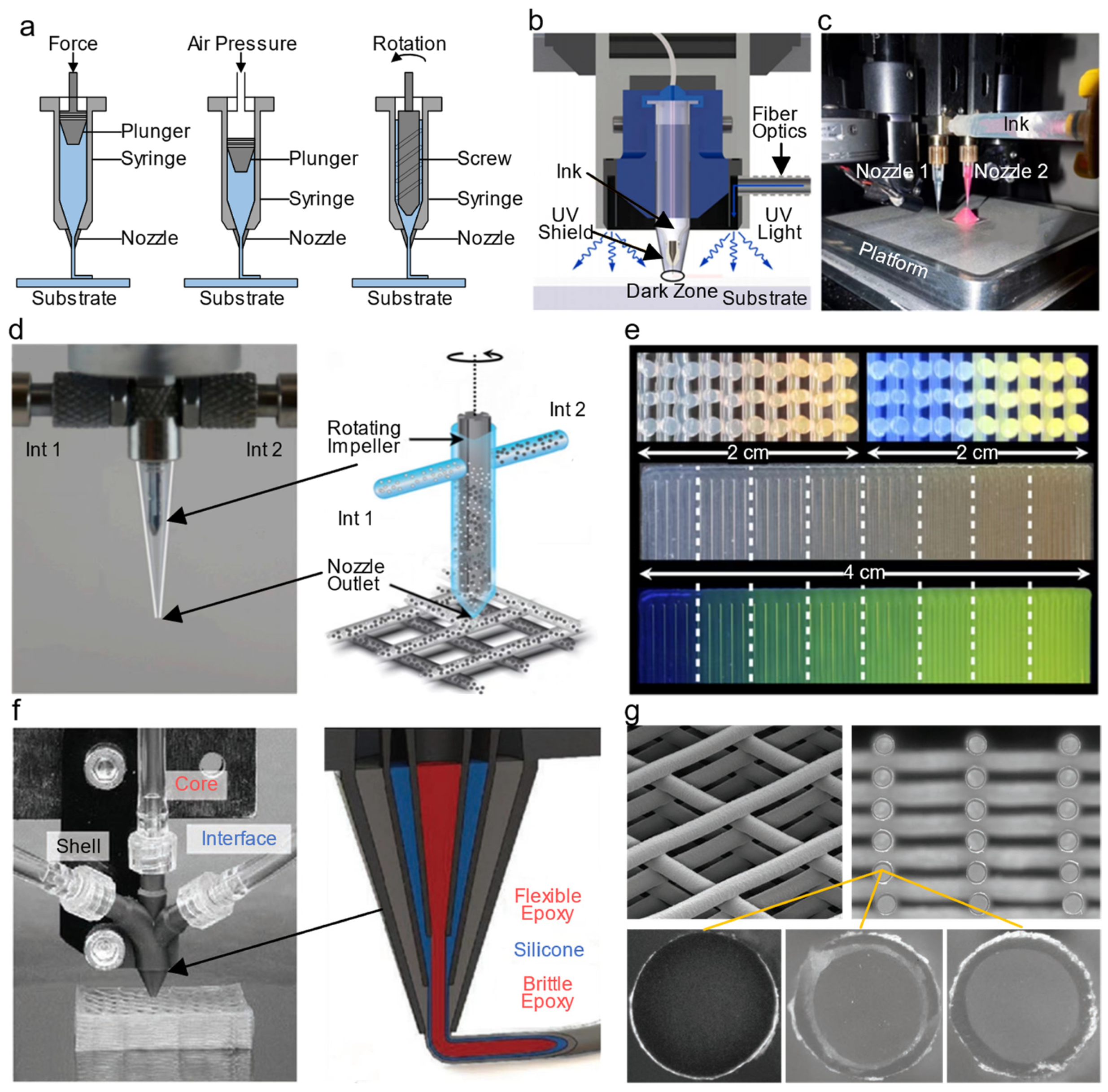
2.2. Direct Ink Writing (DIW)
2.3. Fused Deposition Modeling (FDM)
2.4. Vat Photopolymerization (VP)

3. Applications of Multi-Material 3D Printing in Functional Ceramic Devices
|
Compositions |
Multi-Material 3D Printing Techniques |
Applications |
Properties |
Ref. |
|---|---|---|---|---|
|
Dielectric material (ink): Ca2NaNb4O13 + Isopropanol + 2-butyl alcohol Electrode material (ink): Ag |
IJP |
Capacitors |
The capacitor showed a capacitance density of ≈210 pF/mm2 |
[120] |
|
Dielectric material (ink): Ba0.6Sr0.4TiO3-ZnO-B2O3 + Butyl diglycol + isopropyl alcohol + ethyl cellulose Electrode material (ink): Ag |
IJP |
Varactors |
The varactors showed a tunability between 14.4% and 16.4% under a tuning field of 5 V/µm |
[121] |
|
Dielectric material (ink): MgTiO3 Electrode material (ink): Ag |
IJP |
Capacitors |
/ |
[122] |
|
Dielectric material (ink): Pb0.97La0.02Zr0.53Ti0.47O3 + ethylene glycol + ethanolamine Electrode material (ink): Ag |
IJP |
Capacitors |
/ |
[123] |
|
Dielectric material (ink): Ba0.6Sr0.4TiO3 + Poly (ethylene glycol) diacrylate Electrode material (ink): Ag |
IJP |
Multilayer ceramic capacitors |
The multilayer ceramic capacitors showed a capacitance density of ≈ 500 pF/mm2 |
[124] |
|
Dielectric material (ink): BaO-Al2O3-SiO2-MnO-TiO2 Electrode material (ink): Cu |
IJP |
Multilayer ceramic substrates |
The multilayer ceramic substrate showed a shrinkage ratio of ≈15% |
[125] |
|
Dielectric material (ink): BaTiO3 Electrode material (/): Cu |
AJP + etching + sputtering + plating |
Multilayer ceramic substrates |
The multilayer ceramic substrate showed a permittivity of ≈ 3000 and a dielectric loss of ≈ 7% at 1 MHz |
[126] |
|
Dielectric material (slurry): Al2O3 Electrode material (slurry): tungsten |
SLA + DIW |
Multilayer ceramic substrates |
The multilayer ceramic substrates showed a Young modulus E of ≈ 280 ± 11 GPa |
[127] |
|
Dielectric material (ink): ZrO2 Electrode material (ink): Ag |
IJP + AJP |
Microstrip antennas |
The bulk ZrO2 showed a relative permittivity of 23 and a loss tangent of 0.0013 at microwave frequencies |
[128] |
|
Dielectric material (ink): SiO2 + hexanediol diacrylate (HDDA) + alkyl-diphenyl oxide disulfonate Electrode material (ink): Cu |
IJP |
Microstrip antennas |
The resistance was 2.43 × 10¹³ Ω·cm (174.3 µm thick dielectric layer) |
[129] |
|
Dielectric material (filament): TiO2 + cyclo-olefin polymer (COP) Electrode material (slurry): Ag |
FDM + DIW |
Microstrip antennas |
The 30% loaded COP-TiO2 showed a relative permittivity of 4.56 and a loss tangent of 0.0016 after sintering at 1100 °C |
[130] |
|
Dielectric material (filament): NdTi03 + polydimethylsiloxane (PDMS) Electrode material (slurry): Ag |
FDM + DIW |
Microstrip antennas |
The 25% loaded PDMS-NdTiO3 showed a permittivity of 9.22 and a loss tangent of 0.025 at frequencies up to 17 GHz |
[131] |
|
Dielectric material (filament): MgCaTi02 + PDMS Electrode material (slurry): Ag |
FDM + DIW |
Microstrip antennas |
The 19.6 GHz microstrip antenna showed a return loss of 20 dB along with a 10% bandwidth |
[132] |
References
- Yin, Q.; Zhu, B.; Zeng, H. Microstructure, Property and Processing of Functional Ceramics; Springer Science & Business Media: Berlin, Germany, 2010; pp. 1–6.
- Ruiz-Morales, J.; Tarancón, A.; Canales-Vázquez, J.; Méndez-Ramos, J.; Hernández-Afonso, L.; Acosta-Mora, P.; Rueda, J.R.M.; Fernández-González, R. Three dimensional printing of components and functional devices for energy and environmental applications. Energy Environ. Sci. 2017, 10, 846–859.
- Pan, M.-J.; Randall, C.A. A brief introduction to ceramic capacitors. IEEE Electr. Insul. Mag. 2010, 26, 44–50.
- Thelemann, T.; Bartnitzek, T.; Suphan, K.-H.; Apel, S. Advancing packaging solutions using 3D capabilities of ceramic multilayers. In Proceedings of the 2015 European Microelectronics Packaging Conference (EMPC), Friedrichshafen, Germany, 14–16 September 2015; pp. 1–6.
- Oshima, S.; Wada, K.; Murata, R.; Shimakata, Y. Multilayer Dual-Band Bandpass Filter in Low-Temperature Co-Fired Ceramic Substrate for Ultra-Wideband Applications. IEEE Trans. Microw. Theory Tech. 2010, 58, 614–623.
- Liu, Z.; Wang, P.; Zeng, Z. Enhancement of the Gain for Microstrip Antennas Using Negative Permeability Metamaterial on Low Temperature Co-Fired Ceramic (LTCC) Substrate. IEEE Antennas Wirel. Propag. Lett. 2013, 12, 429–432.
- Chen, H.; Che, W.; Wang, X.; Feng, W. Size-Reduced Planar and Nonplanar SIW Gysel Power Divider Based on Low Temperature Co-fired Ceramic Technology. IEEE Microw. Wirel. Compon. Lett. 2017, 27, 1065–1067.
- Bhutani, A.; Gottel, B.; Lipp, A.; Zwick, T. Packaging Solution Based on Low-Temperature Cofired Ceramic Technology for Frequencies Beyond 100 GHz. IEEE Trans. Compon. Packag. Manuf. Technol. 2018, 9, 945–954.
- Ren, L.; Luo, X.; Zhou, H. The tape casting process for manufacturing low-temperature co-fired ceramic green sheets: A review. J. Am. Ceram. Soc. 2018, 101, 3874–3889.
- ISO/ASTM 52900:2015; Additive Manufacturing: General: Principles: Terminology. ISO: Geneva, Switzerland, 2015; pp. 1–19.
- Wolf, A.; Rosendahl, P.L.; Knaack, U. Additive manufacturing of clay and ceramic building components. Autom. Constr. 2021, 133, 103956.
- He, Q.; Jiang, J.; Yang, X.; Zhang, L.; Zhou, Z.; Zhong, Y.; Shen, Z. Additive manufacturing of dense zirconia ceramics by fused deposition modeling via screw extrusion. J. Eur. Ceram. Soc. 2020, 41, 1033–1040.
- Wang, F.; Li, Z.; Lou, Y.; Zeng, F.; Hao, M.; Lei, W.; Wang, X.; Wang, X.; Fan, G.; Lu, W. Stereolithographic additive manufacturing of Luneburg lens using Al2O3-based low sintering temperature ceramics for 5G MIMO antenna. Addit. Manuf. 2021, 47, 102244.
- Liu, K.; Zhou, C.; Hu, J.; Zhang, S.; Zhang, Q.; Sun, C.; Shi, Y.; Sun, H.; Yin, C.; Zhang, Y.; et al. Fabrication of barium titanate ceramics via digital light processing 3D printing by using high refractive index monomer. J. Eur. Ceram. Soc. 2021, 41, 5909–5917.
- Xing, H.; Zou, B.; Liu, X.; Wang, X.; Huang, C.; Hu, Y. Fabrication strategy of complicated Al2O3-Si3N4 functionally graded materials by stereolithography 3D printing. J. Eur. Ceram. Soc. 2020, 40, 5797–5809.
- Khatri, B.; Lappe, K.; Habedank, M.; Mueller, T.; Megnin, C.; Hanemann, T. Fused Deposition Modeling of ABS-Barium Titanate Composites: A Simple Route towards Tailored Dielectric Devices. Polymers 2018, 10, 666.
- Lee, J.-H.; Kim, J.-H.; Hwang, K.-T.; Hwang, H.-J.; Han, K.-S. Digital inkjet printing in three dimensions with multiple ceramic compositions. J. Eur. Ceram. Soc. 2020, 41, 1490–1497.
- Gong, P.; Li, Y.; Xin, C.; Chen, Q.; Hao, L.; Sun, Q.; Li, Z. Multimaterial 3D-printing barium titanate/carbonyl iron composites with bilayer-gradient honeycomb structure for adjustable broadband microwave absorption. Ceram. Int. 2021, 48, 9873–9881.
- Smay, J.E.; Nadkarni, S.S.; Xu, J. Direct Writing of Dielectric Ceramics and Base Metal Electrodes. Int. J. Appl. Ceram. Technol. 2007, 4, 47–52.
- Castrejon-Pita, J.R.; Baxter, W.; Morgan, J.; Temple, S.; Martin, G.; Hutchings, I.M. Future, opportunities and challenges of inkjet technologies. At. Sprays 2013, 23, 541–565.
- Dilag, J.; Chen, T.; Li, S.; Bateman, S.A. Design and direct additive manufacturing of three-dimensional surface micro-structures using material jetting technologies. Addit. Manuf. 2019, 27, 167–174.
- Choi, K.-H.; Yoo, J.; Lee, C.K.; Lee, S.-Y. All-inkjet-printed, solid-state flexible supercapacitors on paper. Energy Environ. Sci. 2016, 9, 2812–2821.
- Craton, M.T.; Sorocki, J.; Piekarz, I.; Gruszczynski, S.; Wincza, K.; Papapolymerou, J. Realization of fully 3D printed W-band bandpass filters using aerosol jet printing technology. In Proceedings of the 2018 48th European Microwave Conference (EuMC), Madrid, Spain, 25–27 September 2018; pp. 1013–1016.
- Theiler, P.M.; Lütolf, F.; Ferrini, R. Non-contact printing of optical waveguides using capillary bridges. Opt. Express 2018, 26, 11934–11939.
- Eggenhuisen, T.M.; Galagan, Y.; Biezemans, A.F.K.V.; Slaats, T.M.W.L.; Voorthuijzen, W.P.; Kommeren, S.; Shanmugam, S.; Teunissen, J.P.; Hadipour, A.; Verhees, W.J.H.; et al. High efficiency, fully inkjet printed organic solar cells with freedom of design. J. Mater. Chem. A 2015, 3, 7255–7262.
- Qin, H.; Dong, J.; Lee, Y.-S. Fabrication and electrical characterization of multi-layer capacitive touch sensors on flexible substrates by additive e-jet printing. J. Manuf. Process. 2017, 28, 479–485.
- Khan, A.; Rahman, K.; Ali, S.; Khan, S.; Wang, B.; Bermak, A. Fabrication of circuits by multi-nozzle electrohydrodynamic inkjet printing for soft wearable electronics. J. Mater. Res. 2021, 36, 3568–3578.
- Laurila, M.-M.; Khorramdel, B.; Mantysalo, M. Combination of E-Jet and Inkjet Printing for Additive Fabrication of Multilayer High-Density RDL of Silicon Interposer. IEEE Trans. Electron Devices 2017, 64, 1217–1224.
- Karim, N.; Afroj, S.; Tan, S.; Novoselov, K.S.; Yeates, S.G. All Inkjet-Printed Graphene-Silver Composite Ink on Textiles for Highly Conductive Wearable Electronics Applications. Sci. Rep. 2019, 9, 8035.
- Kant, T.; Shrivas, K.; Tapadia, K.; Devi, R.; Ganesan, V.; Deb, M.K. Inkjet-printed paper-based electrochemical sensor with gold nano-ink for detection of glucose in blood serum. New J. Chem. 2021, 45, 8297–8305.
- Khan, S.; Nguyen, T.; Lubej, M.; Thiery, L.; Vairac, P.; Briand, D. Low-power printed micro-hotplates through aerosol jetting of gold on thin polyimide membranes. Microelectron. Eng. 2018, 194, 71–78.
- Lim, S.; Joyce, M.; Fleming, P.D.; Aijazi, A.T.; Atashbar, M. Inkjet Printing and Sintering of Nano-Copper Ink. J. Imaging Sci. Technol. 2013, 57, 50506-1–50506-7.
- Khan, A.; Rahman, K.; Kim, D.S.; Choi, K.H. Direct printing of copper conductive micro-tracks by multi-nozzle electrohydrodynamic inkjet printing process. J. Mater. Process. Technol. 2011, 212, 700–706.
- Majee, S.; Karlsson, M.C.F.; Wojcik, P.J.; Sawatdee, A.; Mulla, M.Y.; Alvi, N.U.H.; Dyreklev, P.; Beni, V.; Nilsson, D. Low temperature chemical sintering of inkjet-printed Zn nanoparticles for highly conductive flexible electronic components. npj Flex. Electron. 2021, 5, 32.
- Mahajan, B.K.; Ludwig, B.; Shou, W.; Yu, X.; Fregene, E.; Xu, H.; Pan, H.; Huang, X. Aerosol printing and photonic sintering of bioresorbable zinc nanoparticle ink for transient electronics manufacturing. Sci. China Inf. Sci. 2018, 61, 060412.
- Singh, A.; Katiyar, M.; Garg, A. Understanding the formation of PEDOT:PSS films by ink-jet printing for organic solar cell applications. RSC Adv. 2015, 5, 78677–78685.
- Zips, S.; Grob, L.; Rinklin, P.; Terkan, K.; Adly, N.Y.; Weiß, L.J.K.; Mayer, D.; Wolfrum, B. Fully Printed μ-Needle Electrode Array from Conductive Polymer Ink for Bioelectronic Applications. ACS Appl. Mater. Interfaces 2019, 11, 32778–32786.
- Yang, C.-Y.; Stoeckel, M.-A.; Ruoko, T.-P.; Wu, H.-Y.; Liu, X.; Kolhe, N.B.; Wu, Z.; Puttisong, Y.; Musumeci, C.; Massetti, M.; et al. A high-conductivity n-type polymeric ink for printed electronics. Nat. Commun. 2021, 12, 2354.
- McKerricher, G.; Maller, R.; Mohammad, V.; McLachlan, M.A.; Shamim, A. Inkjet-printed thin film radio-frequency capacitors based on sol-gel derived alumina dielectric ink. Ceram. Int. 2017, 43, 9846–9853.
- Lim, J.; Jung, H.; Baek, C.; Hwang, G.-T.; Ryu, J.; Yoon, D.; Yoo, J.; Park, K.-I.; Kim, J.H. All-inkjet-printed flexible piezoelectric generator made of solvent evaporation assisted BaTiO3 hybrid material. Nano Energy 2017, 41, 337–343.
- Craton, M.T.; He, Y.; Roch, A.; Chahal, P.; Papapolymerou, J. Additively manufactured interdigitated capacitors using barium titanate nanocomposite inks. In Proceedings of the 2019 49th European Microwave Conference (EuMC), Paris, France, 1–3 October 2019; pp. 488–491.
- Rahul, S.; Balasubramanian, K.; Venkatesh, S. Optimizing inkjet printing process to fabricate thick ceramic coatings. Ceram. Int. 2017, 43, 4513–4519.
- Özkol, E.; Wätjen, A.M.; Bermejo, R.; Deluca, M.; Ebert, J.; Danzer, R.; Telle, R. Mechanical characterisation of miniaturised direct inkjet printed 3Y-TZP specimens for microelectronic applications. J. Eur. Ceram. Soc. 2010, 30, 3145–3152.
- Zhu, Z.; Zhang, J.; Zhou, Z.; Ning, H.; Cai, W.; Wei, J.; Zhou, S.; Yao, R.; Lu, X.; Peng, J. A Simple, Low Cost Ink System for Drop-on-Demand Printing High Performance Metal Oxide Dielectric Film at Low Temperature. ACS Appl. Mater. Interfaces 2019, 11, 5193–5199.
- Awais, M.N.; Kim, H.C.; Doh, Y.H.; Choi, K.H. ZrO2 flexible printed resistive (memristive) switch through electrohydrodynamic printing process. Thin Solid Films 2013, 536, 308–312.
- Huckaba, A.J.; Lee, Y.; Xia, R.; Paek, S.; Bassetto, V.C.; Oveisi, E.; Lesch, A.; Kinge, S.; Dyson, P.J.; Girault, H.; et al. Inkjet-Printed Mesoporous TiO2 and Perovskite Layers for High Efficiency Perovskite Solar Cells. Energy Technol. 2018, 7, 317–324.
- Padrón-Hernández, W.; Ceballos-Chuc, M.C.; Pourjafari, D.; Oskam, G.; Tinoco, J.C.; Martínez-López, A.; Rodríguez-Gattorno, G. Stable inks for inkjet printing of TiO2 thin films. Mater. Sci. Semicond. Process. 2018, 81, 75–81.
- Mikolajek, M.; Friederich, A.; Kohler, C.; Rosen, M.; Rathjen, A.; Krüger, K.; Binder, J.R. Direct Inkjet Printing of Dielectric Ceramic/Polymer Composite Thick Films. Adv. Eng. Mater. 2015, 17, 1294–1301.
- Wu, X.; Fei, F.; Chen, Z.; Su, W.; Cui, Z. A new nanocomposite dielectric ink and its application in printed thin-film transistors. Compos. Sci. Technol. 2014, 94, 117–122.
- Singlard, M.; Aimable, A.; Lejeune, M.; Dossou-Yovo, C.; Poncelet, M.; Noguera, R.; Modes, C. Aqueous suspensions of glass silicate dielectric powders for ink-jet printing applications. Powder Technol. 2014, 266, 303–311.
- Zhang, F.; Tuck, C.; Hague, R.; He, Y.; Saleh, E.; Li, Y.; Sturgess, C.; Wildman, R. Inkjet printing of polyimide insulators for the 3D printing of dielectric materials for microelectronic applications. J. Appl. Polym. Sci. 2016, 133, 43361–43371.
- Yi, L.; Torah, R.; Beeby, S.; Tudor, J. An all-inkjet printed flexible capacitor on a textile using a new poly(4-vinylphenol) dielectric ink for wearable applications. In Proceedings of the Sensors, Taipei, Taiwan, 28–31 October 2012.
- Jung, C.; Tang, X.; Kwon, H.-J.; Wang, R.; Oh, S.M.; Ye, H.; Jeong, Y.R.; Jeong, Y.J.; Kim, S.H. Electrohydrodynamic-Printed Polyvinyl Alcohol-Based Gate Insulators for Organic Integrated Devices. Adv. Eng. Mater. 2022, 24, 2100900.
- Holness, F.B.; Price, A.D. Direct ink writing of 3D conductive polyaniline structures and rheological modelling. Smart Mater. Struct. 2017, 27, 015006.
- Gu, S.; Tian, Y.; Liang, K.; Ji, Y. Chitin nanocrystals assisted 3D printing of polycitrate thermoset bioelastomers. Carbohydr. Polym. 2021, 256, 117549.
- Wang, P.; Li, J.; Wang, G.; He, L.; Yu, Y.; Xu, B. Multimaterial Additive Manufacturing of LTCC Matrix and Silver Conductors for 3D Ceramic Electronics. Adv. Mater. Technol. 2022, 7, 2101462.
- Jiang, Q.; Yang, D.; Yuan, H.; Wang, R.; Hao, M.; Ren, W.; Shao, G.; Wang, H.; Cui, J.; Hu, J. Fabrication and properties of Si2N2O-Si3N4 ceramics via direct ink writing and low-temperature sintering. Ceram. Int. 2021, 48, 32–41.
- Xu, C.; Quinn, B.; Lebel, L.L.; Therriault, D.; L’Espérance, G. Multi-material direct ink writing (DIW) for complex 3D metallic structures with removable supports. ACS Appl. Mater. Interfaces 2019, 11, 8499–8506.
- Li, Z.; Li, Y.; Shi, B.; Tang, D.; Wang, Y.; Hao, L. Dual gradient direct ink writing of functional geopolymer-based carbonyl-iron/graphene composites for adjustable broadband microwave absorption. Ceram. Int. 2022, 48, 9277–9285.
- Luo, B.; Wei, Y.; Chen, H.; Zhu, Z.; Fan, P.; Xu, X.; Xie, B. Printing Carbon Nanotube-Embedded Silicone Elastomers via Direct Writing. ACS Appl. Mater. Interfaces 2018, 10, 44796–44802.
- Cheng, M.; Ramasubramanian, A.; Rasul, G.; Jiang, Y.; Yuan, Y.; Foroozan, T.; Deivanayagam, R.; Saray, M.T.; Rojaee, R.; Song, B.; et al. Direct Ink Writing of Polymer Composite Electrolytes with Enhanced Thermal Conductivities. Adv. Funct. Mater. 2021, 31, 2006683.
- Lewis, J.A. Direct ink writing of 3D functional materials. Adv. Funct. Mater. 2006, 16, 2193–2204.
- Tu, R.; Sodano, H.A. Additive manufacturing of high-performance vinyl ester resin via direct ink writing with UV-thermal dual curing. Addit. Manuf. 2021, 46, 102180.
- Li, L.; Lin, Q.; Tang, M.; Duncan, A.J.; Ke, C. Advanced polymer designs for direct-ink-write 3D printing. Chemistry 2019, 25, 10768–10781.
- Ober, T.J.; Foresti, D.; Lewis, J.A. Active mixing of complex fluids at the microscale. Proc. Natl. Acad. Sci. USA 2015, 112, 12293–12298.
- Mueller, J.; Raney, J.R.; Shea, K.; Lewis, J.A. Architected Lattices with High Stiffness and Toughness via Multicore–Shell 3D Printing. Adv. Mater. 2018, 30, e1705001.
- Ahammed, S.R.; Praveen, A.S. Optimization parameters effects on electrical conductivity of 3D printed circuits fabricated by direct ink writing method using functionalized multiwalled carbon nanotubes and polyvinyl alcohol conductive ink. Int. J. Simul. Multidiscip. Des. Optim. 2021, 12, 7.
- Udofia, E.N.; Zhou, W. Microextrusion based 3D printing—A review. In Proceedings of the 2018 International Solid Freeform Fabrication Symposium, Austin, TX, USA, 13–15 August 2018.
- Xu, M.; Lewis, J.A. Phase Behavior and Rheological Properties of Polyamine-Rich Complexes for Direct-Write Assembly. Langmuir 2007, 23, 12752–12759.
- Sun, K.; Wei, T.-S.; Ahn, B.Y.; Seo, J.Y.; Dillon, S.J.; Lewis, J.A. 3D Printing of Interdigitated Li-Ion Microbattery Architectures. Adv. Mater. 2013, 25, 4539–4543.
- Han, D.; Lee, H. Recent advances in multi-material additive manufacturing: Methods and applications. Curr. Opin. Chem. Eng. 2020, 28, 158–166.
- Golobic, A.M.; Durban, M.D.; Fisher, S.E.; Grapes, M.; Ortega, J.M.; Spadaccini, C.M.; Duoss, E.B.; Gash, A.E.; Sullivan, K.T. Active Mixing of Reactive Materials for 3D Printing. Adv. Eng. Mater. 2019, 21, 1900147.
- Hassan, I.; Selvaganapathy, P.R. A microfluidic printhead with integrated hybrid mixing by sequential injection for multimaterial 3D printing. Addit. Manuf. 2022, 50, 102559.
- Pack, R.C.; Romberg, S.K.; Badran, A.A.; Hmeidat, N.S.; Yount, T.; Compton, B.G. Carbon Fiber and Syntactic Foam Hybrid Materials via Core–Shell Material Extrusion Additive Manufacturing. Adv. Mater. Technol. 2020, 5, 2000731.
- Chen, K.; Zhang, L.; Kuang, X.; Li, V.; Lei, M.; Kang, G.; Wang, Z.L.; Qi, H.J. Dynamic Photomask-Assisted Direct Ink Writing Multimaterial for Multilevel Triboelectric Nanogenerator. Adv. Funct. Mater. 2019, 29, 1903568.
- Kim, S.; Oh, J.; Jeong, D.; Park, W.; Bae, J. Consistent and Reproducible Direct Ink Writing of Eutectic Gallium–Indium for High-Quality Soft Sensors. Soft Robot. 2018, 5, 601–612.
- Chen, B.; Jiang, Y.; Tang, X.; Pan, Y.; Hu, S. Fully Packaged Carbon Nanotube Supercapacitors by Direct Ink Writing on Flexible Substrates. ACS Appl. Mater. Interfaces 2017, 9, 28433–28440.
- Jiang, Y.; Cheng, M.; Shahbazian-Yassar, R.; Pan, Y. Direct Ink Writing of Wearable Thermoresponsive Supercapacitors with rGO/CNT Composite Electrodes. Adv. Mater. Technol. 2019, 4, 1900691.
- Park, S.H.; Su, R.; Jeong, J.; Guo, S.; Qiu, K.; Joung, D.; Meng, F.; McAlpine, M.C. 3D Printed Polymer Photodetectors. Adv. Mater. 2018, 30, e1803980.
- Hinton, J.; Mirgkizoudi, M.; Campos-Zatarain, A.; Flynn, D.; Harris, R.; Kay, R. Digitally-driven hybrid manufacture of ceramic thick-film substrates. In Proceedings of the 2018 7th Electronic System-Integration Technology Conference (ESTC), Dresden, Germany, 18–21 September 2018; pp. 1–5.
- Sears, N.; Dhavalikar, P.; Whitely, M.; Cosgriff-Hernandez, E. Fabrication of biomimetic bone grafts with multi-material 3D printing. Biofabrication 2017, 9, 025020.
- Basu, B. Natural bone and tooth: Structure and properties. In Biomaterials for Musculoskeletal Regeneration; Springer: Berlin/Heidelberg, Germany, 2017; pp. 45–85.
- Wang, Q.; Xu, J.; Jin, H.; Zheng, W.; Zhang, X.; Huang, Y.; Qian, Z. Artificial periosteum in bone defect repair—A review. Chin. Chem. Lett. 2017, 28, 1801–1807.
- Li, X.; Yuan, Y.; Liu, L.; Leung, Y.-S.; Chen, Y.; Guo, Y.; Chai, Y.; Chen, Y. 3D printing of hydroxyapatite/tricalcium phosphate scaffold with hierarchical porous structure for bone regeneration. Bio-Design Manuf. 2020, 3, 15–29.
- Betancourt, N.; Chen, X. Review of extrusion-based multi-material bioprinting processes. Bioprinting 2022, 25, e00189.
- Poltue, T.; Karuna, C.; Khrueaduangkham, S.; Seehanam, S.; Promoppatum, P. Design exploration of 3D-printed triply periodic minimal surface scaffolds for bone implants. Int. J. Mech. Sci. 2021, 211, 106762.
- Boparai, K.S.; Singh, R.; Singh, H. Development of rapid tooling using fused deposition modeling: A review. Rapid Prototyp. J. 2016, 22, 281–299.
- Ryder, M.A.; Lados, D.A.; Iannacchione, G.S.; Peterson, A.M. Fabrication and properties of novel polymer-metal composites using fused deposition modeling. Compos. Sci. Technol. 2018, 158, 43–50.
- Hwang, S.; Reyes, E.I.; Moon, K.-S.; Rumpf, R.C.; Kim, N.S. Thermo-mechanical Characterization of Metal/Polymer Composite Filaments and Printing Parameter Study for Fused Deposition Modeling in the 3D Printing Process. J. Electron. Mater. 2014, 44, 771–777.
- Castles, F.; Isakov, D.; Lui, A.; Lei, Q.; Dancer, C.; Wang, Y.; Janurudin, J.; Speller, S.; Grovenor, C.; Grant, P.S. Microwave dielectric characterisation of 3D-printed BaTiO3/ABS polymer composites. Sci. Rep. 2016, 6, 22714.
- Wu, Y.; Isakov, D.; Grant, P.S. Fabrication of Composite Filaments with High Dielectric Permittivity for Fused Deposition 3D Printing. Materials 2017, 10, 1218.
- Castro, J.D.D. Engineered Nanocomposite Materials for Microwave/Millimeter-Wave Applications of Fused Deposition Modeling. Ph.D. Thesis, University of South Florida, Fowler Avenue Tampa, FL, USA, 2017.
- Goulas, A.; McGhee, J.R.; Whittaker, T.; Ossai, D.; Mistry, E.; Whittow, W.; Vaidhyanathan, B.; Reaney, I.M.; Vardaxoglou, J.Y.C.; Engstrøm, D.S. Synthesis and dielectric characterisation of a low loss BaSrTiO3/ABS ceramic/polymer composite for fused filament fabrication additive manufacturing. Addit. Manuf. 2022, 55, 102844.
- Wang, P.; Zou, B.; Ding, S.; Huang, C.; Shi, Z.; Ma, Y.; Yao, P. Preparation of short CF/GF reinforced PEEK composite filaments and their comprehensive properties evaluation for FDM-3D printing. Compos. Part B Eng. 2020, 198, 108175.
- Heidari-Rarani, M.; Rafiee-Afarani, M.; Zahedi, A. Mechanical characterization of FDM 3D printing of continuous carbon fiber reinforced PLA composites. Compos. Part B Eng. 2019, 175, 107147.
- Distler, T.; Fournier, N.; Grünewald, A.; Polley, C.; Seitz, H.; Detsch, R.; Boccaccini, A.R. Polymer-Bioactive Glass Composite Filaments for 3D Scaffold Manufacturing by Fused Deposition Modeling: Fabrication and Characterization. Front. Bioeng. Biotechnol. 2020, 8, 552.
- Parulski, C.; Jennotte, O.; Lechanteur, A.; Evrard, B. Challenges of fused deposition modeling 3D printing in pharmaceutical applications: Where are we now? Adv. Drug Deliv. Rev. 2021, 175, 113810.
- Mohamed, O.A.; Masood, S.; Bhowmik, J.L. Optimization of fused deposition modeling process parameters: A review of current research and future prospects. Adv. Manuf. 2015, 3, 42–53.
- Abel, J.; Scheithauer, U.; Janics, T.; Hampel, S.; Cano, S.; Müller-Köhn, A.; Günther, A.; Kukla, C.; Moritz, T. Fused Filament Fabrication (FFF) of Metal-Ceramic Components. J. Vis. Exp. 2019, 143, e57693.
- Pagac, M.; Hajnys, J.; Ma, Q.-P.; Jancar, L.; Jansa, J.; Stefek, P.; Mesicek, J. A Review of Vat Photopolymerization Technology: Materials, Applications, Challenges, and Future Trends of 3D Printing. Polymers 2021, 13, 598.
- Lemma, E.D.; Spagnolo, B.; De Vittorio, M.; Pisanello, F. Studying Cell Mechanobiology in 3D: The Two-Photon Lithography Approach. Trends Biotechnol. 2019, 37, 358–372.
- Sänger, J.C.; Pauw, B.R.; Sturm, H.; Günster, J. First time additively manufactured advanced ceramics by using two-photon polymerization for powder processing. Open Ceram. 2020, 4, 100040.
- Lambert, P.M.; Campaigne III, E.A.; Williams, C.B. Design considerations for mask projection microstereolithography systems. In Proceedings of the 2013 International Solid Freeform Fabrication Symposium, 2013; Available online: https://repositories.lib.utexas.edu/handle/2152/88484 (accessed on 21 September 2022).
- Huang, J.; Qin, Q.; Wang, J. A Review of Stereolithography: Processes and Systems. Processes 2020, 8, 1138.
- Männel, M.; Baysak, E.; Thiele, J. Fabrication of Microfluidic Devices for Emulsion Formation by Microstereolithography. Molecules 2021, 26, 2817.
- Zhao, W.; Wang, Z.; Zhang, J.; Wang, X.; Xu, Y.; Ding, N.; Peng, Z. Vat Photopolymerization 3D Printing of Advanced Soft Sensors and Actuators: From Architecture to Function. Adv. Mater. Technol. 2021, 6, 2001218.
- Lopes, A.J.; MacDonald, E.; Wicker, R.B. Integrating stereolithography and direct print technologies for 3D structural electronics fabrication. Rapid Prototyp. J. 2012, 18, 129–143.
- Peng, X.; Kuang, X.; Roach, D.J.; Wang, Y.; Hamel, C.M.; Lu, C.; Qi, H.J. Integrating digital light processing with direct ink writing for hybrid 3D printing of functional structures and devices. Addit. Manuf. 2021, 40, 101911.
- Choi, J.-W.; MacDonald, E.; Wicker, R. Multi-material microstereolithography. Int. J. Adv. Manuf. Technol. 2010, 49, 543–551.
- Choi, J.-W.; Kim, H.-C.; Wicker, R. Multi-material stereolithography. J. Mater. Process. Technol. 2011, 211, 318–328.
- Ge, Q.; Sakhaei, A.H.; Lee, H.; Dunn, C.K.; Fang, N.X.; Dunn, M.L. Multimaterial 4D Printing with Tailorable Shape Memory Polymers. Sci. Rep. 2016, 6, 31110.
- Hohnholz, A.; Obata, K.; Albrecht, D.; Koch, J.; Hohenhoff, G.; Suttmann, O.; Kaierle, S.; Overmeyer, L. Multimaterial bathless stereolithography using aerosol jet printing and UV laser based polymerization. J. Laser Appl. 2019, 31, 022301.
- Kowsari, K.; Akbari, S.; Wang, D.; Fang, N.X.; Ge, Q. High-Efficiency High-Resolution Multimaterial Fabrication for Digital Light Processing-Based Three-Dimensional Printing. 3D Print. Addit. Manuf. 2018, 5, 185–193.
- Kang, S.; Chang, S.-Y.; Costa, A.; Kowsari, K.; Ma, A.W.K. Additive manufacturing of embedded carbon nanocomposite structures with multi-material digital light processing (MMDLP). J. Mater. Res. 2021, 36, 3558–3567.
- Grigoryan, B.; Sazer, D.W.; Avila, A.; Albritton, J.L.; Padhye, A.; Ta, A.H.; Greenfield, P.T.; Gibbons, D.L.; Miller, J.S. Development, characterization, and applications of multi-material stereolithography bioprinting. Sci. Rep. 2021, 11, 3171.
- Mao, H.; Jia, W.; Leung, Y.-S.; Jin, J.; Chen, Y. Multi-material stereolithography using curing-on-demand printheads. Rapid Prototyp. J. 2021, 27, 861–871.
- Chen, D.; Zheng, X. Multi-material Additive Manufacturing of Metamaterials with Giant, Tailorable Negative Poisson’s Ratios. Sci. Rep. 2018, 8, 9139.
- Miri, A.K.; Nieto, D.; Iglesias, L.; Goodarzi Hosseinabadi, H.; Maharjan, S.; Ruiz-Esparza, G.U.; Khoshakhlagh, P.; Manbachi, A.; Dokmeci, M.R.; Chen, S. Microfluidics-enabled multimaterial maskless stereolithographic bioprinting. Adv. Mater. 2018, 30, 1800242.
- Han, D.; Yang, C.; Fang, N.X.; Lee, H. Rapid multi-material 3D printing with projection micro-stereolithography using dynamic fluidic control. Addit. Manuf. 2019, 27, 606–615.
- Fu, Y.; Zhang, P.; Li, B.; Zhang, B.; Yu, Y.; Shen, Z.; Zhang, X.; Wu, J.; Nan, C.; Zhang, S. Inkjet Printing of Perovskite Nanosheets for Microcapacitors. Adv. Electron. Mater. 2021, 7, 2100402.
- Friederich, A.; Köhler, C.; Nikfalazar, M.; Wiens, A.; Jakoby, R.; Bauer, W.; Binder, J.R. Inkjet-Printed Metal-Insulator-Metal Capacitors for Tunable Microwave Applications. Int. J. Appl. Ceram. Technol. 2015, 12, E164–E173.
- Dossou-Yovo, C.; Mougenot, M.; Beaudrouet, E.; Bessaudou, M.; Bernardin, N.; Charifi, F.; Coquet, C.; Borella, M.; Noguera, R.; Modes, C.; et al. Inkjet Printing Technology: A Novel Bottom-up Approach for Multilayer Ceramic Components and High Definition Printed Electronic Devices. J. Microelectron. Electron. Packag. 2012, 9, 187–198.
- Matavž, A.; Benčan, A.; Kovač, J.; Chung, C.-C.; Jones, J.L.; Trolier-McKinstry, S.; Malič, B.; Bobnar, V. Additive Manufacturing of Ferroelectric-Oxide Thin-Film Multilayer Devices. ACS Appl. Mater. Interfaces 2019, 11, 45155–45160.
- Reinheimer, T.; Azmi, R.; Binder, J.R. Polymerizable Ceramic Ink System for Thin Inkjet-Printed Dielectric Layers. ACS Appl. Mater. Interfaces 2019, 12, 2974–2982.
- Hirao, T.; Hamada, S. Novel Multi-Material 3-Dimensional Low-Temperature Co-Fired Ceramic Base. IEEE Access 2019, 7, 12959–12963.
- Imanaka, Y.; Amada, H.; Kumasaka, F.; Takahashi, N.; Yamasaki, T.; Ohfuchi, M.; Kaneta, C. Nanoparticulated Dense and Stress-Free Ceramic Thick Film for Material Integration. Adv. Eng. Mater. 2013, 15, 1129–1135.
- Raynaud, J.; Pateloup, V.; Bernard, M.; Gourdonnaud, D.; Passerieux, D.; Cros, D.; Madrangeas, V.; Michaud, P.; Chartier, T. Hybridization of additive manufacturing processes to build ceramic/metal parts: Example of HTCC. J. Eur. Ceram. Soc. 2021, 41, 2023–2033.
- Oh, Y.; Bharambe, V.; Mummareddy, B.; Martin, J.; McKnight, J.; Abraham, M.A.; Walker, J.M.; Rogers, K.; Conner, B.; Cortes, P.; et al. Microwave dielectric properties of zirconia fabricated using NanoParticle Jetting™. Addit. Manuf. 2019, 27, 586–594.
- Lee, J.-Y.; Choi, C.-S.; Hwang, K.-T.; Han, K.-S.; Kim, J.-H.; Nahm, S.; Kim, B.-S. Optimization of Hybrid Ink Formulation and IPL Sintering Process for Ink-Jet 3D Printing. Nanomaterials 2021, 11, 1295.
- Castro, J.; Rojas, E.; Ross, A.; Weller, T.; Wang, J. High-k and low-loss thermoplastic composites for Fused Deposition Modeling and their application to 3D-printed Ku-band antennas. In Proceedings of the 2016 IEEE MTT-S International Microwave Symposium (IMS), San Francisco, CA, USA, 22–27 May 2016; pp. 1–4.
- Castro, J.; Rojas, E.; Weller, T.; Wang, J. High-k and low-loss polymer composites with co-fired Nd and Mg-Ca titanates for 3D RF and microwave printed devices: Fabrication and characterization. In Proceedings of the 2015 IEEE 16th Annual Wireless and Microwave Technology Conference (WAMICON), Cocoa Beach, FL, USA, 13–15 April 2015; pp. 1–5.
- Castro, J.; Rojas-Nastrucci, E.A.; Ross, A.; Weller, T.M.; Wang, J. Fabrication, Modeling, and Application of Ceramic-Thermoplastic Composites for Fused Deposition Modeling of Microwave Components. IEEE Trans. Microw. Theory Tech. 2017, 65, 2073–2084.

