|
Types of Functional Inks
|
Printing Methods
|
Applications
|
Electrical Properties
|
|
Metal nanoparticles (MNPs) inks
|
Sliver MNPs inks; IJP [33], EHD [31]
|
Wearable electronics [31,33]
|
0.08–4.74 Ω sq−1 after 1 h of thermal sintering at 150 °C [33]; 0.4 Ω sq−1 after 30 min of thermal sintering at 250 °C [31]
|
|
Gold MNPs inks; IJP [34], AJP [35]
|
Non-enzymatic electrochemical sensors [34]; micro-hotplates [35]
|
0.06 Ω cm−1 after 30 min thermal sintering at 100 °C [34]; 8.7 ± 2.5 μΩ cm after 1 h of thermal sintering at 120 °C followed by 250 °C for 4 h [35]
|
|
Copper MNPs inks; IJP [36], EHD [37]
|
Conductive patterns and tracks [36]; micro-electronic devices [37]
|
6.18 Ω sq−1 after applying 5454 J energy [36]; 9.20 µΩ cm after 1 h of thermal sintering at 230 °C in inert atmosphere [37]
|
|
Zinc MNPs inks; IJP [38], AJP [39]
|
Flexible electronics [38]; bioresorbable electronics [39]
|
~102 S cm−1 [38]; 22.32 S cm−1 was achieved after 2 ms of sintering by 1 flash with energy of 25.88 J/cm2, and the final conductivity of 34.72 S cm−1 was achieved by an optimum laser power [39]
|
|
Conductive polymer inks
|
PEDOT: PSS inks; IJP [40], AJP [41]
|
Organic solar cells [40]; μ-needle electrode arrays [41]
|
0.02 S cm−1 after 20 min of thermal annealing at 120 °C (120 nm thick) [40]; 0.323 ± 0.075 S cm−1 [41]
|
|
BBL: PEI inks; Spray-coating [42]
|
Organic electrochemical transistors and bioelectronics [42]
|
8 S cm−1 after 2 h of thermal annealing at 140 °C inside a nitrogen-filled glovebox [42]
|
|
Ceramic nanoparticle (CNP) inks
|
Al2O3 CNPs inks; IJP [43]
|
Thin film radio-frequency capacitors [43]
|
The dielectric constant of the printed alumina layer (~120 nm thick with ~0.5 nm RMS surface roughness after the thermal annealing at 400 °C) was 6.2 [43]
|
|
BaTiO3 CNPs inks; IJP [44], AJP [45]
|
Piezoelectric generators [44]; interdigitated capacitors [45]
|
The piezoelectric generator had an open-circuit voltage of ~7 V, a current density of 0.21 μA·cm−2, and a power density of 0.42 μW·cm−2 [44]; the dielectric constant was 7 [45]
|
|
3Y-TZP CNPs inks; IJP [46,47]
|
Dielectric films for microelectronic devices [46,47]
|
/
|
|
ZrO2 CNPs inks; IJP [48], EHD [49]
|
Dielectric layers for flexible electronics [48]; resistive switches [49]
|
The ZrO2 dielectric film (dielectric constant of 10) afforded a leakage current density of 5.4 × 10⁻⁶ A/cm2 at 1 MV/cm [48]. The printed resistive switch showed stable bipolar memristive switching behavior around ± 3 V [49]
|
|
TiO2 CNPs inks; IJP [50,51]
|
Mesoporous TiO2 electron transport layers for perovskite solar cells [50]; dielectric layers [51]
|
The perovskite solar cell had a power conversion efficiency of 18.29% [50]; the current-voltage characteristics of conducting oxide-TiO2-Ag devices showed diode behavior [51]
|
|
Ba0.6Sr0.4TiO3 CNPs inks; IJP [52]
|
Dielectric layers for capacitors [52]
|
The relative dielectric constant was 28 ± 1.7, and the dielectric loss was 0.043 ± 0.006 (at 10 kHz) [52]
|
|
Ca2Nb3O10 CNPs inks; AJP [53]
|
Thin-film transistors [53]
|
The films deposited by Ca2Nb3O10 ink with a mass fraction of 82 wt% showed a dielectric constant of 8.5 and a dielectric loss of 0.058 (at 1 MHz) [53]
|
|
Glass silicate CNPs inks; IJP [54]
|
Multilayer hybrid circuits [54]
|
/
|
|
Dielectric polymer inks
|
Polyimide (PI) inks; IJP [55]
|
Capacitors for microelectronic devices [55]
|
The printed capacitor with 25 ± 0.2 µm thick PI layer showed a capacitance value of 103 pF [55]
|
|
Poly 4-vinylphenol (PVP) inks; IJP [56]
|
Flexible capacitors for wearable electronics [56]
|
The printed capacitor with 4.5 µm thick PVP layer showed a capacitance value of 163 pF [56]
|
|
Polyvinyl alcohol (PVA) inks; EHD [57]
|
Gate insulators in organic field-effect transistors [57]
|
The organic field-effect transistors with PVA-based gate insulators show stable operation with low gate leakage currents [57]
|
2.2. Direct Ink Writing (DIW)
DIW originated from robocasting technology, which was initially established by Cesarani et al. at Sandia National Laboratories in 1997. As an extrusion-based versatile 3D printing method, DIW provides a powerful route for fabricating complex 3D structures with high aspect ratio walls or spanning elements at the meso- and microscale from polymers (conductive or insulating) [
120,
121], ceramic particles [
22,
122], metal particles [
123], graphene nanosheets [
124], carbon nanotubes (CNTs) [
125], and composites [
126]. During printing, the ink (also called a suspension or paste) with shear thinning behavior is pneumatically or screw extruded through a motion-controlled nozzle (typical diameter 100–500 µm,
Figure 2a) and then deposited on the platform to form precise patterns. To steadily stack multiple layers and guarantee fidelity and structural integrity, the extruded ink must fully solidify instantaneously, which is assisted by an optional post-curing process (solvent evaporation, gelation, solvent-driven reactions, thermal treatment, and photoirradiation) to allow for crosslinking [
127].
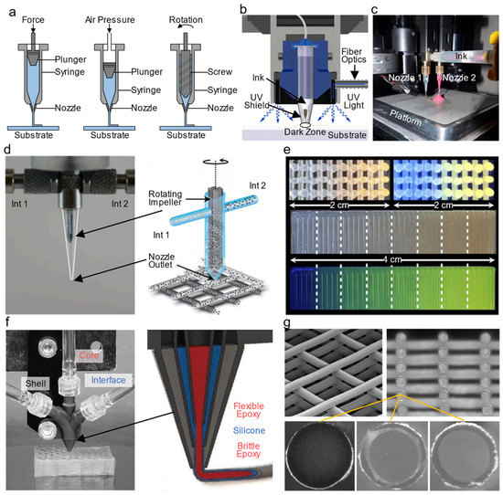
Figure 2b shows a modified UV-assisted DIW setup [
128].
Figure 2. (
a) Schematics of plunger-based extrusion, pneumatic-based extrusion, and screw-based extrusion of DIW. (
b) Cross sectional view of the UV-assisted DIW process [
128]. (
c) Multi-material 3D printing with a dual nozzle DIW system [
133]. (
d) Optical image and schematic illustration of the impeller-based active mixer for multi-material DIW, and (
e) cross sectional images of the printed 3D rectangular lattice structure showing continuous change in the fluorescent pigment concentration [
134]. (
f) Optical image and schematic illustration of the multicore-shell nozzle connected to the core, interface, and shell ink syringes for multi-material DIW, and (
g) cross sectional images of the printed rectangular lattice structure [
138].
Various material and process parameters, for instance, the rheological properties of the ink (e.g., viscosity and surface tension), the geometric features of the nozzle, extrusion pressure, standoff distance, printing speed, strip spacing, and curing technique, significantly dictate the quality (e.g., dimensional error, surface roughness, layer flatness, and interfacial strength) of the printed 3D parts [
129,
130]. Several essential criteria of qualified inks for DIW include the ability to flow easily through the nozzle when subjected to a shear force, sufficient yield strength after extrusion, and self-supportability. The feature resolution is positively correlated with the size of the nozzle. Although smaller nozzles provide higher feature resolution, they sacrifice build efficiency, and a greater extrusion pressure is required to enable smooth flow of the viscoelastic ink at the risk of nozzle damage. Notably, DIW with a nozzle diameter ranging from 0.5 µm to 5 µm has been used to create structures with feature sizes ranging from 100 nm to 10 µm [
131].
There are three different strategies enabling multi-material 3D printing with DIW (multi-material DIW) according to the nozzle design and ink extrusion mode. The first is that multiple inks stored separately in their individual syringes are extruded through multiple nozzles to construct multi-material structures layer-by-layer (
Figure 2c) [
132,
133]. This strategy is the most commonly used and involves switching between multiple nozzles for sequential printing, which requires accurate coordination of each nozzle and careful flow control of viscoelastic inks, especially when the printed inks have different rheological properties [
21]. The second uses a single nozzle with the capability of switching between inks or in situ mixing of multiple inks via a mixing impeller driven by rotary motor during the printing process while simultaneously controlling the printed geometry (
Figure 2d–e) [
134,
135,
136]. This strategy makes it possible to fabricate functionally graded patterns with tunable properties (e.g., strength, coefficient of thermal expansion, and permittivity). The third strategy uses a multicore-shell nozzle with several specific inputs connected to corresponding syringes, which enables the coextrusion of multiple inks to form a core-shell filament (
Figure 2f–g) [
137,
138].
Recently, multi-material DIW has been increasingly adopted to manufacture functionally graded structures (e.g., triboelectric nanogenerators [
139], sensors [
140], supercapacitors [
141,
142], photodetectors [
143], batteries [
132], circuit board [
144], and scaffolds [
145]) because of its unique ability to separately or simultaneously extrude different functional inks. For example, Sears et al. [
145] used a multi-material DIW printer to fabricate a scaffold with a poly(ε-caprolactone) (PCL) or poly(lactic acid) (PLA) shell and a propylene fumarate dimethacrylate (PFDMA) hierarchical architecture. The addition of the PCL or PLA shell resulted in a significant increase in the compressive modulus and yield strength. Natural bone tissue comprises hierarchical porous structures that support cell growth, provide space for nutrient transport, and withstand different types of ambient loads [
146]. Critical size or non-union bone defects can be treated by surgically implanting biocompatible bone graft substitutes [
147]. However, there are many problems in the long-term use of biocompatible bone graft substitutes, such as displacement, allergic reaction, and the need for secondary surgery [
148]. Another permanent solution is to facilitate bone tissue regeneration via a scaffold. Multi-material DIW has garnered considerable attention because of its potential in constructing the heterogeneous and anisotropic structure that can enable scaffolds to mimic the properties of natural bone tissue [
123,
149]. In addition, triply periodic minimal surface (TPMS) scaffolds allow for precise geometric modification; as a result, many physical characteristics (e.g., surface-to-volume ratio, pore size, elastic properties, and fluid behaviors) can be controlled [
150].
2.3. Fused Deposition Modeling (FDM)
FDM is one of the most extensively used 3D printing techniques for polymer structures (e.g., polylactic acid, butadiene styrene, polycarbonate, polyamide, polystyrene, and polyethylene [
151]) because of its inexpensive apparatus cost and easy implementation. FDM is also known as fused filament fabrication (FFF); in this process, the thermoplastic polymer filament is melted or softened in a liquefier head, and then the polymer is selectively extruded by the action of two counter rotating elements on the platform to build the 3D objects in a layer-on-layer manner. Over the past few years, thermoplastic polymer filaments reinforced by a variety of fillers, such as metals [
152,
153], ceramics [
154,
155,
156,
157], fibers [
158,
159], and bioactive glass [
160], have been developed. With enhanced properties (e.g., mechanical strength, thermal conductivity, permittivity, dielectric loss, and biocompatibility) of these composite filaments, FDM greatly expands its application scope into electronic, automotive, aerospace, biomedical, and sports industries.
The critical parameters of FDM are filament-specific (e.g., thermal, mechanical, and rheological properties and diameter), operation-specific (e.g., temperature, speed, and structure of 3D-printed object), and apparatus-specific (e.g., number of extrusion heads, nozzle diameter, and gear force) [
161,
162]. Multi-material 3D printing with FDM (multi-material FDM) can be easily implemented using multiple extrusion nozzles, and the method has drawn increasing interest. However, some inherent disadvantages still exist when multi-material FDM is used to construct complex structures, such as low resolution accompanied by poor surface finish, insufficient bonding between adjacent sections, and slow build velocity [
21]. Additionally, thermoplastic polymer filaments with high solid content are necessary for the fabrication of metal and ceramic parts because of the low shrinkage after sintering; However, the dramatic increase in stiffness and brittleness adversely affects the production and printing process [
163]. Therefore, significant efforts should be devoted to overcoming these challenges.
2.4. Vat Photopolymerization (VP)
In the vat photopolymerization (VP) process, a liquid-state photopolymer material housed in a vat is selectively cured and patterned by light-initiated polymerization [
10]. This class of technologies includes stereolithography (SLA), two-photon lithography (2PL) or two-photon polymerization (2PP), digital light processing (DLP), and continuous liquid interface production (CLIP).
As one of the oldest VP technologies established by Hull in 1984, SLA uses a UV laser beam scanning quickly along a controlled path to cure the irradiated photopolymer material within a vat from point to point. After one slice is printed, the build platform moves downward or lifts (depending on if the machine is a top-down or bottom-up structure) with a constant amount equaling exactly one-slice thickness in the z-direction for the next slice printing until the 3D part is finished [
164]. Another important laser scanning technology, 2PL, differs from conventional (single-photon) SLA by exploiting the two-photon absorption (2PA) process to induce polymerization of the photopolymer material within the focal region of an ultrafast (femtosecond or picosecond) pulsed laser. Therefore, 2PL can be used to fabricate 3D microstructures with feature resolutions beyond the diffraction limit and free from the staircase effect caused by fluctuations of photopolymer materials [
165]. However, 2PL shares the same common time-consuming issue as SLA and requires careful design of the highly transparent feedstock, especially when involving light-scattering additives such as ceramic particles [
166].
In contrast to the aforementioned laser scanning technologies, DLP employs a digital light projector rather than a laser as the light source; as a result, a UV image corresponding to each layer shape can be projected over the surface of the photopolymer material within a vat. DLP considerably improves building efficiency because any design can be printed layer-by-layer instead of individually addressing one voxel. Projection micro stereolithography (PµSL) is a development from DLP using a liquid crystal display, a digital micromirror device, or liquid crystals on the silicon device as a dynamic mask and featuring superior resolution (up to 0.6 µm) [
167]. CLIP is another development from DLP enabling continuous growth of a 3D part using an oxygen-permeable and UV-transparent window at the bottom of the photopolymer material vat [
168]. Oxygen can travel through the window and mix into the liquid photopolymer material, forming a persistent liquid interface (oxygen dead zone) capable of inhibiting free radical photopolymerization. As a result, the build platform no longer needs to move up and down for each layer [
169].
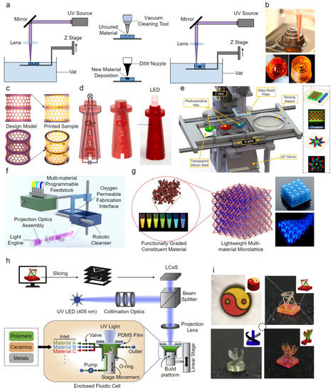
These VP-based 3D printing technologies have shown great potential in sensors, actuators, robots, microfluidic devices, and scaffolds because of their ability to construct 3D parts with high resolution, high accuracy, high throughput, and a good surface finish, which is not the case for MJ, DIW, and FDM [
170]. However, most studies simply focus on single-material fabrication, and multi-material 3D printing with VP-based technologies remains challenging and limited because of difficulties in exchanging liquid-state photopolymer materials within a vat. In general, three different strategies have been developed: (1) a hybrid process via the combination with DIW, AJP, or other special techniques, (2) vat switching, and (3) dynamic fluidic control. Among a few recently reported applications, the first strategy may be the most straightforward and widely adopted. Lopes et al. [
171] presented a hybrid multi-material 3D printing system that integrated SLA and DIW to fabricate monolithic structures with embedded circuits. SLA was used to build substrate structures, reserving the required receptacles into which electronic components were subsequently inserted, and channels and vertical vias were created, while DIW provided a precisely dispensing conductive material in the channels and vertical vias to realize interconnection (
Figure 3a). Similarly, Peng et al. [
172] presented a hybrid multi-material 3D printing system that integrated DLP and DIW to fabricate active soft robots, circuit-embedding architectures, and strain sensors (
Figure 3b–d). This strategy requires an effective cleaning tool (e.g., air jet, vacuum, brush, and ultrasonic) to remove the uncured photopolymer material from reserved receptacles, channels, and vertical vias, as any material contamination leads to dimensional inaccuracies. With the second strategy, the simplest approach is to manually or automatically exchange the photopolymer material within a vat [
173] or switch between multiple vats containing different photopolymer materials [
174,
175]; however, the printing process has to be interrupted, significantly increasing its time consumption. To overcome this issue, researchers have proposed multi-material stereolithography without vats that can deliver multiple photopolymer materials on a moving glass plate or silicone sled using aerosol jet systems [
176] or pump-based syringes [
177,
178,
179] (
Figure 3e). In this distinctive process, a bottom-up projection method is mostly adopted, which greatly reduces the amount of residue to be cleaned because the printed part is immersed in the liquid-state photopolymer material at a limited depth [
180]. Notably, in combination with an in situ microfuidic system (
Figure 3f), Chen et al. [
181] achieved 3D microlattices with dissimilar constituent materials (
Figure 3g), which is attractive for manufacturing various structures with tailorable properties such as a negative Poisson’s ratio. Miri et al. [
182] demonstrated an in situ microfuidic system with several on/off pneumatic valves for fast switching between different photopolymer materials and accomplished the multi-material stereolithography of heterogeneous hydrogel constructs. With the third strategy, recently, Han et al. [
183] developed a multi-material PµSL system using dynamic fluidic control to realize rapid filling and exchange of multiple photopolymer materials within an integrated pressure-tight fluidic cell (
Figure 3h) that is capable of fabricating highly complex heterogeneous 3D microstructures (
Figure 3i).
Figure 3. Multi-material 3D printing with VP-based technologies. (
a) Schematic illustration of the multi-material 3D printing system integrating SLA and DIW. (
b) Photographs of the printed electronic structure with an embedded 3D helix, (
c) photographs of the printed cylindrical lattice with three rings embedded, and (
d) photographs of the printed light tower [
172]. (
e) Schematic illustration of the multi-material stereolithography without vats [
179]. (
f) Schematic illustration of the multi-material stereolithography using an in situ microfuidic system, and (
g) photographs of the printed 3D microlattice with dissimilar constituent materials [
181]. (
h) Schematic illustration of the multi-material PµSL system using dynamic fluidic control to rapidly fill and exchange multiple photopolymer materials, and (
i) photographs of the printed micro 3D structures [
183].
3. Applications of Multi-Material 3D Printing in Functional Ceramic Devices
In most cases, functional ceramic devices with multiple material constituents have tiny structural features such as strip lines, microstrip lines, and vias. These structural features present a challenge for multi-material 3D printing processes because micro-defects will degrade the electrical and mechanical properties. In addition, the materials (ceramics, polymers, and metals) and their compatibility with 3D printing techniques must be further investigated. Table 2 lists several composition examples of multi-material 3D printing in functional ceramic devices.
Table 2. Several composition examples of multi-material 3D printing in functional ceramic devices.