Your browser does not fully support modern features. Please upgrade for a smoother experience.
Submitted Successfully!
 +1 credit
Thank you for your contribution! You can also upload a video entry or images related to this topic.
For video creation, please contact our Academic Video Service.
| Version | Summary | Created by | Modification | Content Size | Created at | Operation |
|---|---|---|---|---|---|---|
| 1 | William Chiappim Junior | -- | 7343 | 2022-10-18 15:10:24 | | | |
| 2 | Beatrix Zheng | -2227 word(s) | 5116 | 2022-10-19 03:33:10 | | |
Video Upload Options
We provide professional Academic Video Service to translate complex research into visually appealing presentations. Would you like to try it?
Cite
If you have any further questions, please contact Encyclopedia Editorial Office.
Chiappim, W.; Neto, B.B.; Shiotani, M.; Karnopp, J.; Gonçalves, L.; Chaves, J.P.; Sobrinho, A.D.S.; Leitão, J.P.; Fraga, M.; Pessoa, R.; et al. Plasma-Assisted Atomic Layer Deposition in Nanofabrication. Encyclopedia. Available online: https://encyclopedia.pub/entry/29959 (accessed on 14 June 2026).
Chiappim W, Neto BB, Shiotani M, Karnopp J, Gonçalves L, Chaves JP, et al. Plasma-Assisted Atomic Layer Deposition in Nanofabrication. Encyclopedia. Available at: https://encyclopedia.pub/entry/29959. Accessed June 14, 2026.
Chiappim, William, Benedito Botan Neto, Michaela Shiotani, Júlia Karnopp, Luan Gonçalves, João Pedro Chaves, Argemiro Da Silva Sobrinho, Joaquim Pratas Leitão, Mariana Fraga, Rodrigo Pessoa, et al. "Plasma-Assisted Atomic Layer Deposition in Nanofabrication" Encyclopedia, https://encyclopedia.pub/entry/29959 (accessed June 14, 2026).
Chiappim, W., Neto, B.B., Shiotani, M., Karnopp, J., Gonçalves, L., Chaves, J.P., Sobrinho, A.D.S., Leitão, J.P., Fraga, M., Pessoa, R., & Junior, W. (2022, October 18). Plasma-Assisted Atomic Layer Deposition in Nanofabrication. In Encyclopedia. https://encyclopedia.pub/entry/29959
Chiappim, William, et al. "Plasma-Assisted Atomic Layer Deposition in Nanofabrication." Encyclopedia. Web. 18 October, 2022.
Copy Citation
The growing need for increasingly miniaturized devices has placed high importance and demands on nanofabrication technologies with high-quality, low temperatures, and low-cost techniques. The development and advances in atomic layer deposition (ALD) processes boosted interest in their use in advanced electronic and nano/microelectromechanical systems (NEMS/MEMS) device manufacturing. In this context, non-thermal plasma (NTP) technology has been highlighted because it allowed the ALD technique to expand its process window and the fabrication of several nanomaterials at reduced temperatures, allowing thermosensitive substrates to be covered with good formability and uniformity.
plasma-enhanced atomic layer deposition
plasma-assisted atomic layer deposition
plasma-assisted atomic layer etching
1. Deposition: Plasma-Assisted Atomic Layer Deposition
In this section, the researchers will briefly review the main applications of thin films grown by plasma atomic layer deposition (ALD). The focus of this section is to show the versatility of the plasma ALD technique in the deposition of different materials using different reactors, precursors, and present old and new applications.
1.1. Oxides
ALD is one of the most used techniques in photovoltaic (PV) technology, mainly for buffer layer growth (BFL) and passivation layers (PSL). These layers generally increase the rate of recombination by reducing interface defects, which increases power conversion efficiency (PCE). It is important to highlight that PV technology encompasses all existing technologies, such as silicon wafer-based PV [1], chalcogenide thin-film-based PV [2], III-V based PV [3], perovskite-based PV [4], dye-sensitized based PV [5], organic-based PV [6], and quantum dot solar cells [7]. However, new applications that go beyond BFL and PCE are being studied.
In 2016, Wang et al. [8] showed that tin oxide (SnO2) deposited at low temperatures by PA-ALD has an excellent electron selective effect in highly efficient organic-inorganic metal halide perovskite solar cells with a planar cell structure. Figure 1 shows the PCE as a function of the ALD cycle and temperature process, and as can be seen, the thickness that optimizes the PCE is 17 nm for SnO2.
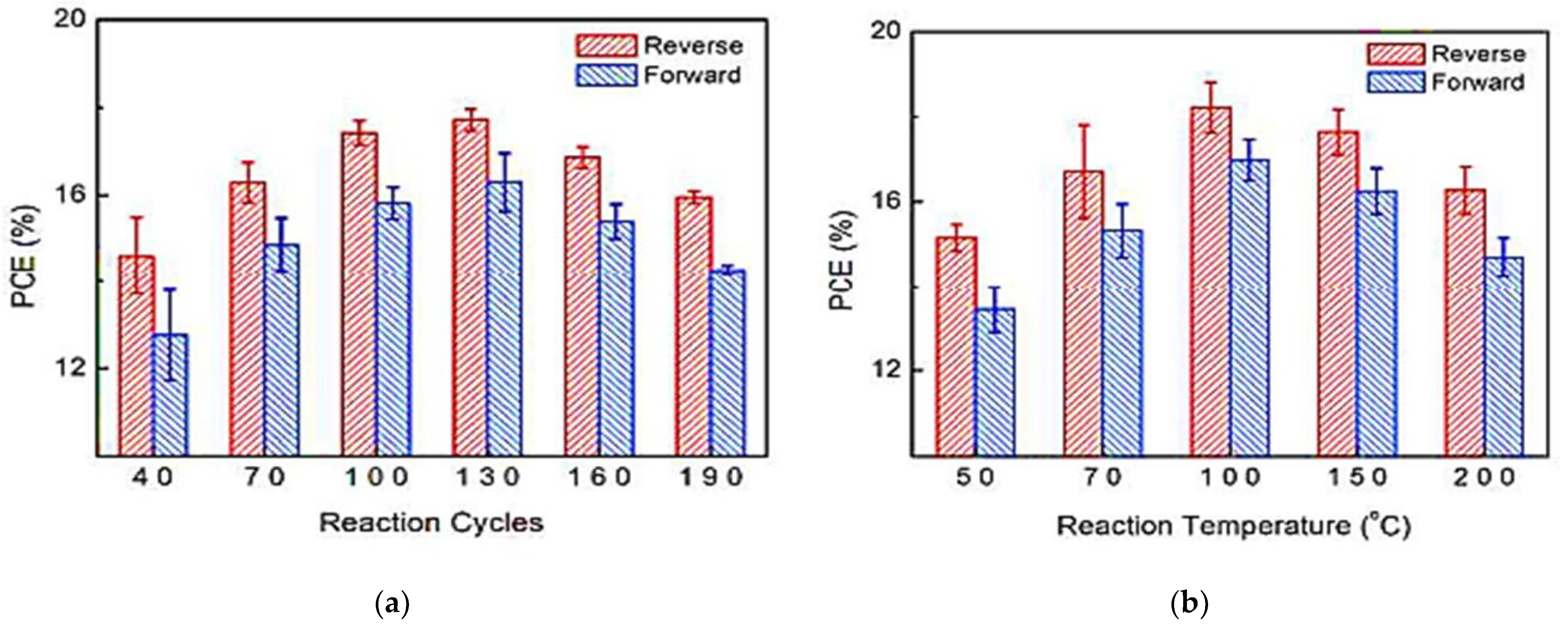
Figure 1. Power conversion efficiency (PCE) as a function of (a) reaction cycles; (b) process temperature. Reprinted with permission from Ref. [8]. Copyright 2016, Royal Society of Chemistry.
Tetrakis(dimethylamino)-tin(IV) was used as the Sn reactant, heating the precursor line to 75 °C. Pure O2 was used as the co-reactant, and ultra-pure argon (Ar) was used as the carrier gas with a flow rate of 15 sccm. The resulting growth per cycle (GPC) was about 0.17 nm/cycle. The importance of PA-ALD is due to the temperature reduction of the complex planar cell construction process, which reduces the associated costs. The electron selective layer (ESL) of SnO2 was deposited at 70 °C (chamber and substrate temperature), and a PCE of 19.03% for glass substrate and 16.80% for flexible polymer substrate was achieved. At this temperature, the SnO2 films that had grown were of excellent quality. This high quality at low deposition temperature enables the large-scale manufacture of efficient perovskite solar cells. In 2018, Reichel et al. [9] studied the PA-ALD of aluminum oxide (Al2O3) applied as surface passivation and electrical insulation on silicon solar cells. They carried out the experiments in a PA-ALD tool with a remote ICP at 140 W. Trimethylaluminum (TMA), and O2 plasma was used as a reactant and co-reactant, respectively. Argon (Ar) purge gas flow 30 sccm was applied. The deposition temperature varied from 100 to 350 °C, with a GPC decrease of 0.16 to 0.1 nm/cycles for the highest temperature. ALD cycles were chosen to generate thin films with thicknesses of about 10 nm to almost 250 nm. They studied the pinhole density and the stress of the thin films as deposited and after annealing from 250 to 450 °C. Despite Al2O3 thin films being much explored as PSL, the authors’ approach is interesting because the annealing step at 450 °C to films deposited at 250 °C with thickness at least 80 nm presented a low defect density and low stress avoiding a leakage current and generating a high breakdown voltage. These parameters make the Al2O3 thin films grown by PA-ALD a promising candidate for silicon solar cells that rely on passivating and insulating thin films. In 2020, Wang et al. [10] showed interesting applications of PA-ALD in perovskite solar cells. In contrast to the increase in PCE, perovskite technology suffers from low stability and high toxicity [11]. These questions are the main challenges in the commercialization of perovskite solar cells, despite the constant improvement in the long-term stability of perovskite solar cells, including changes in interface physics, compositional changes, and passivation in the grain boundary. Perovskite quickly degrades in contact with moisture and despite being a promising technology, it barely can support practical applications. In this context, the authors used a new efficient device encapsulation technique to prevent moisture degradation and prolong operational life in a natural environment. The method uses PA-ALD to create an anti-water encapsulation deposited on the perovskite solar cells. Ethyl glycol was first deposited as BFL by molecular layer deposition (MLD), followed by Al2O3 PA-ALD deposited at 50 °C to prevent possible degradation of metal halide perovskite solar cells. TMA and O2 plasma were the reactants of Al2O3, with Ar as the purge gas. The plasma power was fixed at 100 W. The ALD pulses were 0.04–80–10–120 s, respectively, TMA-Purge-O2 plasma-Purge. The authors showed that the encapsulation structure exhibited a water vapor transmittance rate (WVTR) of 1.3 × 10⁻⁵ g.m2⋅day−1, the lowest value among thin-film encapsulation layers reported in the literature for solar cells. They also demonstrated that the perovskite solar cells withstood 80% relative humidity (RH) at a temperature of 30 °C for over 2000 h with a 96% preservation of their initial PCE (see Figure 2).
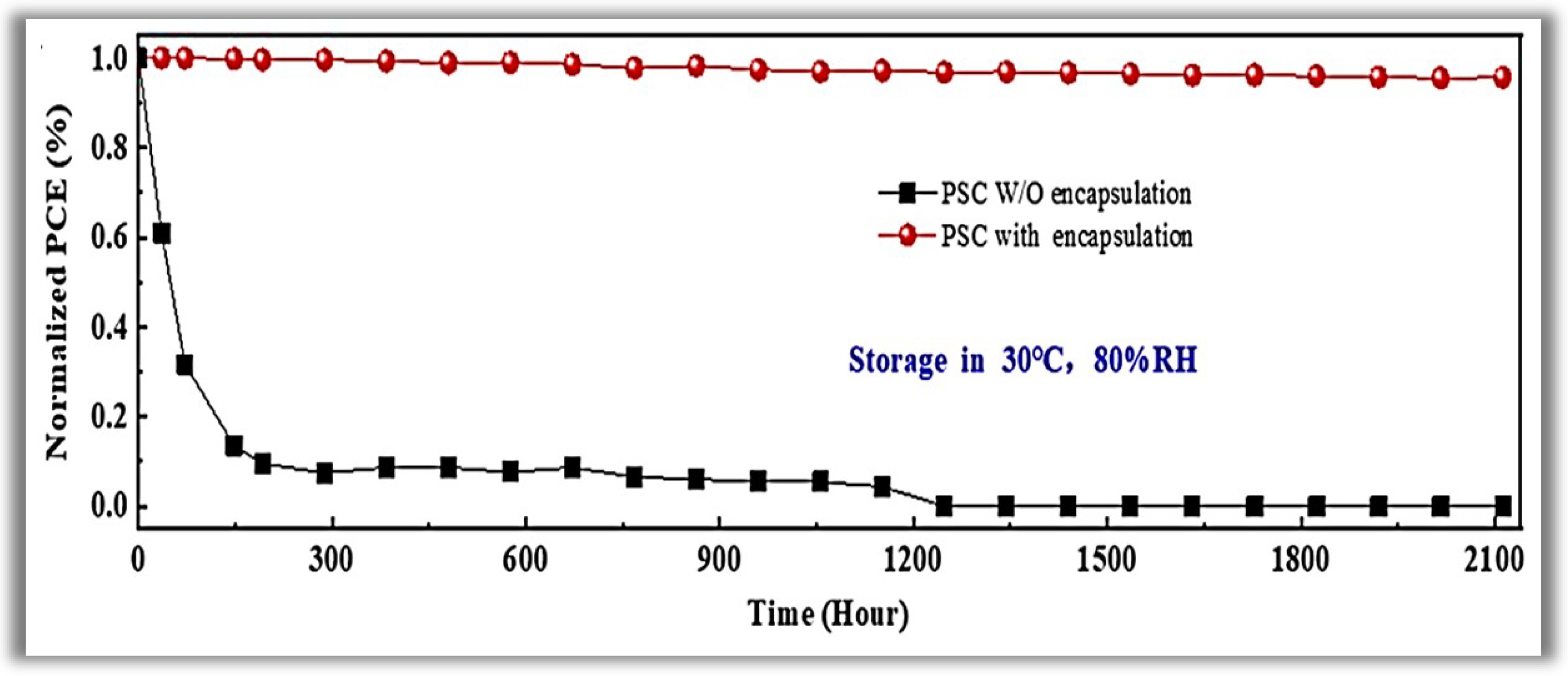
Figure 2. Time evolution of power conversion efficiency for the perovskite solar cells with and without encapsulation under high humidity. Reprinted with permission from Ref. [10]. Copyright 2020, Elsevier.
Organic light-emitting diodes (OLEDs) are already a reality in flexible displays and displays marketed worldwide. Industrial and academic interest in research with OLEDs is growing due to their attractive requirements, which are [12]:
-
Wide viewing angle.
-
Low latency.
-
Low power consumption.
-
Ultra-thin lightness and thickness.
-
Mechanically flexible.
However, vulnerabilities caused by contact with moisture and oxygen are still significant barriers. OLEDs are low-work function metal-based technologies that work with active layers of small molecules that are easily oxidized, crystallized, and delaminated after rapid exposure to oxygen and water. This fragility causes edge shrinkage and can also introduce dark spots [13]. As observed in the perovskite solar cells, the most viable solution is the efficient nanoencapsulation of the OLEDs to prevent the penetration of water or oxygen, thus avoiding the degradation of the organic molecules. In this sense, PA-ALD allows for the controlled self-limited growth of high-density, with ultra-thin films conformal that grow at low temperatures by monolayer-by-monolayer with WVRT of about 1 × 10⁻⁶ g.m2⋅day−1, which is the necessary value for a perfect operation of OLEDs.
In 2016, Hoffmann et al. [14] were the first to publish a study of thin-film gas permeation barriers based on Al2O3 cultured by atmospheric pressure plasma-enhanced atomic layer deposition (APPALD). The work was not applied directly to OLEDs but opened the way for new applications. The authors grew Al2O3 thin films using TMA, and Ar/O2 plasma at 80 °C. The substrates used for the analysis were polyethylene terephthalate coated with tin oxide and indium, another substrate used was Si. It is worth mentioning that these films were grown at atmospheric pressure and showed a WVRT of the order of 5 × 10⁻⁵ g.m2⋅day−1. In the same year, Kim et al. [15] examined the effects of the oxide ratio on the WVTR of Al2O3/TiO2 nanolaminate films (50 nm) prepared by PA-ALD. They used TMA as a precursor of Al2O3 and tetrakis-(dimethylamino)-titanium (TDMAT) as the precursor of TiO2. O2 plasma was used as an oxygen source for both precursors at 100 W. The authors demonstrated that the Al2O3/TiO2 nanolaminate film exhibited optimal properties for a 1:1 atomic ratio of Al2O3/TiO2 with the lowest value of WVTR of 9.16 × 10⁻⁵ g.m2⋅day−1 at 60 °C and 90% RH (shelf-life can be observed in Figure 3).
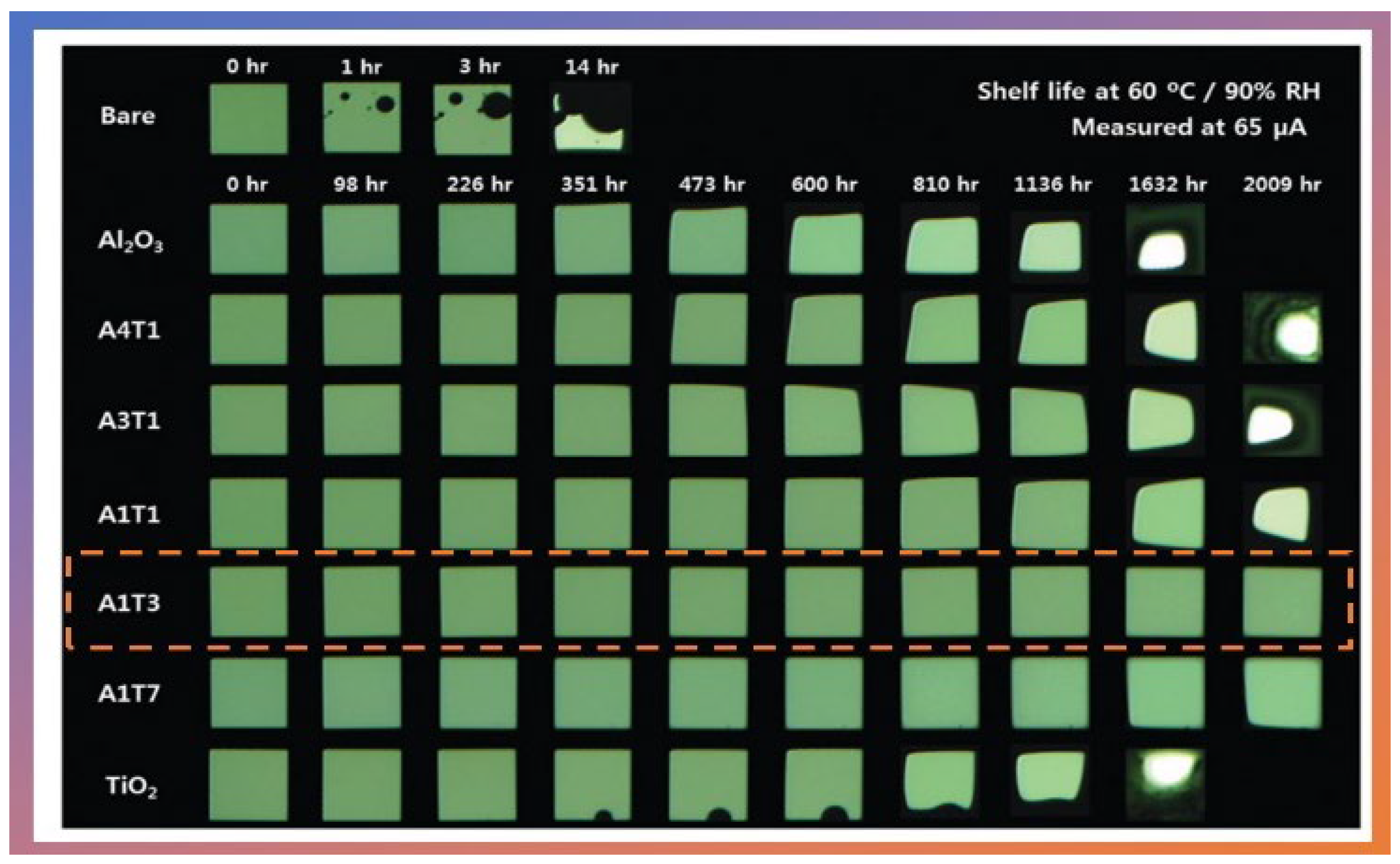
Figure 3. Shelf lives of the OLED devices passivated with and without Al2O3/TiO2 nanolaminates grown via PA-ALD. The A1T3 film highlighted represents the 1:1 atomic ratio of Al2O3/TiO2 with the lowest WVTR value at 60 °C and 90% of RH. Reprinted with permission from Ref. [15]. Copyright 2016, Royal Society of Chemistry.
OLED devices showed a most extended shelf-life, over 2000 h, without forming dark spots or edge shrinkage. In 2020, Jin et al. [16] studied the encapsulation of CsPbBr3 (perovskite) nanocrystals (NCs) using thin films of SiO2 grown by PA-ALD and showed that the optical performance of the device was minimally affected. The authors showed that the ALD layer effectively prevented the deformation and sintering of CsPbBr3 NCs, improving water, light, and heat stability. They proved that white LEDs encapsulated extended the color gamut to 126% NTSC, suggesting potential application as wide color gamut LED backlights. Therefore, it is clear that the encapsulating used in OLEDs and LEDs by PA-ALD shows promising results and has great industrial appeal.
The most traditional application of oxides grown by PA-ALD is in micro/nanoelectronics. The most conventional devices that take advantage of PA-ALD are transistors, capacitors, and non-volatile memories. Below is a summary of the main applications of PA-ALD:
- (1)
-
Yeom et al. [17] grew indium oxide (InOx) using Et2InN(SiMe3)2 and O2 plasma as reactants. The deposition temperature varied between 100 and 250 °C with a GPC of 0.145 nm/cycle. The authors showed that thin-film transistors (TFTs) built with nano-crystalline InOx had a higher carrier density as the temperature ramp increased from 150 to 250 °C. This effect is due to oxygen deficiency at higher deposition temperatures. The TFTs showed high linear mobility of 39.2 cm2 V−1 s−1 for nano-crystalline InOx grown at 250 °C. Therefore, this result indicates that InOx TFTs are a strong candidate for next-generation high-performance TFTs.
- (2)
-
Egorov et al. [18] used PA-ALD for TaOx deposition with a controllable concentration of oxygen vacancies (VO). Ta(OC2H5)5 was used as a reactant of Ta, and Ar/H2 plasma as a co-reactant. The VO control made through the fractional mixture of Ar and H2 in the plasma generation was responsible for controlling the leakage current of the resistive switching memory devices in the range of five orders of magnitude compared to the Ta2O5 film grown via thermal ALD. Ultimately they used the Ta2O5/TaOx stack with reliable resistance switching up to approximately 106 switching cycles, in contrast to the single-layer Ta2O5 memory, which demonstrated an order of a few hundred switching cycles.
- (3)
-
Jha et al. [19] grew HfO2 thin films by PA-ALD for non-volatile memory applications. For this, they investigated the electrical and ferroelectric properties of metal-insulator-semiconductor (MIS) and metal-insulator-metal (MIM) capacitors with different thicknesses between 5 and 20 nm deposited on Si and TiN/Si. The best results were achieved for 10 nm films. A memory window of 4 V was found for the MIS structure and the MIM structure, with a maximum remaining polarization of 4 μC/cm2. The non-volatile memories based on HfO2 thin films showed a data retention structure of more than ten years with a fatigue resistance of 1012 read/write cycles.
- (4)
-
Henning et al. [20] used an aluminum oxide monolayer (~0.3 nm) deposited by PA-ALD for gallium nitride encapsulation in the c-plane (GaN), which is enabled by the partial conversion of surface oxide GaN to AlOx using sequential exposure to trimethylaluminum (TMA) and H2 plasma. This thin AlOx monolayer decreases the work function that increases the reactivity with phosphonic acids under standard conditions, leading to self-assembled monolayers with densities close to the theoretical limit. This high reactivity of TMA with surface oxides opens the opportunity to extend this ultra-fine (<1 nm) aluminum oxide deposition approach to other III-V-based dielectrics and semiconductors, with relevance for applications in (photo) electrocatalysis, optoelectronics, and chemical sensing.
- (5)
-
Xiao et al. [21] studied the effect of HfO2 and ZrO2 on n-channel p-channel metal oxide semiconductor field-effect transistors (nFETs and pFETs), CMOS inverters, and CMOS ring oscillators were fabricated to test the quality of HfO2 thin films, and ZrO2 applied as a gate oxide. They used tetrakis(dimethylamino), hafnium (Hf[N(CH3)2]4), and tetrakis (dimethylamino) zirconium (IV) (Zr [N(CH3)2]4) as precursors, respectively, of Hf and Zr. The manufactured nFTTs and pFETs have good electrical properties of n or p-type field-effect transistors, while CMOS inverters based on HfO2 and ZrO2 have good electrical transfer characteristics. Both manufactured ring oscillators demonstrated satisfactory oscillation waveforms, and the ZrO2 gate oxide caused the oscillator to oscillate faster than the HfO2 gate oxide.
1.2. Nitrides
Like oxides, nitrides are also extensively studied and applied in a range of fields of modern technology, ranging from dielectric barriers to corrosion-resistant films. In this section, the researchers will cover some applications of nitrides grown by PA-ALD. Initially, the researchers will address applications of Al, Ti, and Si-based nitrides.
For example, the application performed by Otto et al. [22] in 2016, where PA-ALD was used to deposit TiN films. They showed the possibility of using it as a promising synthetic plasmonic metal. TiN thin films are an alternative to the plasmonic community with an immediate need to supply traditional plasmonic materials, such as Ag and Au, which have low mechanical, thermal, and chemical stability. Synthetic metal and plasmonic alloys have better stability, but they require growth temperatures > 400 °C, making the use of technological substrates that are generally sensitive to high temperatures unfeasible. In this sense, the work presented by Otto and co-workers using PA-ALD at low temperatures is very important for the area in question. This work used tetrakis(dimethylamino)titanium (TDMAT) as Ti precursor, and N2/H2 plasma was used as N precursor. Through optical measurements and theoretical modeling, it was demonstrated that the plasmonic network performance had a period of 900 nm. In 2018, Krylov et al. [23] deposited TiN films by PA-ALD and obtained films with low resistivity. According to studies, electron scattering on grain boundaries is the dominant mechanism. This mechanism is a determinant for the low resistivity of TiN films, and it is necessary to obtain large grains in the columnar form to reduce resistivity further. These two examples are essential to see how the same technology and films can be applied in different fields. Kim et al. [24] used PA-ALD to grow SiNx thin films used as 10 nm thick dielectric barriers to prevent the diffusion of Cu into SiO2/barrier/Cu/TaN structures on Si substrates. A direct plasma ALD process was used with trimethylsilane (TMS) as the Si precursor, NH3 plasma, and He as the purge gas. Although PA-ALD SiNx film has a low dielectric constant (<5), the layer’s ability to prevent Cu diffusion was equivalent to that of plasma-enhanced chemical vapor deposition (PECVD) SiCN. This result shows the feasibility of immediately replacing traditional PECVD-grown SiCN films with PA-ALD SiNx in thin dielectric barrier devices for future advanced technologies. Seppänen et al. [25] used a new approach to grow aluminum nitride (AlN). First, the film is developed by PA-ALD with a plasma power of 100 and 200 W. After film growth, in situ atomic layer annealing (ALA) is used. This possibility of growing crystalline films using ALA to form better quality nucleation layers for further growth of nitride compounds is an essential approach for applications in the semiconductor industry.
Han et al. [26] used a novel complex precursor bis((2 (dimethylamino)ethyl)(methyl)amino)methyl(tertbutylimido)tantalum for growth of tantalum nitride (TaN) films. PA-ALD used NH3 plasma, and the growth temperature varied between 150 and 250 °C with 0.062 nm GPC. They showed that ultrathin TaN films (2 nm) have a film density of 9.1–10.3 g/cm3 at 200–250 °C. Despite only 2 nm, the Cu barrier performance of the TaN film showed excellent properties when evaluated by annealing between 400 and 800 °C. The properties of TaN are comparable to SiNx (10 nm) presented by Kim et al. [24].
Wang et al. [27] developed zirconium nitride (ZrN) + zirconium oxide (ZrO2) alloys by PA-ALD to be applied as thin films with high corrosion resistance. The new zirconium oxynitride (Zr2N2O) coating was deposited on 304 stainless steel (SS) by incorporating a controlled amount of oxygen into ZrN using PA-ALD. The main idea of this work is to solve a double problem involving the susceptibility to corrosion of metallic bipolar plates that limits their application in polymer electrolyte membrane fuel cells (PEMFCs). The candidate material to solve this problem must be conductive and have high corrosion resistance. In this context, zirconium nitride (ZrN) exhibits increased corrosion resistance but lacks conductivity. In contrast, ZrO2 is a good conductor but has low corrosion resistance. Therefore, the solution adopted by the authors to build Zr2N2O thin films proved to be very promising, as the corrosion current density of the specimen coated with Zr2N2O has an order of magnitude smaller than that of the substrate coated with ZrN. And in long-term testing, the interfacial contact resistance (ICR) of the Zr2N2O coated specimen is much lower than that of the ZrN coated sample due to improved oxidation resistance. As shown in Figure 4, the potentiodynamic polarization curves show that the adopted strategy produces thin films with an ultra-high corrosion resistance with considerable conductivity.
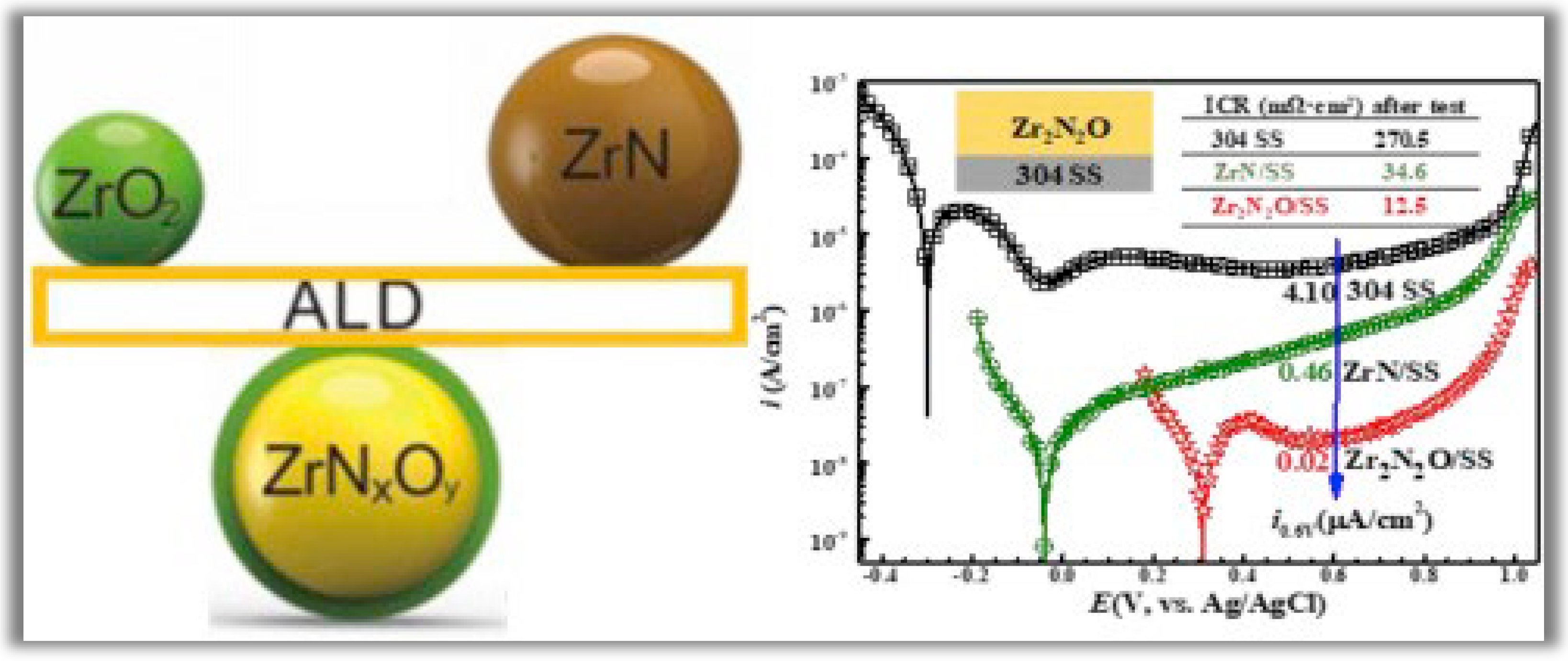
Figure 4. Potentiodynamic polarization curves of 304 stainless steel (SS), ZrN/304 SS, and Zr2N2O/304 SS. Reprinted with permission from Ref. [27]. Copyright 2018, Elsevier.
Sowa et al. [28] and Tian et al. [29] grew thin films of niobium nitride (NbN) that have excellent physical, chemical, and electrical properties. NbN PA-ALD were deposited with (tert-butylimido)-tris(diethylamino)niobium as the Nb reactant and plasma H2/N2 and H2/NH3 as the N source. Sowa et al. used temperatures between 100 and 300 °C and powers ranging between 150 and 300 W. At high deposition temperatures, the 350 nm thick films had more significant cubic NbN crystals and had higher density with resistivity at room temperature of the order of 173 μΩ.cm and with superconductivity analysis of 13.7 K. Tian et al. used temperatures between 200 and 400 °C and plasma power fixed at 2800 W. The annealing of the films was used (50 µm thick) to improve the crystallinity and was carried out in an Ar environment with temperatures ranging between 800 and 1200 °C and exposure times varying from 10 to 60 min. The efficiency of superconducting radiofrequency cavities composed of Nb improved after thermal annealing up to 13.8 K, a value compatible with the desired application. An increase in density was also observed, as well as an increase in grain size.
1.3. Sulfides, Phosphates and Others
Sulfide-based thin films started to stand out, mainly due to the technological appeal of materials such as tungsten disulfide (WS2) and molybdenum disulfide (MoS2), which can revolutionize nanoelectronics [30].
Transition metal-based 2D dichalcogenide, more precisely, WS2, is a potential low-dissipation semiconductor material for nanoelectronic devices. However, applications of these materials in nanoelectronics require the materials to grow in crystalline form with the number of monolayers controlled and at low temperatures. In this sense, PA-ALD meets these requirements. Groven et al. [31] grew strong textured nanocrystalline WS2 at 300 °C. The PA-ALD reaction cycle consisted of a WF6 reaction, an H2 plasma reaction, and an H2S reaction. They reported that the H2 plasma was essential as it reduced surface species −W6 + Fx. In 2019, Balasubramanyam et al. [32], intending to apply WS2 as electrocatalysts for the sustainable production of H2 through the electrochemical reaction of hydrogen evolution (HER), improved the quality of the deposited films by mixing H2+H2S as plasma-generating gas in PA-ALD. This approach adopted by the authors helped in satisfactory control of the edge location density and increased the HER performance of the edge-enriched WS2 electrocatalyst.
Recently, Sharma et al. [33] and Vandalon et al. [34] synthesized MoS2 and Al-doped MoS2 films at low temperatures, respectively. These extrinsically doped 2D and 2D semiconductors are essential for the fabrication of high-performance nanoelectronics. Sharma et al. used PA-ALD to grow thick MoS2 films from monolayer to multilayer at low temperatures. In contrast, Vandalon et al. synthesized Al-doped MoS2 thin films, resulting in a particularly sought-after p-type 2D material. They showed precise control over carrier concentration in the range of 1017 to 1021 cm−3. In the article by Vandalon and co-workers, it is evident that fine control over doping concentration, combined with compliance and uniformity and the sub-nm thickness control inherent in PA-ALD, ensures compatibility with the large-scale manufacture of this material technological.
Cadmium sulfide (CdS) based buffer layers are well established in thin-film photovoltaic technologies, particularly in Cu(In,Ga)Se2 (CIGS), CuZnSn(S,Se)4 (CZTSSe), and CuZnSnS4 (CZTS) type solar cells. However, the new environmental regulations suggested by the UN and proposed by the European Union (EU) [35] indicate the development of solar cells without toxic materials, such as Cd. CdS have other disadvantages that accelerate the change process, ranging from losing absorbed light due to the high recombination of minority carriers to decreased PCE. In this sense, new BF layers need to be presented and studied. Bugot et al. [36] proposed the growth of ultrathin films of InxSy and In2(S,O)3 grown by PA-ALD, which can be implemented as ultrathin interfacial buffer layers in CIGS solar cells. Films were produced using indium acetylacetonate(In(acac)3), hydrogen sulfide, and an Ar/O2 plasma as indium, sulfur, and oxygen precursors. The authors showed a study that led to a readjustment of the deposition conditions of In2(O,S)3 thin films allowing the promising implementation as buffer layers in CIGS solar cells with high PCE.
The versatility of PA-ALD allows the constant creation of new alloys or deposition of metals on 3D structures. This behavior allows for continuous evolution in nanoelectronics and spintronics. Wang et al. [37] grew Ti0.28Sb2Te3 (TST) based films by PA-ALD that can be used as a storage class memory phase change (SCM) material. They showed that due to the fast crystallization and the low melting temperature of the TST, the response speed decreased to 6 ns, while the reset voltage could be reduced by 20% compared to the Ge2Sb2Te5 (GST) based device with the same cell structure. These results indicate that TST thin films synthesized with PA-ALD are a fast and scalable phase change material that can be applied to SCM.
Giordano et al. [38] used PA-ALD to prepare thin films of formed nickel and nanotubes using nickelocene as a reactant, water as a co-reactant agent, and a plasma-enhanced reduction step cycled with H2, which is crucial for single material deposition. They fabricated several micrometer-long nickel nanotubes with diameters ranging from 120 to 330 nm (Shown in Figure 5). Their results show that the spin-wave damping was low, allowing detection of several stationary spin-wave modes, which fulfilled the condition of constructive interference in the azimuthal direction of a nanotube. Therefore, Ni planar films and nanotubes exhibited physical properties promising for functional spintronic elements and magnetic applications in 3D device architectures.
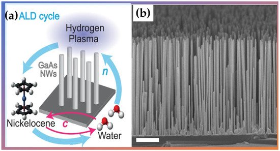
Figure 5. (a) Schematic ALD cycle used to synthesize nickel (Ni) nanotubes and (b) the scanning electron microscopy (SEM) micrographs of an ensemble of vertical nanowires with PA-ALD-grown Ni shells. Adapted from Ref. [38] with permission by Creative Commons 4.0.
2. Modification: Surface Modification on Polymers
NTP technology is widely used in the surface modification of polymers to bring the desired functionality to the polymer surface. However, the inhomogeneity and hydrophobicity of some polymers are incompatible with other substances necessary for the further functionalization of the polymer. DBD and gliding arc (GA)-based plasma generator reactors are commonly used in an attempt to overcome these problems that reduce functionalization [39][40]. The modification generated by these types of plasma can lead to a chemically unstable and non-uniform surface, which results in a low to moderate performance in the final application [41]. In this context, PA-ALD at low temperatures has low reaction rates, which result in low deposition rates. These unique features added to the ability to deposit ultra-thin films, making PA-ALD an essential tool in the surface modification of polymers, being a helpful way to bring the desired functionality to the polymer surface. However, some technical problems need to be overcome. Unlike hard inorganic surfaces that are commonly used as substrates in PA-ALD and have many reactive sites that promote film growth, reactive sites may or may not be present in the case of polymers. There is small molecule permeability in many polymers, allowing for the diffusion of PA-ALD precursors into and out of the polymer substrate subsurface [41]. Thus, the researchers can classify two polymer types: those that imitate a solid surface and have several reactive sites for film growth and the others that result in different final products. It is noteworthy that although reactive sites facilitate chemisorption between gas molecules and reactive functional groups on the surface, this does not always lead to smooth conformal growth as expected for PA-ALD on a solid and inorganic substrate [42]. In most polymers, the precursor diffuses to the sub-surface, causing rough surface texture, polymer swelling, and particle growth below the surface [43]. Therefore, this section will discuss recent studies of polymer functionalization by PA-ALD, showing that the surface reactions will depend on the nature of the polymer, the chemistry of the precursor and co-reactant, and the parameters of the plasma used in the process.
Semi-crystalline polymeric substrates such as polyethylene terephthalate (PET) and polyethylene naphthalate (PEN), and amorphous substrates such as polyethersulfone (PES), due to their transparency and flexibility, are gaining attention as promising materials applied to flexible devices. PET coated with transparent conductive oxides is applicable in OLED devices [44]. PEN coated with carbon nanotubes is used as flexible solar cells, OLEDs, and touch panels [45]. PES have high thermal resistance for operation at high temperatures, so they have great appeal in flexible optoelectronics [46]. However, these semi-crystalline or amorphous polymers have many technical problems to be solved. In particular, moisture and oxygen permeation damage substrates, reducing the life of OLEDs, flexible solar cells, and touch panels. The cited problem is avoided or mitigated by the use of permeation barriers which are usually oxides. In 2017, Kim et al. [43] and Fang et al. [47] used low-temperature PA-ALD to study the barrier properties of fine oxides. Kim and co-authors showed that the WVTR of the Al2O3 layer deposited on the plasma-treated PEN substrate was about 7.2 × 10⁻⁴ g.m2⋅day−1, which was significantly lower than that of the untreated substrate. Prior to PA-ALD, they pre-treated the polymer substrates with argon and oxygen plasmas to increase the number of reactive sites and facilitate the formation of polar groups that are crucial in the PA-ALD process. Fang et al. significantly reduced the WVTR to less than 10−3 g.m2⋅day−1 without a long-term cooling process, for PET substrates. A similar study was carried out by Lee et al. [48], but the material chosen was SiO2 grown by PA-ALD. They reduced the WVTR to 7.73 × 10⁻⁵ g.m2⋅day−1, which was 10 times lower than a control sample. Therefore, the growth of oxides by PA-ALD significantly enhances the protective barrier on flexible devices.
Kovacs et al. [49] presented in situ gas permeation measurements to study the cracking of oxide films grown on low-density polyethylene. They investigated the application of nanoscopic defects in Al2O3 thin films deposited by PA-ALD in polymeric electrolyte fuel cells. They showed that this mechanical limitation, which can impair their encapsulation utility, is critical in the case of polymeric electrolytic fuel cells containing a proton exchange membrane, where water retention in the membrane is crucial for the efficient transport of hydrated ions. Kovács and co-workers demonstrated that these nano-cracks could act as nano valves at low humidity levels and maintain the proper humidity level for the membrane.
In 2021, Sun et al. [50] proposed a new strategy for designing and manufacturing new integrated portable electronics. In contrast to previously reported studies that focus on encapsulation of devices. Sun and co-workers present a promising way to manufacture integrated, flexible, multifunctional sensors. Due to toughness and environmental stability, they used poly(vinylidene fluoride) (PVDF) as a polymer substrate to manufacture flexible strain sensors. The PVDF was pretreated with Ar plasma facilitating the deposition of the piezoresistive ZnO nanolayer via PA-ALD. ZnO/PVDF-based strain sensors exhibited high performance to monitor strain below 6%, especially in ranging from 0.1% to 0.6%, which are extremely difficult to detect by other methods accurately. Indeed, this research opens up new options for applying PA-ALD over polymers and expands the construction options for wearable sensors to be designed.
3. Efforts to Produce High-Quality 2D Layered Structures
Since the discovery of graphene, there has been a growing race to produce two-dimensional (2D) layered materials. This continuous search for 2D materials is due to the exceptional properties these materials have. ALD and, consequently, PA-ALD show promise in constructing these materials, mainly due to the unique growth mechanism at the nanometer scale.
In this sense, three distinct methods of ALD in developing 2D materials stand out. Figure 6 illustrates these three methods according to Cai et al. [51]. The first method is based on the conventional ALD process (Figure 6a) and is still the most used method for the processing of amorphous, polycrystalline, or hybrid (amorphous/polycrystalline) 2D materials [52][53]. The net adsorption force between the gaseous reactants and the substrate surface is used. This net adsorption force is always positive with increasing film thickness, allowing for layer-by-layer growth typical of ALD. However, this conventional method allows for slow lateral growth. The second method (Figure 6b) is based on the temperature-focused self-bounding layer synthesis process to define the number of layers [54][55]. Unlike conventional ALD, which is based on the number of cycles to determine the number of layers. However, this method is rarely used and is limited to the growth of MoS2 [54] and WSe2 [55]. The advantages of this method lie in (i) the possibility of controlling the layer number precisely, (ii) uniformity on a large scale, and (iii) the production of 2D materials with a high degree of crystallinity. The disadvantages are that (i) the net adsorption on the substrate surface decreases with an increasing number of layers, becoming zero at a saturated number of atomic layers, and (ii) the method requires high temperatures (>generally above 500 °C) to achieve self-limited growth of crystalline 2D materials [51][54][55]. The third method (Figure 6c) is based on two process steps. First, a film is grown at low ALD processing temperatures, then post-treatment is performed at high temperatures to convert the material into 2D. This method has the advantage of manufacturing several 2D materials, such as MoS2, MoSe2, WS2, Bi2S3, SnS, boron nitride (BN) such as hexagonal graphene-like (h-BN), and graphene [56][57][58][59][60][61][62][63][64].
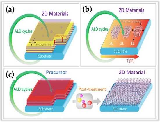
Figure 6. Schematic illustrations of three strategies for growth 2D materials via atomic layer deposition. Subfigure (a) represents method 1. Subfigure (b) represents method 2. Subfigure (c) represents method 3. Reprinted with permission from Ref. [53]. Copyright 2020, Elsevier.
An example of PA-ALD used in 2D film deposition is the work of Zhang et al. [64]. They used benzene (C6H6) and H2 plasma at 400 °C as reactants and co-reactant, respectively, in the deposition of graphene on Cu sheets. The authors suggested that the dehydrogenation process of benzene rings formed graphene. The method used was conventional ALD, and non-homogeneous graphene monolayers with grain size < 10 nm were grown below ten cycles. In contrast, ALD cycle values above ten led to high-quality, well-ordered multilayer graphene sheets.
Therefore, ALD 2D materials growth strategies expand the opportunities for 2D materials growth with high controllability, high quality, and large-scale production.
References
- Ziegler, J.; Mews, M.; Kaufmann, K.; Schneider, T.; Sprafke, A.N.; Korte, L.; Wehrspohn, R.B. Plasma-enhanced atomic-layer-deposited MoOx emitters for silicon heterojunction solar cells. Appl. Phys. A 2015, 120, 811–816.
- Garud, S.; Gampa, N.; Allen, T.G.; Kotipalli, R.; Flandre, D.; Batuk, M.; Hadermann, J.; Meuris, M.; Poortmans, J.; Smets, A.; et al. Surface passivation of CIGS solar cells using gallium oxide. Phys. Status Solidi A 2018, 215, 1700826.
- Ghods, A.; Saravade, V.G.; Zhou, C.; Ferguson, I.T. Field-effect passivation of metal/n-GaAs Schottky junction solar cells using atomic layer deposited Al2O3/ZnO ultrathin films. J. Vac. Sci. Technol. A 2020, 38, 012406.
- Koushik, D.; Jost, M.; Ducinskas, A.; Burgess, C.; Zardetto, V.; Weijtens, C.; Verheijen, M.A.; Kessels, W.M.M.; Albrecht, S.; Creatore, M. Plasma-assisted atomic layer deposition of nickel oxide as hole transport layer for hybrid perovskite solar cells. J. Mater. Chem. C 2019, 7, 12532–12543.
- Imai, T.; Mori, Y.; Kanomata, K.; Miura, M.; Ahmmad, B.; Kubota, S.; Hirose, F. Room-temperature plasma enhanced atomic layer deposition of aluminum silicate and its application in dye-sensitized solar cells. J. Vac. Sci. Technol. A 2018, 36, 01A106.
- Potscavage, W.J.; Yoo, S.; Domercq, B.; Kippelen, B. Encapsulation of pentacene/C60 organic solar cells with Al2O3 deposited by atomic layer deposition. Appl. Phys. Lett. 2007, 90, 253511.
- Wei, H.; Qiu, P.; Peng, M.; Wu, Q.; Liu, S.; Na, Y.; He, Y.; Song, Y.; Zheng, X. Interface modification for high-efficient quantum dot sensitized solar cells using ultrathin aluminum nitride coating. Appl. Surf. Sci. 2019, 476, 608–614.
- Wang, C.; Zhao, D.; Grice, C.R.; Liao, W.; Yu, Y.; Cimaroli, A.; Shrestha, N.; Roland, P.J.; Chen, J.; Yu, Z.; et al. Low-temperature plasma-enhanced atomic layer deposition of tin oxide electron selective layers for highly efficient planar perovskite solar cells. J. Mater. Chem. A 2016, 4, 12080–12087.
- Reichel, C.; Reusch, M.; Kotula, S.; Granek, F.; Richter, A.; Hermle, M.; Glunz, S.W. Insulating and passivating plasma-enhanced atomic layer deposited aluminum oxide thin films for silicon solar cells. Thin Solid Films 2018, 656, 53–60.
- Wang, H.; Zhao, Y.; Wang, Z.; Liu, Y.; Zhao, Z.; Xu, G.; Han, T.-H.; Lee, J.-W.; Chen, C.; Bao, D.; et al. Hermetic seal for perovskite solar cells: An improved plasma enhanced atomic layer deposition encapsulation. Nano Energy 2020, 69, 104375.
- Wang, D.; Wright, M.; Elumalai, N.K.; Uddin, A. Stability of perovskite solar cells. Sol. Energy Mater. Sol. Cells 2016, 147, 255–275.
- Han, T.-H.; Lee, Y.; Choi, M.-R.; Woo, S.-H.; Bae, S.-H.; Hong, B.H.; Ahn, J.-H.; Lee, T.-W. Extremely efficient flexible organic light-emitting diodes with modified graphene anode. Nat. Photonics 2012, 6, 105–110.
- Aziz, H.; Popovic, Z.; Xie, S.; Hor, A.-M.; Hu, N.-X.; Tripp, C.; Xu, G. Humidity-induced crystallization of tris(8-hydroxyquinoline) aluminum layers in organic light-emitting devices. Appl. Phys. Lett. 1998, 72, 756.
- Hoffmann, L.; Theirich, D.; Hasselman, T.; Räupke, A.; Schlaman, D.; Riedl, T. Gas permeation barriers deposited by atmospheric pressure plasma enhanced atomic layer deposition. J. Vac. Sci. Technol. A 2016, 34, 01A114.
- Kim, L.H.; Jeong, Y.J.; An, T.K.; Park, S.; Jang, J.H.; Nam, S.; Jang, J.; Kim, S.H.; Park, C.E. Optimization of Al2O3/TiO2 nanolaminates thin films prepared with different oxide ratios, for use in organic light-emitting diode encapsulation, via plasma-enhanced atomic layer deposition. Phys. Chem. Chem. Phys. 2016, 18, 1042.
- Jing, Y.; Merkx, J.M.; Cai, J.; Cao, K.; Kessels, W.M.M.; Mackus, J.M.; Chen, R. Nanoscale encapsulation of perovskite nanocrystal luminescent films via plasma-enhanced SiO2 atomic layer deposition. ACS Appl. Mater. Interfaces 2020, 12, 53519–53527.
- Yeom, H.-I.; Ko, J.B.; Mun, G.; Park, S.-H.K. High mobility polycrystalline indium oxide thin-film transistors by means of plasma-enhanced atomic layer deposition. J. Mater. Chem. C 2016, 4, 6873–6880.
- Egorov, K.V.; Kuzmichev, D.S.; Chizhov, P.S.; Lebedinskii, Y.Y.; Hwang, C.S.; Markeev, A.M. In situ control of oxygen vacancies in TaOx thin films via plasma-enhanced atomic layer deposition for resistive switching memory applications. ACS Appl. Mater. Interfaces 2017, 9, 13286–13292.
- Jha, R.K.; Singh, P.; Goswami, M.; Singh, B.R. Plasma enhanced atomic layer deposition HfO2 ferroelectric films for non-volatile memory applications. J. Electron. Mater. 2020, 49, 1445–1453.
- Henning, A.; Bartl, J.D.; Zeidler, A.; Qian, S.; Bienek, O.; Jiang, C.-M.; Paulus, C.; Rieger, B.; Stutzmann, M.; Sharp, I.D. Aluminum oxide at the monolayer limit via oxidant-free plasma-assisted atomic layer deposition on GaN. Adv. Funct. Mater. 2021, 31, 2101441.
- Xiao, Z.; Kisslinger, K.; Chance, S.; Banks, S. Comparison of hafnium dioxide and zirconium dioxide by plasma-enhanced atomic layer deposition for the application of electronic materials. Crystals 2020, 10, 136.
- Otto, L.M.; Hammack, A.T.; Aloni, S.; Ogletree, D.F.; Olynick, L.; Dhuey, S.; Stadler, J.H.; Schwartzberg, A.M. Plasma-enhanced atomic layer deposition for plasmonic TiN. Proc. SPIE 2016, 9919, 99190N.
- Krylov, I.; Zoubenko, E.; Weinfeld, K.; Kauffman, Y.; Xu, X.; Ritter, D.; Eizenberg, M. Obtaining low resitivity (~100 uW cm) TiN films by plasma enhanced atomic layer deposition using a metalorganic precursor. J. Vac. Sci. Technol. 2018, 36, 051505.
- Kim, H.; Song, H.; Shin, C.; Kim, K.; Jang, W.; Kim, H.; Shin, S.; Jeon, H. Dielectric barrier characteristics of Si-rich silicon nitride films deposited by plasma atomic layer deposition. J. Vac. Sci. Technol. 2017, 35, 01A101-1.
- Seppänen, H.; Kim, I.; Etula, J.; Ubyivovk, E.; Bouravleuv, A.; Lipsanen, H. Aluminum nitride transition layer for power electronics applications grown by plasma-enhanced atomic layer deposition. Materials 2019, 12, 406.
- Han, J.H.; Kim, H.Y.; Lee, S.C.; Kim, D.H.; Park, B.K.; Park, J.-S.; Jeon, D.J.; Chung, T.-M.; Kim, C.G. Growth of tantalum nitride film as a Cu diffusion barrier by plasma-enhanced atomic layer deposition from bis((2-(dimethylamino)ethyl)(methyl)amido)methyl(tert-butylimido)tantalum complex. Appl. Surf. Sci. 2016, 362, 176–181.
- Wang, X.-Z.; Muneshwar, T.P.; Fan, H.-Q.; Cadien, K.; Luo, J.-L. Achieving ultrahigh corrosion resistance and conductive zirconium oxynitride coating on metal bipolar plates by plasma enhanced atomic layer deposition. J. Power Sources 2018, 397, 32–36.
- Sowa, M.J.; Yemane, Y.; Zhang, J.; Palmstrom, J.C.; Ju, L.; Strandwitz, N.C.; Prinz, F.B.; Provine, J. Plasma-enhanced atomic layer deposition of superconducting niobium nitride. J. Vac. Sci. Technol. A 2017, 35, 01B143.
- Tian, L.; Bottala-Gambetta, I.; Marchetto, V.; Jacquemin, M.; Crisci, A.; Reboud, R.; Mantoux, A.; Berthomé, G.; Mercier, F.; Sulpice, A.; et al. Improved critical temperature of superconducting plasma-enhanced atomic layer deposition of niobium nitride thin films by thermal annealing. Thin Solid Films 2020, 709, 138232.
- Di Bartolomeo, A. Emerging 2D materials and their Van der Waals heterostructures. Nanomaterials 2020, 10, 579.
- Groven, B.; Heyne, M.; Mehta, A.N.; Bender, H.; Nuytten, T.; Meersschaut, J.; Conard, T.; Verdock, P.; Elshocht, S.V.; Vandervorst, W.; et al. Plasma-enhanced atomic layer deposition of two-dimensional WS2 from WF6, H2 plasma, and H2S. Chem. Mater. 2017, 29, 2927–2938.
- Balasubramanyam, S.; Shirazi, M.; Bloodgood, M.A.; Wu, L.; Verheijen, M.A.; Vandalon, V.; Kessels, W.M.M.; Hofmann, J.P.; Bol, A.A. Edge-site nanoengineering of WS2 by low-temperature plasma-enhanced atomic layer deposition for electrocatalytic hydrogen evolution. Chem. Mater. 2019, 31, 5104–5115.
- Sharma, A.; Verheijen, A.; Wu, L.; Karwal, S.; Vandalon, V.; Knoops, H.C.M.; Sundaram, R.S.; Hofmann, J.P.; Kessels, W.M.M.; Bol, A.A. Low-temperature plasma-enhanced atomic layer deposition of 2D MoS2: Large area, thickness control and tunable morphology. Nanoscale 2018, 10, 8615–8627.
- Vandalon, V.; Verheijen, M.A.; Kessels, W.M.M.; Bol, A.A. Atomic layer deposition of Al doped MoS: Synthesizing a p-type 2D semiconductor with tunable carrier density. ACS Appl. Nano Mater. 2020, 3, 10200–10208.
- Chiappim Júnior, W.; Moreno, L.X.; Pessoa, R.S.; da Cunha, A.F.; Salomé, P.M.P.; Leitão, J.P. Novel Dielectrics Compounds Grown by Atomic Layer Deposition as Sustainable Materials for Chalcogenides Thin Films Photovoltaics Technologies. In Sustainable Materials Solutions for Solar Energy Technologies: Processing Techniques and Applications, 1st ed.; Fraga, M.A., Amos, D., Sonmezoglu, S., Subramaniam, V., Eds.; Elsevier: Amsterdam, The Netherlands, 2021; Volume 1, pp. 71–100.
- Bugot, C.; Bouttemy, M.; Schneider, N.; Etcheberry, A.; Lincot, D.; Donsanti, F. New insights on the chemistry of plasma-enhanced atomic layer deposition of indium oxysulfide thin films and their use as buffer layers in Cu(In,Ga)Se2 thin film solar cell. J. Vac. Sci. Technol. 2018, 36, 061510.
- Wang, H.; Song, S.; Song, Z.; Zhou, Z.; Yao, D.; Lv, S. Fast and scalable phase change materials Ti-Sb-Te deposited by plasma-enhanced atomic layer deposition. J. Mater. Sci. Mater. Electron. 2020, 31, 5833–5837.
- Giordano, M.C.; Baumgaertl, K.; Steinvall, S.E.; Vuichard, M.; Fontcuberta i Morral, A.; Grundler, D. Plasma-enhanced atomic layer deposition of nickel nanotubes with low resistivity and coherent magnetization dynamics for 3D spintronics. ACS Appl. Mater. Interfaces 2020, 12, 40443–40452.
- Chiper, A.S. Tailoring the working gas flow to improve the surface modification of plasma-treated polymer. Mat. Lett. 2021, 305, 130832.
- Levchenko, I.; Xu, S.; Baranov, O.; Bazaka, O.; Ivanova, E.P.; Bazaka, K. Plasma and Polymers: Recent progress and trends. Molecules 2021, 26, 4091.
- Parsons, G.N.; Atasanov, S.E.; Dandley, E.C.; Devine, C.K.; Gong, B.; Jur, J.S.; Lee, K.; Oldham, C.J.; Peng, Q.; Spagnola, J.C.; et al. Mechanism and reactions during atomic layer deposition on polymers. Coord. Chem. Rev. 2013, 257, 3323–3331.
- Kim, G.H.; Lee, J.G.; Kim, S.S. Surface modification of polymeric substrates to enhance the barrier properties of an Al2O3 layer formed by PEALD. Org. Electron. 2017, 50, 239–246.
- Kääriäinen, T.O.; Lehti, S.; Kääriäinen, M.-L.; Cameron, D.C. Surface modification of polymers by plasma-assisted atomic layer deposition. Surf. Coat. Technol. 2011, 205, S475–S479.
- Cho, S.-W.; Jeong, J.-A.; Bae, J.-H.; Moon, J.-M.; Choi, K.-H.; Jeong, S.W.; Park, N.-J.; Kim, J.-J.; Lee, S.H.; Kang, J.-W.; et al. Highly flexible, transparent, and low resistance indium zinc oxide-Ag-indium zinc oxide multilayer anode on polyethylene terephthalate substrate for flexible organic light light-emitting diodes. Thin Solid Films 2008, 516, 7881–7885.
- Rahy, A.; Bajaj, P.; Musselman, I.H.; Hong, S.H.; Sun, Y.-P.; Yang, D.J. Coating of carbon nanotubes on flexible substrate and its adhesion study. Appl. Surf. Sci. 2009, 255, 7084–7089.
- Choi, M.-C.; Kim, Y.; Ha, C.-S. Polymers for flexible displays: From material selection to device applications. Prog. Polym. Sci. 2008, 33, 581–630.
- Fang, M.; Zhang, H.; Sang, L.; Cao, H.; Yang, L.; Ostrikov, K.; Levchenko, I.; Chen, Q. Plasma-assisted ALD to functionalize PET: Towards new generation flexible gadgets. Flex. Print. Electron. 2017, 2, 022001.
- Lee, Y.; Seo, S.; Oh, I.-K.; Lee, S.; Kim, H. Effects of O2 plasma treatment on moisture barrier properties of SiO2 grown by plasma-enhanced atomic layer deposition. Ceram. Int. 2019, 45, 17662–17668.
- Kovács, R.L.; Gyöngyösi, S.; Langer, G.; Baradács, E.; Daróczi, L.; Barkóczy, P.; Erdélyi, Z. Effect of nanoscopic defects on barrier performance of thin films deposited by plasma-enhanced atomic layer deposition on flexible polymers. Thin Solid Films 2021, 738, 138960.
- Sun, C.; Zhang, J.; Zhang, Y.; Zhao, F.; Xie, J.; Liu, Z.; Zhuang, J.; Zhang, N.; Ren, W.; Ye, Z.-G. Design and fabrication of flexible strain sensor based on ZnO-decorated PVDF via atomic layer deposition. Appl. Surf. Sci. 2021, 562, 150126.
- Cai, J.; Han, X.; Wang, X.; Meng, X. Atomic Layer Deposition of Two-Dimensional Layered Materials: Processes, Growth Mechanisms, and Characteristics. Matter 2020, 2, 587–630.
- Haider, A.; Ozgit-Akgun, C.; Goldenberg, E.; Okyay, A.K.; Biyikli, N. Low-Temperature Deposition of Hexagonal Boron Nitride via Sequential Injection of Triethylboron and N2/H2 Plasma. J. Am. Ceram. 2014, 97, 4052–4059.
- Park, H.; Kim, T.K.; Cho, S.W.; Jang, H.S.; Lee, S.I.; Choi, S.-Y. Large-scale synthesis of uniform hexagonal boron nitride films by plasma-enhanced atomic layer deposition. Sci. Rep. 2017, 7, 40091.
- Kim, Y.; Song, J.-G.; Park, Y.J.; Ryu, G.H.; Lee, S.J.; Kim, J.S.; Jeon, P.J.; Lee, C.W.; Woo, W.J.; Choi, T.; et al. Self-Limiting Layer Synthesis of Transition Metal Dichalcogenides. Sci. Rep. 2016, 4, 18754.
- Park, K.; Kim, Y.; Song, J.-G.; Kim, S.J.; Lee, C.W.; Ryu, G.H.; Lee, Z.; Park, J.; Kim, H. Uniform, large-area self-limiting layer synthesis of tungsten diselenide. 2D Materials 2016, 3, 014004.
- Martella, C.; Melloni, P.; Cinquanta, E.; Cianci, E.; Alia, M.; Longo, M.; Lamperti, A.; Vangelista, S.; Fanciulli, M.; Molle, A. Engineering the Growth of MoS2 via Atomic Layer Deposition of Molybdenum Oxide Film Precursor. Adv. Electron. Mater. 2016, 2, 1600330.
- Keller, B.D.; Bertuch, A.; Provine, J.; Sundaram, G.; Ferralis, N.; Grossman, J.C. Process Control of Atomic Layer Deposition Molybdenum Oxide Nucleation and Sulfidation to Large-Area MoS2 Monolayers. Chem. Mater. 2017, 29, 2024–2032.
- Dai, T.-J.; Fan, X.-D.; Ren, Y.-X.; Hou, S.; Zhang, Y.-Y.; Qian, L.-X.; Li, Y.-R.; Liu, X.-Z. Layer-controlled synthesis of wafer-scale MoSe2 nanosheets for photodetector arrays. J. Mater. Sci. 2018, 53, 8436–8444.
- Song, J.-G.; Park, J.; Lee, W.; Choi, T.; Jung, H.; Lee, C.W.; Hwang, S.-W.; Myoung, J.M.; Jung, J.-H.; Kim, S.-H.; et al. Layer-Controlled, Wafer-Scale, and Conformal Synthesis of Tungsten Disulfide Nanosheets Using Atomic Layer Deposition. ACS Nano 2013, 7, 11333–11340.
- Zeng, W.; Feng, L.-P.; Su, J.; Pan, H.-x.; Liu, Z.-T. Layer-controlled and atomically thin WS2 films prepared by sulfurization of atomic-layer-deposited WO3 films. J. Alloys Compd. 2018, 745, 834–839.
- Liu, H.F.; Antwi, K.K.A.; Wang, Y.D.; Ong, L.T.; Chua, S.J.; Chi, D.Z. Atomic layer deposition of crystalline Bi2O3 thin films and their conversion into Bi2S3 by thermal vapor desulfurization. RSC Adv. 2014, 4, 58724–58731.
- Jang, B.; Yeo, S.; Kim, H.; Shin, B.; Kim, S.-H. Fabrication of single-phase SnS film by H2 annealing of amorphous SnSx prepared by atomic layer deposition. J. Vac. Sci. Technol. A 2017, 35, 031506.
- Hao, W.; Marichy, C.; Journet, C.; Brioude, A. A novel two-step ammonia-free atomic layer deposition approach for boron nitride. ChemNanoMat 2017, 3, 656–663.
- Zhang, Y.; Ren, W.; Jiang, Z.; Yang, S.; Jing, W.; Shi, P.; Wu, X.; Ye, Z.-G. Lowtemperature remote plasma-enhanced atomic layer deposition of graphene and characterization of its atomic-level structure. J. Mater. Chem. C 2014, 2, 7570–7574.
More
Information
Subjects:
Physics, Fluids & Plasmas
Contributors
MDPI registered users' name will be linked to their SciProfiles pages. To register with us, please refer to https://encyclopedia.pub/register
:
View Times:
1.7K
Revisions:
2 times
(View History)
Update Date:
19 Oct 2022
Table of Contents


Notice
You are not a member of the advisory board for this topic. If you want to update advisory board member profile, please contact office@encyclopedia.pub.
OK
Confirm
Only members of the Encyclopedia advisory board for this topic are allowed to note entries. Would you like to become an advisory board member of the Encyclopedia?
Yes
No
${ textCharacter }/${ maxCharacter }
Submit
Cancel
Back
Comments
${ item }
|
${ item.createdUser.fullName }
${ item.createdAt }
${ item.vote }
${ item.reply }
Delete
${ reply.createdUser.fullName }
${ reply.createdAt }
${ reply.vote }
Delete
There is no reply to this comment~
${ item.replyTextCharacter }/${ item.replyMaxCharacter }
Submit
Cancel
More
No more~
There is no comment~
${ textCharacter }/${ maxCharacter }
Submit
Cancel
${ selectedItem.replyTextCharacter }/${ selectedItem.replyMaxCharacter }
Submit
Cancel
Confirm
Are you sure to Delete?
Yes
No