Submitted Successfully!
To reward your contribution, here is a gift for you: A free trial for our video production service.
Thank you for your contribution! You can also upload a video entry or images related to this topic.
Version Summary Created by Modification Content Size Created at Operation
1 -- 2032 2022-10-17 11:26:08 |
2 Reference format revised. -39 word(s) 1993 2022-10-18 04:08:27 | |
3 Figure format revised. Meta information modification 1993 2022-10-18 04:09:42 |

Video Upload Options

Do you have a full video?

Confirm

Are you sure to Delete?
Cite
If you have any further questions, please contact Encyclopedia Editorial Office.
Sengupta, J.;  Hussain, C.M. Application of Graphene in Electronic Devices. Encyclopedia. Available online: https://encyclopedia.pub/entry/29675 (accessed on 08 May 2024).
Sengupta J,  Hussain CM. Application of Graphene in Electronic Devices. Encyclopedia. Available at: https://encyclopedia.pub/entry/29675. Accessed May 08, 2024.
Sengupta, Joydip, Chaudhery Mustansar Hussain. "Application of Graphene in Electronic Devices" Encyclopedia, https://encyclopedia.pub/entry/29675 (accessed May 08, 2024).
Sengupta, J., & Hussain, C.M. (2022, October 17). Application of Graphene in Electronic Devices. In Encyclopedia. https://encyclopedia.pub/entry/29675
Sengupta, Joydip and Chaudhery Mustansar Hussain. "Application of Graphene in Electronic Devices." Encyclopedia. Web. 17 October, 2022.
Application of Graphene in Electronic Devices
Edit

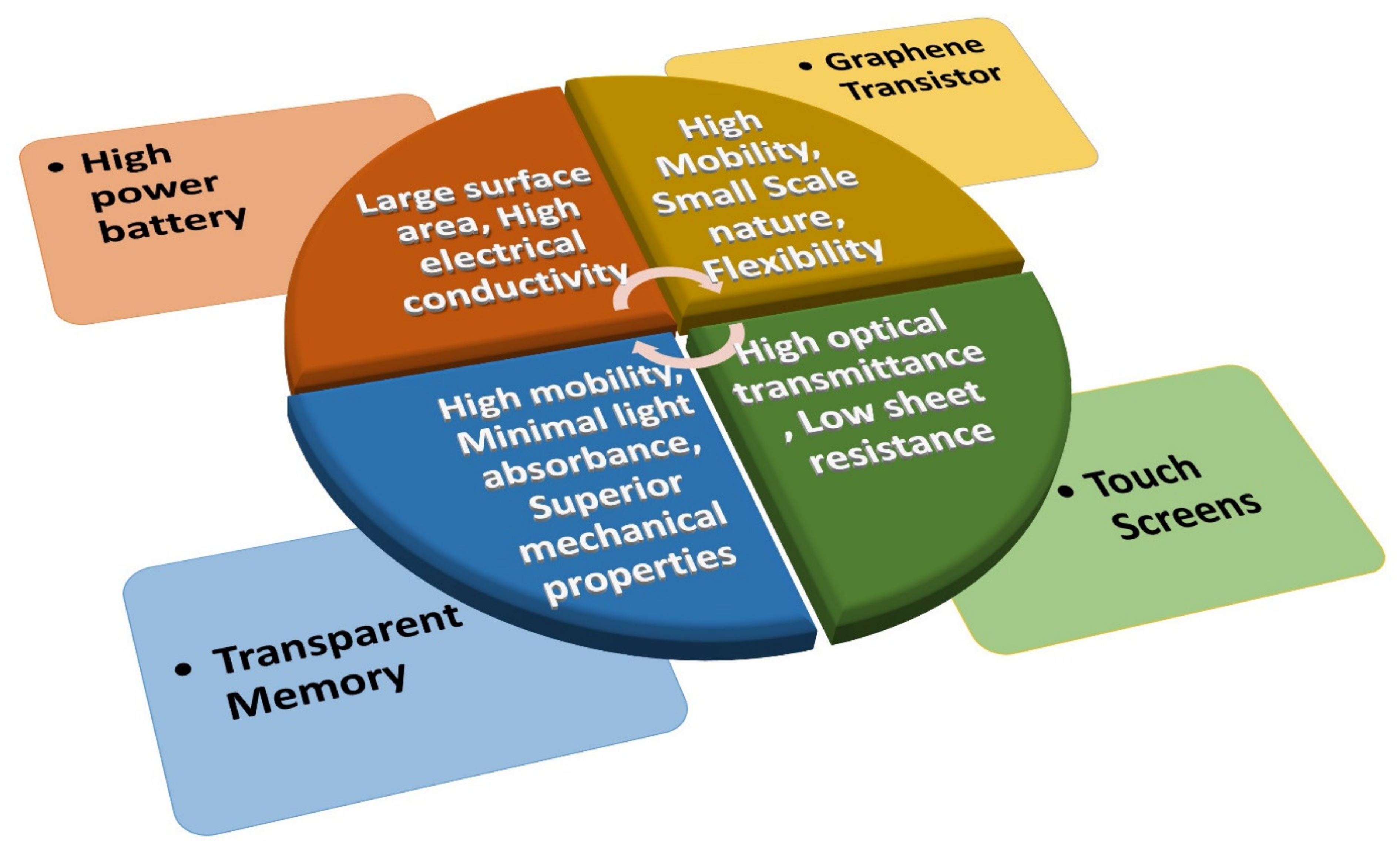
Graphene achieved a peerless level among nanomaterials in terms of its application in electronic devices, owing to its fascinating and novel properties. Its large surface area and high electrical conductivity combine to create high-power batteries. In addition, because of its high optical transmittance, low sheet resistance, and the possibility of transferring it onto plastic substrates, graphene is also employed as a replacement for indium tin oxide (ITO) in making electrodes for touch screens. Moreover, it was observed that graphene enhances the performance of transparent flexible electronic modules due to its higher mobility, minimal light absorbance, and superior mechanical properties. Graphene is even considered a potential substitute for the post-Si electronics era, where a high-performance graphene-based field-effect transistor (GFET) can be fabricated to detect the lethal SARS-CoV-2. Hence, graphene incorporation in electronic devices can facilitate immense device structure/performance advancements.

graphene nanomaterial electronics touch screen

1. Introduction

From a historical perspective, graphene was theoretically predicted as a part of graphite in the 1940s [1] and, in 1962, a single layer of graphite was first experimentally observed by Boehm et al. [2]. In 1994, Boehm coined the term “Graphene” [3]. Nearly two decades later, Novoselov et al. [4] reported, in the journal Science, the observation of graphene. Subsequently, graphene became the pivotal subject of research in the scientific community, which resulted in the rapid development of this field. The ultra-thin (0.35 nm) and super-light honeycomb configuration of graphene, with a planar density [5] of 0.77 mg/m2, captured great interest, owing to its novel nanostructure with unique physical and chemical properties [6]. In terms of crystal structure, graphene is the strongest material on earth [7], as well as being flexible [8]. This conclusion is based on the value of its Young’s modulus (1.0 terapascals), its intrinsic strength (130 gigapascals), and its breaking strength (42 N/m) [9]. Graphene exhibits supreme thermal conductivity [10], having a value up of to 8000 W/m·K [11], with a huge specific surface area of 2630 m2/g [12]. The transparency of graphene is another peerless feature, in that the transparency of a single layer of graphene is nearly 98% under visible light [13]. Its ultrahigh room-temperature electron mobility of 2 × 105 cm2V−1S−1 [14] established graphene as the most conductive material at room temperature to date, with a conductivity of 1.42 × 10⁶ S/m [15] and a sheet resistance of 125 Ω/sq [16]. Among these fascinating properties, some handpicked properties can be stitched together for specific applications in electronic devices, as shown in Scheme 1. The incorporation of graphene in electronic devices enhances their performance enormously.
/media/item_content/202210/634e07809e471nanomaterials-12-03146-sch001.png
Scheme 1. Mapping of graphene properties with potential applications in electronic devices.

2. Graphene Structure and Properties

Graphene is an atomically thin two-dimensional allotrope of carbon, comprising a single sheet of sp2-hybridized carbon atoms, where one atom forms each vertex. Here, the σ-bond is formed by the combination of S, Px, and the Py orbital, while the Pz orbital creates the π-bond. The π bond is mostly responsible for the large electrical conductivity of graphene [17].

There are three kinds of arrangements of carbon chain at the edge of graphene, namely zigzag, armchair, and arbitrary fashion, shown in Figure 1 (bottom left). The conduction behavior of graphene depends on the type of carbon chain arrangements at the edges. Zigzag arrangements of the carbon chain are responsible for metallic conduction, but a nanoribbon with armchair arrangements of the carbon chain acts either as a metal or a semiconductor [18]. Moreover, the bandgap of graphene nanoribbons varies inversely with the width of the nanoribbon [19]; this facilitates bandgap engineering for the potential application of graphene in nanoelectronic devices.
Moreover, graphene is so transparent that clear discrimination of single, bilayer, and multiple-layer graphene is possible by using contrast spectra; these can be generated from the reflection of a white light source from graphene, placed on an Si substrate with a 285 nm SiO2 capping layer [20]. Thus, theoretical and experimental results reveal that by varying the graphene thickness, the optical property of graphene can be controlled.
In the case of graphene, the first Brillouin zone contains four unique points in reciprocal space, including the Γ point at the center of the cell, K and K′ at inverse corners (Dirac points), and M at the edge center, the midpoint between K and K′. Monolayer graphene exhibits Dirac-type linear dispersion near EF = 0 due to its special hexagonal lattice structure.
Though graphene was first observed in the 1960s, exact nomenclature and proper classification remain a barrier to a precise definition of different forms of graphene, which acts as a hurdle for its standardization. To overcome this problem, several initiatives were undertaken across the globe. 
The fascinating features of graphene make it ideally suited for further miniaturizing electronics to form ultra-small devices and components for future semiconductor technology. However, for the practical realization of the potential of graphene, it must be synthesized in such a manner that the resulting product is almost defect-free. To date, several methods were devised to fabricate good quality graphene; these can be broadly categorized into top-down and bottom-up approaches. As the names suggest, in the case of the top-down approach, the initial material is a piece of graphite (in general) which is later reduced to single or few-layer graphene by various means (e.g., exfoliation etc.), whereas, in the case of the bottom-up approach, carbon molecules are assembled one by one (e.g., CVD etc.) to prepare a graphene layer. Moreover, a schematical description of different synthesis methods, quality of grown samples, and their target application fields are presented in Scheme 2.
/media/item_content/202210/634e080b3c03bnanomaterials-12-03146-sch002.png
Scheme 2. Mapping of graphene growth methods, product quality, and target applications in electronic devices.

3. Application of Graphene in Electronic Devices

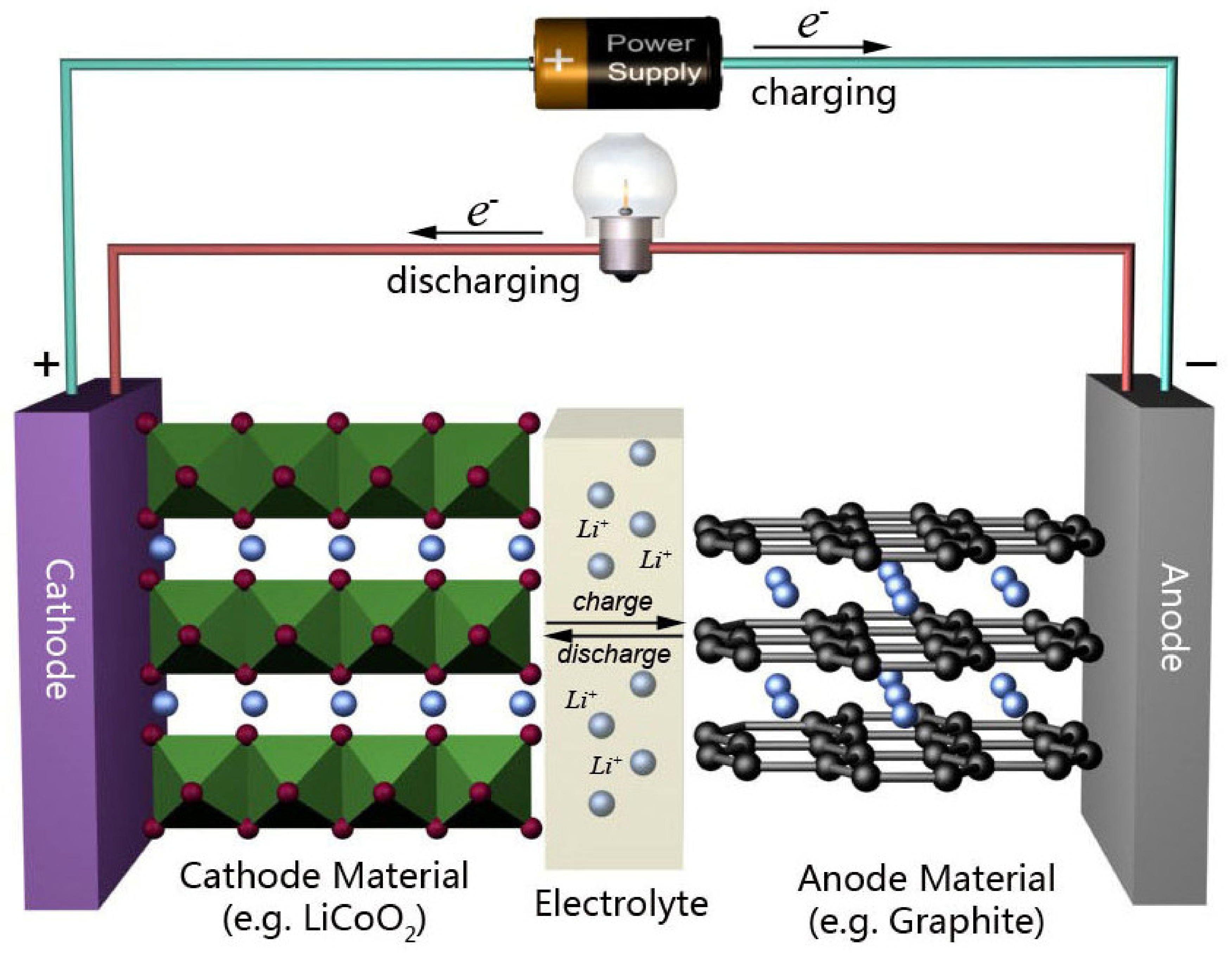
3.1. Graphene in Batteries

The battery, a device that converts chemical energy to electrical energy, is the utmost requirement for the smooth running of most daily-life hi-tech applications, for example, an electric razor. In the modern era, there is a need for a secondary-type battery that can be charged, discharged into a load, and recharged many times, as opposed to a primary-type battery, which is initially fully charged and must be discarded after use. A lightweight, durable secondary battery with a high energy-storage capacity, and a small charging time, is a prerequisite of modern electronic and electrical gadgets. Since the inception of research on secondary-type batteries [21], the lithium-ion battery (LIB) attracted major attention due to its unmatchable combination of high energy and power density (both gravimetric and volumetric) with long service life, environmental friendliness, and commercial viability [22]. However, continuous performance improvement is required for the sustainable development of any technology. A report [23] indicated that conduction is a key obstacle to the further upgrading of Li-ion batteries. In principle, the transport of Li ions between the anode and cathode materials, via the insertion/deintercalation process, is responsible for the charging and discharging of an LIB (Figure 1). The speed of transportation of Li ions between the electrodes through the electrolyte essentially determines the power capability of an LIB.
/media/item_content/202210/634e0909d2c72nanomaterials-12-03146-g005.png
Figure 1. The charge/discharge intercalation mechanism of Li-ion battery. (Reproduced with permission from ref [24]).
Thus, a nanostructure of a large surface area with high electrical conductivity is the key element for creating a high-power LIB. Graphene is the best-fit material to meet these requirements. However, the application of pristine graphene as the anode material presented a stability problem [25]. To circumvent this problem, hybrid materials were created and discovered to be useful for achieving battery enhancement. In the case of basic lithium-ion batteries, graphene can be incorporated either in the cathode or anode. Graphene and its derivatives, along with graphene-based composites, are used as anode materials in basic lithium-ion batteries.
Graphene and its derivatives, along with graphene-based composites, are also used as a cathode material in basic LIBs. Some of the most common cathode materials for LIBs are LiCoO2 [26], LiMn2O4 [27], LiFePO4 [28], Li3V2(PO4)3 [29], and V2O5 [30], owing to their high capacity, excellent cycle life, thermal stability, environmental benignity, and low cost. However, the low ionic and electrical conductivities of such cathode materials restrict their practical application. Here, graphene plays an important role as an electron-conducting additive for the above-mentioned substances and makes the resulting composite appreciably suitable as a cathode material. Deng et al. [31] used graphene as a conducting additive for LiCoO2 cathode materials and found that the surface wrinkles of graphene-wrapped LiCoO2 particles formed a plane-contacted interface which enhanced the conductivity of the cathode; the high-rate cycling stability was also improved. The experimental results showed that after 300 cycles, the capacity of a graphene/LiCoO2 battery decreased from 145 to 137.8 mAh/g, which was 95.1% of the initial discharging capacity. Pyun et al. [32] found that the discharge capacity, cyclic performance stability, and rate capability of the graphene/LiMn2O4 electrodes were significantly higher than those of the pristine LiMn2O4 electrodes. The scholars concluded that the high surface area of LiMn2O4 nanoparticles and good electronic conductivity of graphene were responsible for the enhanced performance. Hu et al. [33] modified the surface of LiFePO4 with 2 wt% of electrochemically exfoliated graphene layers, with the resulting composite being able to reach 208 mAh/g in specific capacity, which was beyond the theoretical capacity of 170 mAh/g. They also indicated that such a simple and scalable approach might also be applied to other cathode systems, boosting the capacity of various Li batteries.

3.2. Graphene Electrodes for Touch Screens

From the inception of the idea of the “touch screen” [34] to date, metal oxides [35] are primarily employed for its production. Among various metal oxides, ITO [36] is the most attractive, owing to its unique combination of visible light transparency and modest conductivity [37]. However, ITO is chemically unstable [38], expensive, and not flexible, and these drawbacks necessitate the search for a better substitute. Subsequently, diverse forms of materials, including nanomaterials [39] underwent feasibility tests in terms of cost, chemical stability, flexibility, transparency, and conductivity. Numerous studies [40][41] demonstrated that graphene had the potential to replace ITO because of its small sheet resistance, large optical transmittance, and the possibility of transferring it onto plastic substrates. Additionally, graphene-based transparent conductive electrodes can be produced on a large scale via the roll-to-roll technique to fabricate touch screens [42]. Even by combining the rod-coating technique and the room-temperature reduction in GO, it is possible to fabricate large-scale highly flexible rGO films directly on PET (polyethylene terephthalate) substrates [43], with low resistance and good transparency (~80%).

3.3. Transparent Memory with Graphene

The parametric measures of good electronic gadgets are changing rapidly. The inclusion of multiple functionalities, such as transparency, wearability, flexibility, portability, etc., are the prime aspects of advancement for today’s electronic gadgets, which is leading to a new era of electronic gadgets called “transparent electronics”. Semiconducting nanowires [44] made of wide bandgap semiconductors were initially employed for the fabrication of transparent electronics. It was later found that incorporation of graphene augments the performance of transparent–flexible electronic gadgets because of its finer mechanical properties, negligible light absorbance, and superior mobility. Moreover, because of the high density of states and large work functions with excellent electrical properties, graphene became a promising material for non-volatile transparent, flexible memory devices, in which it can be employed as a conducting channel or a charge-storing layer.

3.4. Integrated Circuits with Graphene Transistors

Currently, for the fabrication of integrated circuits, complementary metal oxide semiconductor (CMOS) technology is used. However, the advancement of fabrication technology is approaching the limits of downsizing transistors in a rapid manner [45]. Graphene can be considered a potential substitute for post-Si electronics [46]. However, the fabrication technology of graphene-based low-power devices is still in the development stage, and an improved growth technique to produce large-area graphene films with superior electrical properties on dielectric surfaces needs to be developed. Meanwhile, Lemme et al. [47] reported the fabrication of a top-gated field-effect device using monolayer graphene. The carrier mobility value exceeded the universal mobility in the silicon and ultrathin body SOI MOSFETs. However, the scholars suggested that bandgap tuning would be necessary to improve the device characteristics. Sun et al. [48] realized a double-gated GFET, with graphene as the working channel and organic ferroelectric sheets (PVDF-TrFE) as the top gating insulator. The inclusion of ferroelectric material substantially modified the charge transport properties in the graphene channels. The top-gate dielectrics isolated the graphene channels from the effects of the environment.

References

  1. Wallace, P.R. The Band Theory of Graphite. Phys. Rev. 1947, 71, 622–634.
  2. Boehm, H.P.; Clauss, A.; Fischer, G.O.; Hofmann, U. Dünnste Kohlenstoff-Folien. Z. Nat. B 1962, 17, 150–153.
  3. Boehm, H.P.; Setton, R.; Stumpp, E. Nomenclature and Terminology of Graphite Intercalation Compounds (IUPAC Recommendations 1994). Pure Appl. Chem. 1994, 66, 1893–1901.
  4. Novoselov, K.S.; Geim, A.K.; Morozov, S.V.; Jiang, D.; Zhang, Y.; Dubonos, S.V.; Grigorieva, I.V.; Firsov, A.A. Electric Field Effect in Atomically Thin Carbon Films. Science 2004, 306, 666–669.
  5. Li, Q.; Guo, B.D.; Yu, J.G.; Ran, J.R.; Zhang, B.H.; Yan, H.J.; Gong, J.R. Highly Efficient Visible-Light-Driven Photocatalytic Hydrogen Production of CdS-Cluster-Decorated Graphene Nanosheets. J. Am. Chem. Soc. 2011, 133, 10878–10884.
  6. Geim, A.K.; Novoselov, K.S. The Rise of Graphene. Nat. Mater. 2007, 6, 183–191.
  7. Lee, G.-H.; Cooper, R.C.; An, S.J.; Lee, S.; van der Zande, A.; Petrone, N.; Hammerberg, A.G.; Lee, C.; Crawford, B.; Oliver, W.; et al. High-Strength Chemical-Vapor-Deposited Graphene and Grain Boundaries. Science 2013, 340, 1073–1076.
  8. Vekeman, J.; Sánchez-Marín, J.; Sánchez de Merás, A.; Garcia Cuesta, I.; Faginas-Lago, N. Flexibility in the Graphene Sheet: The Influence on Gas Adsorption from Molecular Dynamics Studies. J. Phys. Chem. C 2019, 123, 28035–28047.
  9. Lee, C.; Wei, X.; Kysar, J.W.; Hone, J. Measurement of the Elastic Properties and Intrinsic Strength of Monolayer Graphene. Science 2008, 321, 385–388.
  10. Ghosh, S.; Calizo, I.; Teweldebrhan, D.; Pokatilov, E.P.; Nika, D.L.; Balandin, A.A.; Bao, W.; Miao, F.; Lau, C.N. Extremely High Thermal Conductivity of Graphene: Prospects for Thermal Management Applications in Nanoelectronic Circuits. Appl. Phys. Lett. 2008, 92, 151911.
  11. Pop, E.; Varshney, V.; Roy, A.K. Thermal Properties of Graphene: Fundamentals and Applications. MRS Bull. 2012, 37, 1273–1281.
  12. Stoller, M.D.; Park, S.; Yanwu, Z.; An, J.; Ruoff, R.S.; Zhu, Y.; An, J.; Ruoff, R.S.; Yanwu, Z.; An, J.; et al. Graphene-Based Ultracapacitors. Nano Lett. 2008, 8, 3498–3502.
  13. Nair, R.R.; Blake, P.; Grigorenko, A.N.; Novoselov, K.S.; Booth, T.J.; Stauber, T.; Peres, N.M.R.; Geim, A.K. Fine Structure Constant Defines Visual Transparency of Graphene. Science 2008, 320, 1308.
  14. Bolotin, K.I.; Sikes, K.J.; Jiang, Z.; Klima, M.; Fudenberg, G.; Hone, J.; Kim, P.; Stormer, H.L. Ultrahigh Electron Mobility in Suspended Graphene. Solid State Commun. 2008, 146, 351–355.
  15. Choi, J.S.; Choi, H.; Kim, K.C.; Jeong, H.Y.; Yu, Y.J.; Kim, J.T.; Kim, J.S.; Shin, J.W.; Cho, H.; Choi, C.G. Facile Fabrication of Properties-Controllable Graphene Sheet. Sci. Rep. 2016, 6, 24525.
  16. Bae, S.; Kim, H.; Lee, Y.; Xu, X.; Park, J.S.; Zheng, Y.; Balakrishnan, J.; Lei, T.; Ri Kim, H.; Song, Y.I.; et al. Roll-to-Roll Production of 30-Inch Graphene Films for Transparent Electrodes. Nat. Nanotechnol. 2010, 5, 574–578.
  17. Littlejohn, S.D. Electrical Properties of Graphite Nanoparticles in Silicone; Springer: Berlin/Heidelberg, Germany, 2014; ISBN 978-3-319-00740-3.
  18. Martin, I.; Blanter, Y.M. Transport in Disordered Graphene Nanoribbons. Phys. Rev. B 2009, 79, 235132.
  19. Son, Y.W.; Cohen, M.L.; Louie, S.G. Energy Gaps in Graphene Nanoribbons. Phys. Rev. Lett. 2006, 97, 216803.
  20. Ni, Z.H.; Wang, H.M.; Kasim, J.; Fan, H.M.; Yu, T.; Wu, Y.H.; Feng, Y.P.; Shen, Z.X.; About, M.; Article, T. Reflection and Contrast Spectroscopy Graphene Thickness Determination Using Reflection and Contrast Spectroscopy. Nano Lett. 2007, 7, 2758–2763.
  21. Vinal, G.W. Storage Batteries. J. Opt. Soc. Am. 1925, 11, 263–274.
  22. Lithium-Ion Batteries Need to Be Greener and More Ethical. Nature 2021, 595, 7.
  23. Hein, S.; Danner, T.; Westhoff, D.; Prifling, B.; Scurtu, R.; Kremer, L.; Hoffmann, A.; Hilger, A.; Osenberg, M.; Manke, I.; et al. Influence of Conductive Additives and Binder on the Impedance of Lithium-Ion Battery Electrodes: Effect of Morphology. J. Electrochem. Soc. 2020, 167, 013546.
  24. Liu, R.; Duay, J.; Lee, S.B. Heterogeneous Nanostructured Electrode Materials for Electrochemical Energy Storage. Chem Commun. 2011, 47, 1384–1404.
  25. Asenbauer, J.; Eisenmann, T.; Kuenzel, M.; Kazzazi, A.; Chen, Z.; Bresser, D. The Success Story of Graphite as a Lithium-Ion Anode Material—Fundamentals, Remaining Challenges, and Recent Developments Including Silicon (Oxide) Composites. Sustain. Energy Fuels 2020, 4, 5387–5416.
  26. Takahashi, Y.; Tode, S.; Kinoshita, A.; Fujimoto, H.; Nakane, I.; Fujitani, S. Development of Lithium-Ion Batteries with a LiCoO Cathode Toward High Capacity by Elevating Charging Potential. J. Electrochem. Soc. 2008, 155, A537–A541.
  27. Lee, M.; Lee, S.; Oh, P.; Kim, Y.; Cho, J. High Performance LiMn2O4 Cathode Materials Grown with Epitaxial Layered Nanostructure for Li-Ion Batteries. Nano Lett. 2014, 14, 993–999.
  28. Zhang, Y.; Wang, C.Y.; Tang, X. Cycling Degradation of an Automotive LiFePO4 lithium-Ion Battery. J. Power Sources 2011, 196, 1513–1520.
  29. Gaubicher, J.; Wurm, C.; Goward, G.; Masquelier, C.; Nazar, L. Rhombohedral Form of Li3V2(PO4)3 as a Cathode in Li-Ion Batteries. Chem. Mater. 2000, 12, 3240–3242.
  30. Wang, S.; Lu, Z.; Wang, D.; Li, C.; Chen, C.; Yin, Y. Porous Monodisperse V2O5 Microspheres as Cathode Materials for Lithium-Ion Batteries. J. Mater. Chem. 2011, 21, 6365–6369.
  31. Deng, L.-F.; Yu, K.-M. Influence of Graphene on the Electrochemical Performance of LiCoO2 Cathode Materials for Lithium-Ion Batteries. J. Funct. Mater. 2014, 45, 84–88.
  32. Pyun, M.H.; Park, Y.J. Graphene/LiMn2O4 Nanocomposites for Enhanced Lithium Ion Batteries with High Rate Capability. J. Alloys Comp. 2015, 643, S90–S94.
  33. Lung-Hao Hu, B.; Wu, F.Y.; Lin, C.T.; Khlobystov, A.N.; Li, L.J. Graphene-Modified LiFePO4 Cathode for Lithium Ion Battery beyond Theoretical Capacity. Nat. Commun. 2013, 4, 1687.
  34. Johnson, E.A. Touch Display—A Novel Input/Output Device for Computers. Electron. Lett. 1965, 1, 219–220.
  35. Yu, X.; Marks, T.J.; Facchetti, A. Metal Oxides for Optoelectronic Applications. Nat. Mater. 2016, 15, 383–396.
  36. Hong, C.-H.; Shin, J.-H.; Ju, B.-K.; Kim, K.-H.; Park, N.-M.; Kim, B.-S.; Cheong, W.-S. Index-Matched Indium Tin Oxide Electrodes for Capacitive Touch Screen Panel Applications. J. Nanosci. Nanotechnol. 2013, 13, 7756–7759.
  37. Her, S.-C.; Chang, C.-F. Fabrication and Characterization of Indium Tin Oxide Films. J. Appl. Biomater. Funct. Mater. 2017, 15, 170–175.
  38. Geiger, S.; Kasian, O.; Mingers, A.M.; Mayrhofer, K.J.J.; Cherevko, S. Stability Limits of Tin-Based Electrocatalyst Supports. Sci. Rep. 2017, 7, 4595.
  39. Layani, M.; Kamyshny, A.; Magdassi, S. Transparent Conductors Composed of Nanomaterials. Nanoscale 2014, 6, 5581–5591.
  40. Arvidsson, R.; Kushnir, D.; Molander, S.; Sandén, B.A. Energy and Resource Use Assessment of Graphene as a Substitute for Indium Tin Oxide in Transparent Electrodes. J. Clean. Prod. 2016, 132, 289–297.
  41. Das, T.; Sharma, B.K.; Katiyar, A.K.; Ahn, J.-H. Graphene-Based Flexible and Wearable Electronics. J. Semicond. 2018, 39, 011007.
  42. Ryu, J.; Kim, Y.; Won, D.; Kim, N.; Park, J.S.; Lee, E. Fast Synthesis of High-Performance Graphene by Rapid Thermal Chemical Vapor Deposition. ACS Nano 2014, 8, 950–956.
  43. Wang, J.; Liang, M.; Fang, Y.; Qiu, T.; Zhang, J.; Zhi, L. Rod-Coating: Towards Large-Area Fabrication of Uniform Reduced Graphene Oxide Films for Flexible Touch Screens. Adv. Mater. 2012, 24, 2874–2878.
  44. Dong, T.; Sun, Y.; Zhu, Z.; Wu, X.; Wang, J.; Shi, Y.; Xu, J.; Chen, K.; Yu, L. Monolithic Integration of Silicon Nanowire Networks as a Soft Wafer for Highly Stretchable and Transparent Electronics. Nano Lett. 2019, 19, 6235–6243.
  45. Yoon, J.-S.; Lee, S.; Lee, J.; Jeong, J.; Yun, H.; Kang, B.; Baek, R.-H. Source/Drain Patterning FinFETs as Solution for Physical Area Scaling Toward 5-Nm Node. IEEE Access 2019, 7, 172290–172295.
  46. Lu, H.-W.; Kane, A.A.; Parkinson, J.; Gao, Y.; Hajian, R.; Heltzen, M.; Goldsmith, B.; Aran, K. The Promise of Graphene-Based Transistors for Democratizing Multiomics Studies. Biosens. Bioelectron. 2022, 195, 113605.
  47. Lemme, M.C.; Member, S.; Echtermeyer, T.J.; Baus, M.; Kurz, H. A Graphene Field-Effect Device. IEEE Electron. Dev. Lett. 2007, 28, 282–284.
  48. Sun, Y.-L.; Xie, D.; Xu, J.-L.; Li, X.-M.; Zhang, C.; Dai, R.-X.; Li, X.; Meng, X.-J.; Zhu, H.-W. Tunable Transport Characteristics of Double-Gated Graphene Field-Effect Transistors Using P(VDF-TrFE) Ferroelectric Gating. Carbon 2016, 96, 695–700.
More
Information
Contributors MDPI registered users' name will be linked to their SciProfiles pages. To register with us, please refer to https://encyclopedia.pub/register : ,
View Times: 1.4K
Revisions: 3 times (View History)
Update Date: 18 Oct 2022
1000/1000