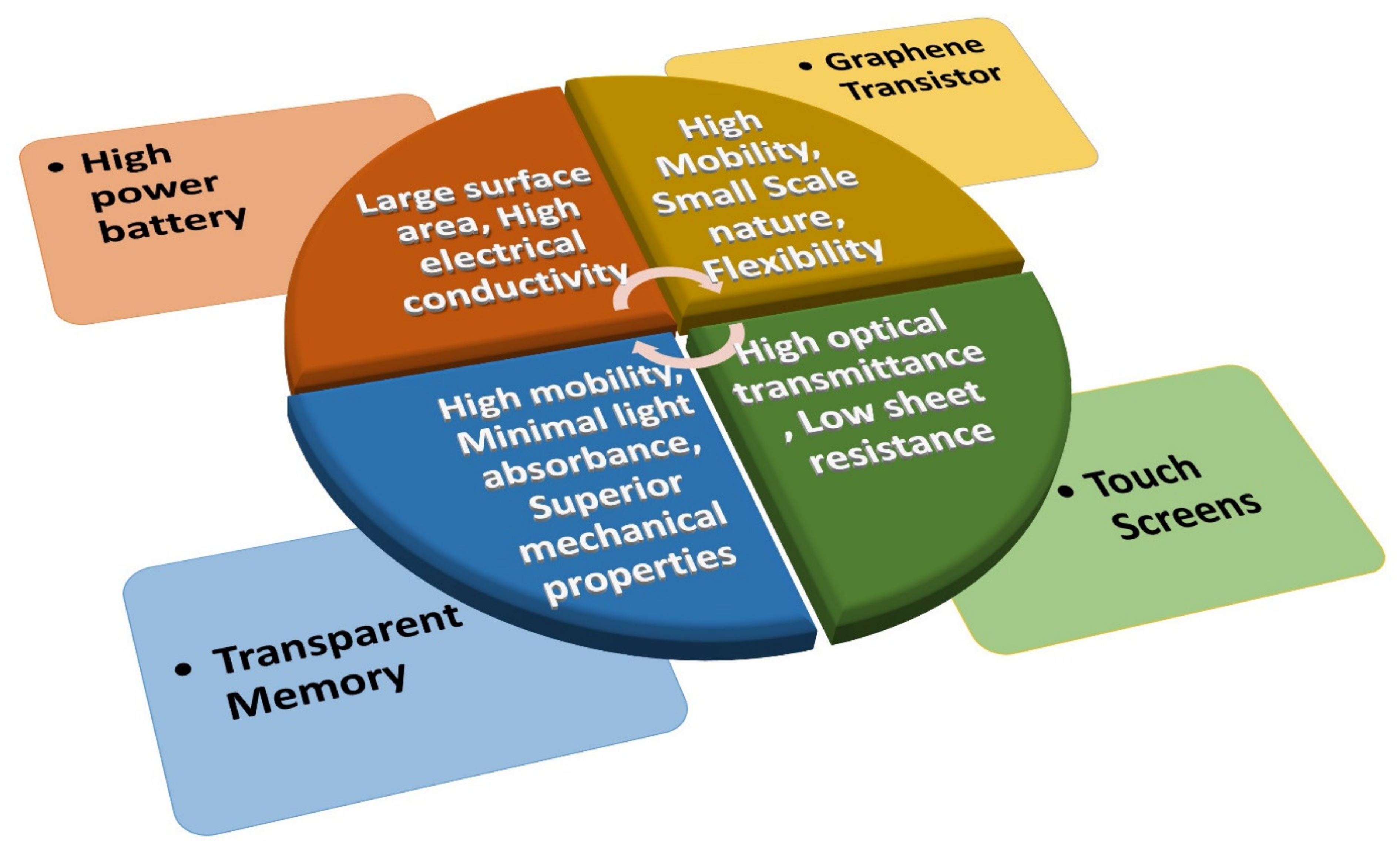
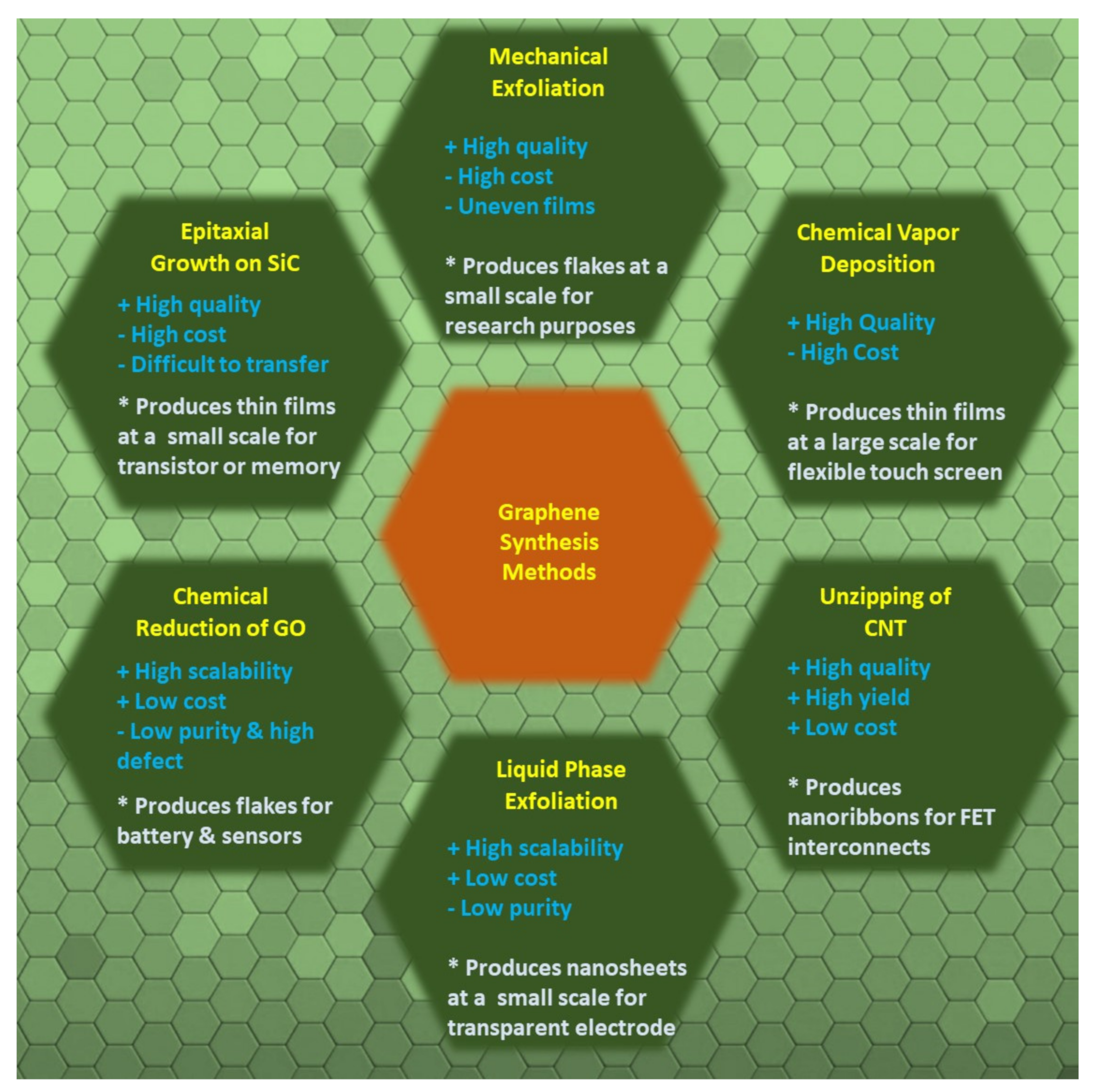
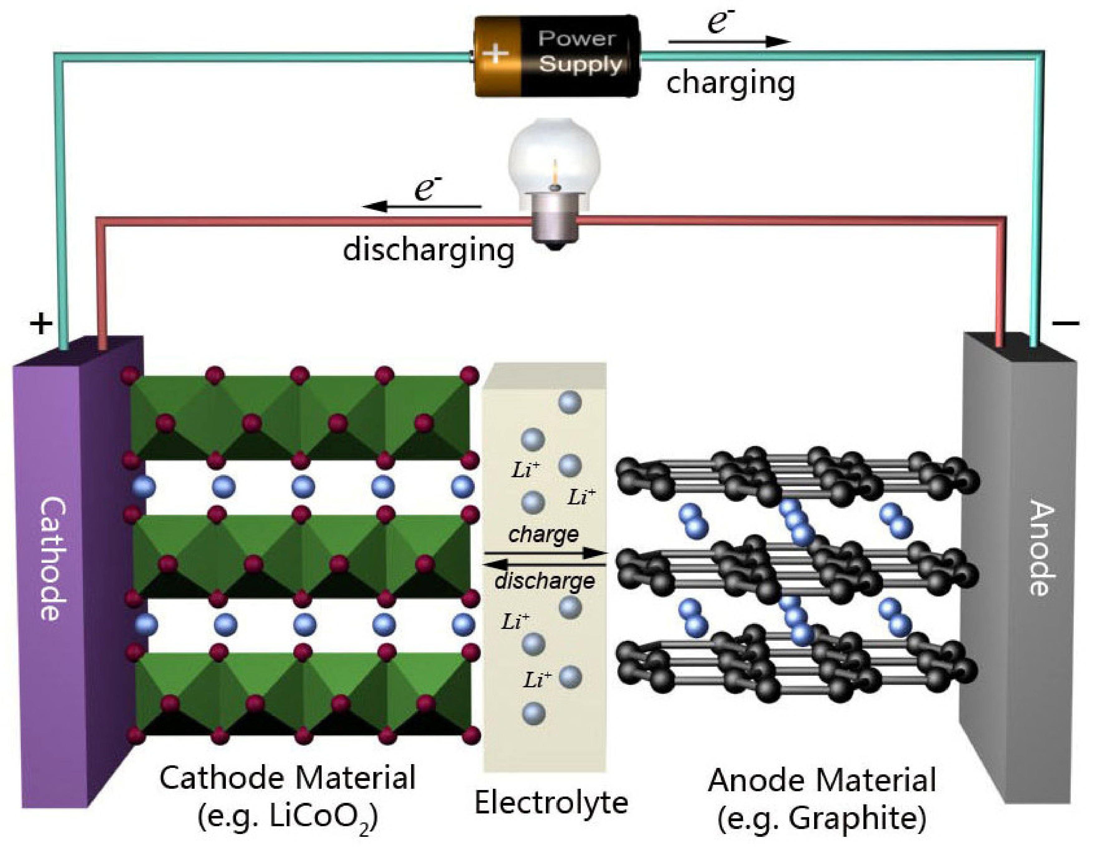
Graphene achieved a peerless level among nanomaterials in terms of its application in electronic devices, owing to its fascinating and novel properties. Its large surface area and high electrical conductivity combine to create high-power batteries. In addition, because of its high optical transmittance, low sheet resistance, and the possibility of transferring it onto plastic substrates, graphene is also employed as a replacement for indium tin oxide (ITO) in making electrodes for touch screens. Moreover, it was observed that graphene enhances the performance of transparent flexible electronic modules due to its higher mobility, minimal light absorbance, and superior mechanical properties. Graphene is even considered a potential substitute for the post-Si electronics era, where a high-performance graphene-based field-effect transistor (GFET) can be fabricated to detect the lethal SARS-CoV-2. Hence, graphene incorporation in electronic devices can facilitate immense device structure/performance advancements.
- graphene
- nanomaterial
- electronics
- touch screen
1. Introduction

2. Graphene Structure and Properties
Graphene is an atomically thin two-dimensional allotrope of carbon, comprising a single sheet of sp2-hybridized carbon atoms, where one atom forms each vertex. Here, the σ-bond is formed by the combination of S, Px, and the Py orbital, while the Pz orbital creates the π-bond. The π bond is mostly responsible for the large electrical conductivity of graphene [17].

3. Application of Graphene in Electronic Devices
3.1. Graphene in Batteries

3.2. Graphene Electrodes for Touch Screens
From the inception of the idea of the “touch screen” [97][34] to date, metal oxides [98][35] are primarily employed for its production. Among various metal oxides, ITO [99][36] is the most attractive, owing to its unique combination of visible light transparency and modest conductivity [100][37]. However, ITO is chemically unstable [101][38], expensive, and not flexible, and these drawbacks necessitate the search for a better substitute. Subsequently, diverse forms of materials, including nanomaterials [102][39] underwent feasibility tests in terms of cost, chemical stability, flexibility, transparency, and conductivity. Numerous studies [103,104][40][41] demonstrated that graphene had the potential to replace ITO because of its small sheet resistance, large optical transmittance, and the possibility of transferring it onto plastic substrates. Additionally, graphene-based transparent conductive electrodes can be produced on a large scale via the roll-to-roll technique to fabricate touch screens [105][42]. Even by combining the rod-coating technique and the room-temperature reduction in GO, it is possible to fabricate large-scale highly flexible rGO films directly on PET (polyethylene terephthalate) substrates [106][43], with low resistance and good transparency (~80%).3.3. Transparent Memory with Graphene
The parametric measures of good electronic gadgets are changing rapidly. The inclusion of multiple functionalities, such as transparency, wearability, flexibility, portability, etc., are the prime aspects of advancement for today’s electronic gadgets, which is leading to a new era of electronic gadgets called “transparent electronics”. Semiconducting nanowires [120][44] made of wide bandgap semiconductors were initially employed for the fabrication of transparent electronics. It was later found that incorporation of graphene augments the performance of transparent–flexible electronic gadgets because of its finer mechanical properties, negligible light absorbance, and superior mobility. Moreover, because of the high density of states and large work functions with excellent electrical properties, graphene became a promising material for non-volatile transparent, flexible memory devices, in which it can be employed as a conducting channel or a charge-storing layer.3.4. Integrated Circuits with Graphene Transistors
Currently, for the fabrication of integrated circuits, complementary metal oxide semiconductor (CMOS) technology is used. However, the advancement of fabrication technology is approaching the limits of downsizing transistors in a rapid manner [133][45]. Graphene can be considered a potential substitute for post-Si electronics [134][46]. However, the fabrication technology of graphene-based low-power devices is still in the development stage, and an improved growth technique to produce large-area graphene films with superior electrical properties on dielectric surfaces needs to be developed. Meanwhile, Lemme et al. [135][47] reported the fabrication of a top-gated field-effect device using monolayer graphene. The carrier mobility value exceeded the universal mobility in the silicon and ultrathin body SOI MOSFETs. However, the autscholars suggested that bandgap tuning would be necessary to improve the device characteristics. Sun et al. [136][48] realized a double-gated GFET, with graphene as the working channel and organic ferroelectric sheets (PVDF-TrFE) as the top gating insulator. The inclusion of ferroelectric material substantially modified the charge transport properties in the graphene channels. The top-gate dielectrics isolated the graphene channels from the effects of the environment.References
- Wallace, P.R. The Band Theory of Graphite. Phys. Rev. 1947, 71, 622–634.
- Boehm, H.P.; Clauss, A.; Fischer, G.O.; Hofmann, U. Dünnste Kohlenstoff-Folien. Z. Nat. B 1962, 17, 150–153.
- Boehm, H.P.; Setton, R.; Stumpp, E. Nomenclature and Terminology of Graphite Intercalation Compounds (IUPAC Recommendations 1994). Pure Appl. Chem. 1994, 66, 1893–1901.
- Novoselov, K.S.; Geim, A.K.; Morozov, S.V.; Jiang, D.; Zhang, Y.; Dubonos, S.V.; Grigorieva, I.V.; Firsov, A.A. Electric Field Effect in Atomically Thin Carbon Films. Science 2004, 306, 666–669.
- Li, Q.; Guo, B.D.; Yu, J.G.; Ran, J.R.; Zhang, B.H.; Yan, H.J.; Gong, J.R. Highly Efficient Visible-Light-Driven Photocatalytic Hydrogen Production of CdS-Cluster-Decorated Graphene Nanosheets. J. Am. Chem. Soc. 2011, 133, 10878–10884.
- Geim, A.K.; Novoselov, K.S. The Rise of Graphene. Nat. Mater. 2007, 6, 183–191.
- Lee, G.-H.; Cooper, R.C.; An, S.J.; Lee, S.; van der Zande, A.; Petrone, N.; Hammerberg, A.G.; Lee, C.; Crawford, B.; Oliver, W.; et al. High-Strength Chemical-Vapor-Deposited Graphene and Grain Boundaries. Science 2013, 340, 1073–1076.
- Vekeman, J.; Sánchez-Marín, J.; Sánchez de Merás, A.; Garcia Cuesta, I.; Faginas-Lago, N. Flexibility in the Graphene Sheet: The Influence on Gas Adsorption from Molecular Dynamics Studies. J. Phys. Chem. C 2019, 123, 28035–28047.
- Lee, C.; Wei, X.; Kysar, J.W.; Hone, J. Measurement of the Elastic Properties and Intrinsic Strength of Monolayer Graphene. Science 2008, 321, 385–388.
- Ghosh, S.; Calizo, I.; Teweldebrhan, D.; Pokatilov, E.P.; Nika, D.L.; Balandin, A.A.; Bao, W.; Miao, F.; Lau, C.N. Extremely High Thermal Conductivity of Graphene: Prospects for Thermal Management Applications in Nanoelectronic Circuits. Appl. Phys. Lett. 2008, 92, 151911.
- Pop, E.; Varshney, V.; Roy, A.K. Thermal Properties of Graphene: Fundamentals and Applications. MRS Bull. 2012, 37, 1273–1281.
- Stoller, M.D.; Park, S.; Yanwu, Z.; An, J.; Ruoff, R.S.; Zhu, Y.; An, J.; Ruoff, R.S.; Yanwu, Z.; An, J.; et al. Graphene-Based Ultracapacitors. Nano Lett. 2008, 8, 3498–3502.
- Nair, R.R.; Blake, P.; Grigorenko, A.N.; Novoselov, K.S.; Booth, T.J.; Stauber, T.; Peres, N.M.R.; Geim, A.K. Fine Structure Constant Defines Visual Transparency of Graphene. Science 2008, 320, 1308.
- Bolotin, K.I.; Sikes, K.J.; Jiang, Z.; Klima, M.; Fudenberg, G.; Hone, J.; Kim, P.; Stormer, H.L. Ultrahigh Electron Mobility in Suspended Graphene. Solid State Commun. 2008, 146, 351–355.
- Choi, J.S.; Choi, H.; Kim, K.C.; Jeong, H.Y.; Yu, Y.J.; Kim, J.T.; Kim, J.S.; Shin, J.W.; Cho, H.; Choi, C.G. Facile Fabrication of Properties-Controllable Graphene Sheet. Sci. Rep. 2016, 6, 24525.
- Bae, S.; Kim, H.; Lee, Y.; Xu, X.; Park, J.S.; Zheng, Y.; Balakrishnan, J.; Lei, T.; Ri Kim, H.; Song, Y.I.; et al. Roll-to-Roll Production of 30-Inch Graphene Films for Transparent Electrodes. Nat. Nanotechnol. 2010, 5, 574–578.
- Littlejohn, S.D. Electrical Properties of Graphite Nanoparticles in Silicone; Springer: Berlin/Heidelberg, Germany, 2014; ISBN 978-3-319-00740-3.
- Martin, I.; Blanter, Y.M. Transport in Disordered Graphene Nanoribbons. Phys. Rev. B 2009, 79, 235132.
- Son, Y.W.; Cohen, M.L.; Louie, S.G. Energy Gaps in Graphene Nanoribbons. Phys. Rev. Lett. 2006, 97, 216803.
- Ni, Z.H.; Wang, H.M.; Kasim, J.; Fan, H.M.; Yu, T.; Wu, Y.H.; Feng, Y.P.; Shen, Z.X.; About, M.; Article, T. Reflection and Contrast Spectroscopy Graphene Thickness Determination Using Reflection and Contrast Spectroscopy. Nano Lett. 2007, 7, 2758–2763.
- Vinal, G.W. Storage Batteries. J. Opt. Soc. Am. 1925, 11, 263–274.
- Lithium-Ion Batteries Need to Be Greener and More Ethical. Nature 2021, 595, 7.
- Hein, S.; Danner, T.; Westhoff, D.; Prifling, B.; Scurtu, R.; Kremer, L.; Hoffmann, A.; Hilger, A.; Osenberg, M.; Manke, I.; et al. Influence of Conductive Additives and Binder on the Impedance of Lithium-Ion Battery Electrodes: Effect of Morphology. J. Electrochem. Soc. 2020, 167, 013546.
- Liu, R.; Duay, J.; Lee, S.B. Heterogeneous Nanostructured Electrode Materials for Electrochemical Energy Storage. Chem Commun. 2011, 47, 1384–1404.
- Asenbauer, J.; Eisenmann, T.; Kuenzel, M.; Kazzazi, A.; Chen, Z.; Bresser, D. The Success Story of Graphite as a Lithium-Ion Anode Material—Fundamentals, Remaining Challenges, and Recent Developments Including Silicon (Oxide) Composites. Sustain. Energy Fuels 2020, 4, 5387–5416.
- Takahashi, Y.; Tode, S.; Kinoshita, A.; Fujimoto, H.; Nakane, I.; Fujitani, S. Development of Lithium-Ion Batteries with a LiCoO Cathode Toward High Capacity by Elevating Charging Potential. J. Electrochem. Soc. 2008, 155, A537–A541.
- Lee, M.; Lee, S.; Oh, P.; Kim, Y.; Cho, J. High Performance LiMn2O4 Cathode Materials Grown with Epitaxial Layered Nanostructure for Li-Ion Batteries. Nano Lett. 2014, 14, 993–999.
- Zhang, Y.; Wang, C.Y.; Tang, X. Cycling Degradation of an Automotive LiFePO4 lithium-Ion Battery. J. Power Sources 2011, 196, 1513–1520.
- Gaubicher, J.; Wurm, C.; Goward, G.; Masquelier, C.; Nazar, L. Rhombohedral Form of Li3V2(PO4)3 as a Cathode in Li-Ion Batteries. Chem. Mater. 2000, 12, 3240–3242.
- Wang, S.; Lu, Z.; Wang, D.; Li, C.; Chen, C.; Yin, Y. Porous Monodisperse V2O5 Microspheres as Cathode Materials for Lithium-Ion Batteries. J. Mater. Chem. 2011, 21, 6365–6369.
- Deng, L.-F.; Yu, K.-M. Influence of Graphene on the Electrochemical Performance of LiCoO2 Cathode Materials for Lithium-Ion Batteries. J. Funct. Mater. 2014, 45, 84–88.
- Pyun, M.H.; Park, Y.J. Graphene/LiMn2O4 Nanocomposites for Enhanced Lithium Ion Batteries with High Rate Capability. J. Alloys Comp. 2015, 643, S90–S94.
- Lung-Hao Hu, B.; Wu, F.Y.; Lin, C.T.; Khlobystov, A.N.; Li, L.J. Graphene-Modified LiFePO4 Cathode for Lithium Ion Battery beyond Theoretical Capacity. Nat. Commun. 2013, 4, 1687.
- Johnson, E.A. Touch Display—A Novel Input/Output Device for Computers. Electron. Lett. 1965, 1, 219–220.
- Yu, X.; Marks, T.J.; Facchetti, A. Metal Oxides for Optoelectronic Applications. Nat. Mater. 2016, 15, 383–396.
- Hong, C.-H.; Shin, J.-H.; Ju, B.-K.; Kim, K.-H.; Park, N.-M.; Kim, B.-S.; Cheong, W.-S. Index-Matched Indium Tin Oxide Electrodes for Capacitive Touch Screen Panel Applications. J. Nanosci. Nanotechnol. 2013, 13, 7756–7759.
- Her, S.-C.; Chang, C.-F. Fabrication and Characterization of Indium Tin Oxide Films. J. Appl. Biomater. Funct. Mater. 2017, 15, 170–175.
- Geiger, S.; Kasian, O.; Mingers, A.M.; Mayrhofer, K.J.J.; Cherevko, S. Stability Limits of Tin-Based Electrocatalyst Supports. Sci. Rep. 2017, 7, 4595.
- Layani, M.; Kamyshny, A.; Magdassi, S. Transparent Conductors Composed of Nanomaterials. Nanoscale 2014, 6, 5581–5591.
- Arvidsson, R.; Kushnir, D.; Molander, S.; Sandén, B.A. Energy and Resource Use Assessment of Graphene as a Substitute for Indium Tin Oxide in Transparent Electrodes. J. Clean. Prod. 2016, 132, 289–297.
- Das, T.; Sharma, B.K.; Katiyar, A.K.; Ahn, J.-H. Graphene-Based Flexible and Wearable Electronics. J. Semicond. 2018, 39, 011007.
- Ryu, J.; Kim, Y.; Won, D.; Kim, N.; Park, J.S.; Lee, E. Fast Synthesis of High-Performance Graphene by Rapid Thermal Chemical Vapor Deposition. ACS Nano 2014, 8, 950–956.
- Wang, J.; Liang, M.; Fang, Y.; Qiu, T.; Zhang, J.; Zhi, L. Rod-Coating: Towards Large-Area Fabrication of Uniform Reduced Graphene Oxide Films for Flexible Touch Screens. Adv. Mater. 2012, 24, 2874–2878.
- Dong, T.; Sun, Y.; Zhu, Z.; Wu, X.; Wang, J.; Shi, Y.; Xu, J.; Chen, K.; Yu, L. Monolithic Integration of Silicon Nanowire Networks as a Soft Wafer for Highly Stretchable and Transparent Electronics. Nano Lett. 2019, 19, 6235–6243.
- Yoon, J.-S.; Lee, S.; Lee, J.; Jeong, J.; Yun, H.; Kang, B.; Baek, R.-H. Source/Drain Patterning FinFETs as Solution for Physical Area Scaling Toward 5-Nm Node. IEEE Access 2019, 7, 172290–172295.
- Lu, H.-W.; Kane, A.A.; Parkinson, J.; Gao, Y.; Hajian, R.; Heltzen, M.; Goldsmith, B.; Aran, K. The Promise of Graphene-Based Transistors for Democratizing Multiomics Studies. Biosens. Bioelectron. 2022, 195, 113605.
- Lemme, M.C.; Member, S.; Echtermeyer, T.J.; Baus, M.; Kurz, H. A Graphene Field-Effect Device. IEEE Electron. Dev. Lett. 2007, 28, 282–284.
- Sun, Y.-L.; Xie, D.; Xu, J.-L.; Li, X.-M.; Zhang, C.; Dai, R.-X.; Li, X.; Meng, X.-J.; Zhu, H.-W. Tunable Transport Characteristics of Double-Gated Graphene Field-Effect Transistors Using P(VDF-TrFE) Ferroelectric Gating. Carbon 2016, 96, 695–700.
