Your browser does not fully support modern features. Please upgrade for a smoother experience.
Submitted Successfully!
 +1 credit
Thank you for your contribution! You can also upload a video entry or images related to this topic.
For video creation, please contact our Academic Video Service.
Video Upload Options
We provide professional Academic Video Service to translate complex research into visually appealing presentations. Would you like to try it?
Cite
If you have any further questions, please contact Encyclopedia Editorial Office.
Yousuf, H.; Khokhar, M.Q.; Zahid, M.A.; Rabelo, M.; Kim, S.; Pham, D.P.; Kim, Y.; Yi, J. Development Progress of TOPCon Solar Cells. Encyclopedia. Available online: https://encyclopedia.pub/entry/27337 (accessed on 17 July 2026).
Yousuf H, Khokhar MQ, Zahid MA, Rabelo M, Kim S, Pham DP, et al. Development Progress of TOPCon Solar Cells. Encyclopedia. Available at: https://encyclopedia.pub/entry/27337. Accessed July 17, 2026.
Yousuf, Hasnain, Muhammad Quddamah Khokhar, Muhammad Aleem Zahid, Matheus Rabelo, Sungheon Kim, Duy Phong Pham, Youngkuk Kim, Junsin Yi. "Development Progress of TOPCon Solar Cells" Encyclopedia, https://encyclopedia.pub/entry/27337 (accessed July 17, 2026).
Yousuf, H., Khokhar, M.Q., Zahid, M.A., Rabelo, M., Kim, S., Pham, D.P., Kim, Y., & Yi, J. (2022, September 20). Development Progress of TOPCon Solar Cells. In Encyclopedia. https://encyclopedia.pub/entry/27337
Yousuf, Hasnain, et al. "Development Progress of TOPCon Solar Cells." Encyclopedia. Web. 20 September, 2022.
Copy Citation
In addition to the different technologies of silicon solar cells in crystalline form, TOPCon solar cells have an exceptionally great efficiency of 26%, accomplished by the manufacturing scale technique for industrialization, and have inordinate cell values of 732.3 mV open-circuit voltage (Voc) and a fill factor (FF) of 84.3%. A silicon layer doped with phosphorus and a very thin tunnel oxide form TOPCon. The thickness of tunnel oxide, which is less than 2 nm in the TOPCon cell, primarily affects the electrical properties and efficiency of the cell.
TOPCon solar cells
tunnel oxide
poly-Si
1. TOPCon Solar Cells Fabrication
The manufacture and construction layout of the cell is fabricated on the front side with a boron emitter and backside with a passivating connecting layer, as well as with equal side fingers applied through a screen-printed approach to build a bi-facial solar cell. Small quantities of oxygen are needed for doping the wafers by phosphorus, including a resistivity value of about 0.4 Ω cm to 1.1 Ω cm. By utilizing a potassium hydroxide (KOH) solution, the wafers are textured on both sides with the pyramids of the irregular pattern. Following the RCA cleaning process and applying the boron tribromide (BBr3) gas, the boron emitter is produced in the furnace of boron diffusion. The backside boron diffusion is removed by applying the etching process on one side by utilizing the solution of nitric acid and hydrofluoric acid (HF/HNO3). The thermal oxidation is performed before the Boron Silicate Glass (BSG) removal. A tunneling SiOx layer is thermally established when wafers are cleaned with chemicals. For the PECVD, silane (SiH4), hydrogen (H2), and phosphine (PH3) are used as precursor gas sources for phosphorus-doped amorphous silicon (n-a-Si:H) growth. After annealing at 900 °C in a N2 environment for the dwell time of 30 min, n-a-Si:H is transformed into phosphorus-doped poly-Si layers (n+-poly-Si), which comprised n+-poly-Si on the c-Si/SiOx structure (n+-poly-Si/SiOx/c-Si contact). The boron emitter that passivated through the layer of the dielectric film, consequently, further RCA cleaning is carried out, specifically similar work out as anti-reflection layer of coating. The backside SiOx/n+-polysilicon coating is enclosed with PECVD SiNx:H. On both surfaces, an “H-metal contact” with Ag busbars is applied through screen printing for metallization. Subsequently, a quick-firing method with a maximum temperature of approximately 760 °C is applied [1]. Following the fabrication of the TOPCon solar cell, further essential solar cell characterizations such as IV curves and further considerations remain premeditated with a relevant 1-sun (1000 W/m2) IV analyzer.
2. Background of TOPCon Solar Cell Development Progress
In the past few years, the c-Si solar cell has been meticulously studied. When the metal is completely contiguous with the silicon wafer, the consequence is extreme electrical loss owing to the presence of electrons recombination in the solar cell because of the higher absorption of electrons at the junction area. In the preceding model, around two methods remained to decrease the metal carrier recombination accurately within the interaction with the silicon wafer: (1) through retaining a minor layer of the passivated silicon film, and (2) by diminishing the interaction capability and with the help of effortlessly developed doping to separate the metal from silicon wafer [2][3][4].
The main advantage of the foregoing methodologies is a passivated emitter and rear cell (PERC), that is after a conventional PN junction construction, with indigenous doping only in the contact area of the emitter. Currently, its efficiency at the current condition can achieve maximum of 25.0% [5]. The next approach for the previous method is heterojunction with intrinsic thin-layer (HIT) solar cells, as described by the Panasonic company. Such solar cells currently depict an efficiency of these cells around 26.7% [5][6].
The TOPCon solar cell can moreover seem as consequential after the typical PN junction structure, associated with the improvements of the two techniques described before. During the past few decades, owing to commendable passivation, the TOPCon solar cell turned out to build for the majority of research across technical organizations. The solar cell having n-type wafer with complete specific selective back contact charge carrier and double-sided interconnected solar cell, including a maximum efficiency, was reported to have approximately 26.7% efficiency by Fraunhofer [5][6]. The maximum efficiency is owing to the fact wherein the n-type wafer provides a superior impurity that permitted improvement, and the flaws in the faces are passivated entirely. The majority of the materials being revealed that substrate resistivity between 1 and 10 Ω cm utilized for the TOPCon solar cell are able to achieve an efficiency higher than 25% [4]. For the improvement in the efficiency of solar cells and to retain a process that should be capable of continue to enhance, the selective contact charge carrier comes to developed in the proposed TOPCon solar cell. Unlike conventional silicon type of solar cells, TOPCon achieves the following important characteristics and key features [7][8]:
-
The ultimate oxides layer at the nano-scale assured the hanging bond that is found at a single crystal surface, consequently improving the conversion efficiency;
-
Depending on the range of substrate conductivity, the oxide layer at nano-scale level permits instant transport of the holes or electrons;
-
Owing to the importance of the high possibility of densely doped polysilicon conductivity, the junction resistivity can be reduced, and the output current might become better.
3. Structure of TOPCon Solar Cell
The elementary design of the TOPCon solar cell structure is shown in Figure 1, mainly generated with a PN junction on the substrate of an n-type material [4][9]. The cell is passivated with a nano-scale layer of aluminum oxide (Al2O3) on the p-type material surface and includes an extremely thin coating of approximately 2 nm with a Silicon dioxide (SiO2) tunneling layer and a highly doped polysilicon layer on the n-type material surface [10]. The surface passivation by the tunneling oxide layer is the most important attribute of the TOPCon solar cell, along with the selective contact to accomplish the exceptionally minimum recombination level after the highly doped layer of polysilicon. To permit many of the carriers to the tunnel, the tunneling layer of SiO2 requires to be sufficiently fine to transport though. Similarly, their field effect must be able to prevent transmission of the minority carriers [11]. Properties of the passivation layer for the highly doped level of the polysilicon layer are varied by adjusting the concentration rate of hydrogen through physical vapor deposition (PVD). For instance, atomic layer deposition (ALD) sputtering, or chemical vapor deposition (CVD) such as plasma-enhanced chemical vapor deposition (PECVD), or low-pressure chemical vapor deposition (LPCVD). Because of the enormous amount of hydrogen atoms in the highly doped polysilicon layer, it shows reasonable properties of passivation [12].
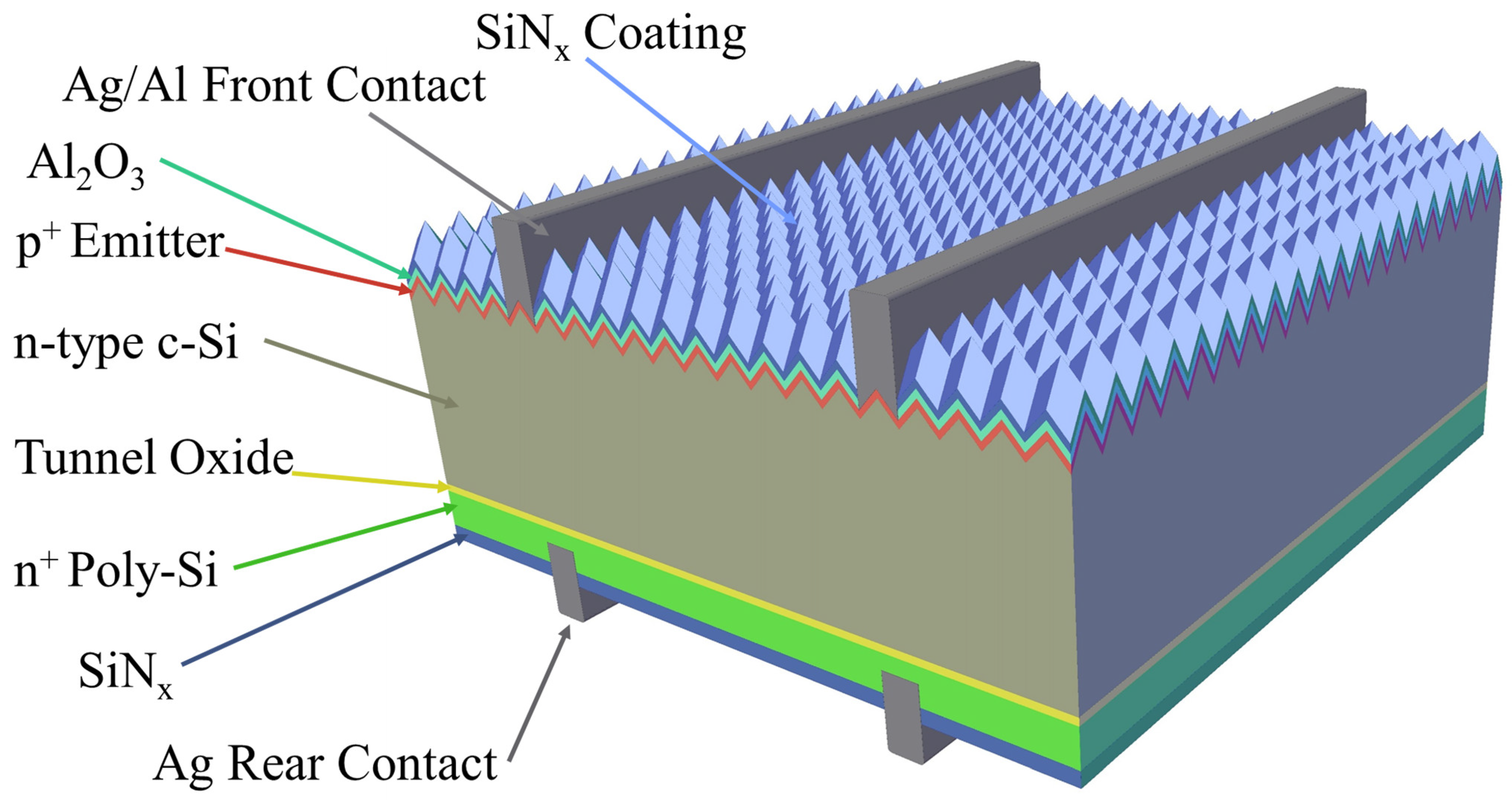
Figure 1. Schematic representation of the tunneling oxide passivated contact (TOPCon) solar cell layout and elemental fabrication.
4. Carrier Transportation Mechanisms at the Poly-Si/SiOx/c-Si Interfaces in the TOPCon Structure
The trends of pinhole and tunneling are two unique forms of charge carrier transportation configurations that arise at interfaces of poly-Si/SiOx/c-Si. Figure 2 demonstrates the situation of carrier transport that happens at the layer of SiOx. Such structures take place according to the width of SiOx thickness and annealing temperatures.
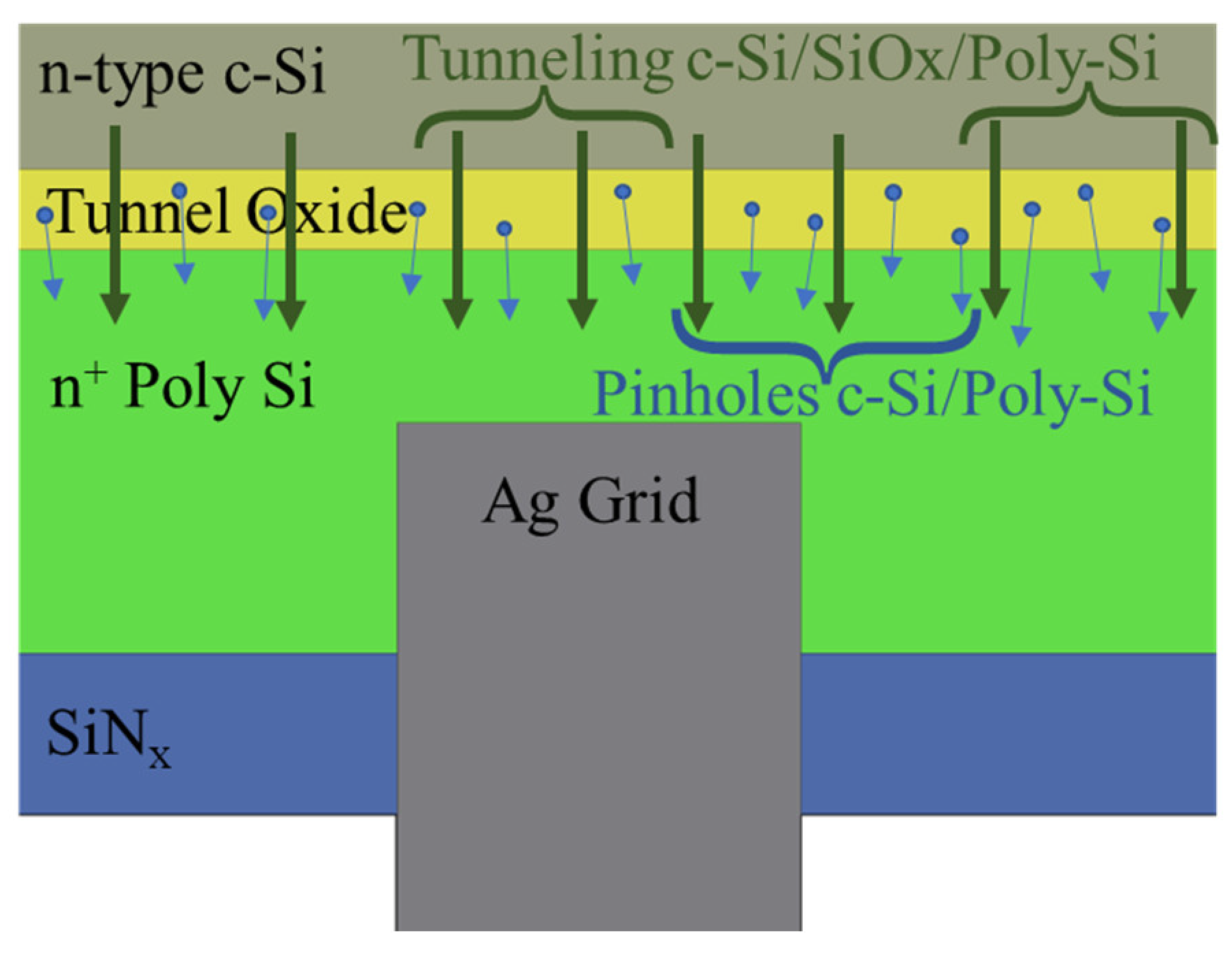
Figure 2. Carrier transportation appearance and formal illustration of tunneling and pinholes phenomenon of the tunnel oxide layer in TOPCon solar cell.
Feldmann et al. explored SiOx tunneling layer experiences maintaining thicknesses of not more than 1.5 nm [13]. The main charge carrier conduction was investigated through the tunneling layer by SiOx. Recent research was enhanced by the simulation modeling performed by Steinkemper et al.
Likewise, the process of the pinhole occurs with a thickness of more than 2 nm of SiOx that is significantly annealed at higher temperatures of approximately 1000 to 1050 °C. The resulting prevalent technique for such kinds of contacts remained precisely controlled over pinholes within the c-Si layer along with poly-Si which were developed through annealing at a high temperature in the SiOx layer [14][15]. Although the oxide layer thickness is conflicting in different progress methods [16], the trend of tunneling takes place in oxides from not more than 2 nm because it is incredibly challenging to tunnel the charge carriers by concentrated oxide coatings [17]. The findings after the performance simulation by Zhang et al. upon nano-scaled tunnel oxide (SiOx, less than 1.5 nm) layer show very high features of tunneling and efficiency by preventing the carrier transport by pinhole [18]. However, a relatively dense SiOx layer (more than 1.1 nm) exhibited minimum fill factor (FF), and efficiency through larger resistivity does not permit any carrier transportation beyond the pinholes.
The transportation of the minimum carrier over the pinholes improves the FF and minimizes the resistance, consequently enhancing the PCE. Wietler et al. analyzed restrain carrier transport by pinholes through selective etching surface of oxide layer on the junction of the POLO structure [19]. A greater density of pinhole concentration would generate maximum saturation current density and negligible contact resistivity (ρc) of approximately 10 mΩ cm2. The thickness of the SiOx layer entails the electrical characteristics of the TOPCon solar cell. The current investigation by Wang et al. described three distinct oxide layer thicknesses as 1.25, 1.42, and 1.55 nm, which exhibited inconsistency in efficiency and other electrical parameters of TOPCon solar cells [20]. At 1.55 nm oxide layer thickness, good quality and regular surface are obtained after the etching, and it holds a minimum J0 value of approximately 18 fA/cm2, with FF = 81.09% and Voc = 687 mV. However, the nano-scaled oxide layer at the thickness of 1.25 and 1.42 nm shows insufficiencies that are ascribed to the passivation failure at the nano-scaled oxide layer along with the pinhole’s progression. Adjusting the accurate temperature for annealing, this one decreases the development of pinhole concentration [21]. The exceptional productivity preceding technology of the TOPCon solar cell continues to determine the specific thickness of the nano-scaled tunnel oxide layer and efficient pinhole concentration for the enhancement in efficiency. The TOPCon solar cell structure holds the lowest value of saturation current density (J0) for equally p-type and n-type poly-Si around (J0 = 2 to 8 fA/cm2). Previously, the doping of poly-Si through phosphorous had better qualities than the poly-Si with boron-doping [22]. However, through research, it became obvious that the n-TOPCon has a good property for the layer of passivation between c-Si wafers of p-type and n-type, demonstrating an excellent value of Voc in comparison with the p-TOPCon [23].
It is not only tunneling that moves the charge through the pinholes; both the transportation through the pinholes and the tunneling occurs together. For example, excessively thick oxide might provide a high tunneling barrier, although charge transfer through pinholes is possible. However, tunneling is more prevalent in the case of dense nano-scaled oxide. The type of conductivity is the factor that matters most. Due to the band-bending orientation, it was shown that p-Si/SiOx/p+-Si can only transport holes and not electrons, and vice versa.
References
- Chen, D.; Chen, Y.; Wang, Z.; Gong, J.; Liu, C.; Zou, Y.; He, Y.; Wang, Y.; Yuan, L.; Lin, W.; et al. 24.58% total area efficiency of screen-printed, large area industrial silicon solar cells with the tunnel oxide passivated contacts (i-TOPCon) design. Sol. Energy Mater. Sol. Cells 2019, 206, 110258.
- Fırat, M.; Radhakrishnan, H.S.; Payo, M.R.; Choulat, P.; Badran, H.; van der Heide, A.; Govaerts, J.; Duerinckx, F.; Tous, L.; Hajjiah, A.; et al. Large-area bifacial n-TOPCon solar cells with in situ phosphorus-doped LPCVD poly-Si passivating contacts. Sol. Energy Mater. Sol. Cells 2022, 236, 111544.
- Yan, D.; Cuevas, A.; Bullock, J.; Wan, Y.; Samundsett, C. Phosphorus-diffused polysilicon contacts for solar cells. Sol. Energy Mater. Sol. Cells 2015, 142, 75–82.
- Rohatgi, A.; Zimbardi, F.; Rounsaville, B.; Benick, J.; Stradins, P.; Norman, A.; Lee, B.; Upadhyaya, A.; Ok, Y.W.; Tao, Y.; et al. Overcoming the Fundamental Bottlenecks to a New World-Record Silicon Solar Cell; Final Technical Report (No. DOE-GT-6336); Georgia Institute of Technology: Atlanta, GA, USA, 2017.
- Green, M.A.; Dunlop, E.D.; Hohl-Ebinger, J.; Yoshita, M.; Kopidakis, N.; Bothe, K.; Hinken, D.; Rauer, M.; Hao, X. Solar cell efficiency tables (Version 60). Prog. Photovolt. Res. Appl. 2022, 30, 687–701.
- Younis, I.M. Cost Benefit Analysis of Photovoltaic Technology Adoption at Rest and Service Area for Malaysia Highway. Ph.D. Thesis, Universiti Teknologi Malaysia, Johor, Malaysia, 2019.
- Lauinger, T.; Schmidt, J.; Aberle, A.G.; Hezel, R. Record low surface recombination velocities on 1 Ω cm p-silicon using remote plasma silicon nitride passivation. Appl. Phys. Lett. 1996, 68, 1232–1234.
- Grant, N.E.; Markevich, V.P.; Mullins, J.; Peaker, A.R.; Rougieux, F.; Macdonald, D.; Murphy, J.D. Permanent annihilation of thermally activated defects which limit the lifetime of float-zone silicon. Phys. Status Solidi (A) 2016, 213, 2844–2849.
- Steinhauser, B.; Feldmann, F.; Polzin, J.I.; Tutsch, L.; Arya, V.; Grübel, B.; Fischer, A.; Moldovan, A.; Benick, J.; Richter, A.; et al. Large area TOPCon Technology Achieving 23.4% Efficiency. In Proceedings of the 2018 IEEE 7th World Conference on Photovoltaic Energy Conversion (WCPEC) (A Joint Conference of 45th IEEE PVSC, 28th PVSEC & 34th EU PVSEC), Waikoloa, HI, USA, 10–15 June 2018; pp. 1507–1510.
- Lindekugel, S.; Lautenschlager, H.; Ruof, T.; Reber, S. Plasma Hydrogen Passivation for Crystalline Silicon Thin-Films. In Proceedings of the 23rd European Photovoltaic Solar Energy Conference, Valencia, Spain, 1–5 September 2008; pp. 2232–2235.
- Richter, A.; Glunz, S.W.; Werner, F.; Schmidt, J.; Cuevas, A. Improved quantitative description of Auger recombination in crystalline silicon. Phys. Rev. 2012, 86, 165202.
- Feldmann, F.; Fellmeth, T.; Steinhauser, B.; Nagel, H.; Ourinson, D.; Mack, S.; Lohmüller, E.; Polzin, J.I.; Benick, J.; Richter, A.; et al. Large Area TOPCon Cells Realized by a PECVD Tube Process. In Proceedings of the 36th European Photovoltaic Solar Energy Conference and Exhibition, Lisbon, Portugal, 10 September 2021.
- Feldmann, F.; Nogay, G.; Loper, P.; Young, D.L.; Lee, B.G.; Stradins, P.; Hermle, M.; Glunz, S.W. Charge carrier transport mechanisms of passivating contacts studied by temperature-dependent JV measurements. Sol. Energy Mater. Sol. Cells 2018, 178, 15–19.
- Haase, F.; Kiefer, F.; Schafer, S.; Kruse, C.; Krugener, J.; Brendel, R.; Peibst, R. Interdigitated back contact solar cells with polycrystalline silicon on oxide passivating contacts for both polarities. Jpn. J. Appl. Phys. 2017, 56, 08MB15.
- Folchert, N.; Rienacker, M.; Yeo, A.A.; Min, B.; Peibst, R.; Brendel, R. Temperature-dependent contact resistance of carrier selective Poly-Si on oxide junctions. Sol. Energy Mater. Sol. Cells 2018, 185, 425–430.
- Richter, A.; Benick, J.; Feldmann, F.; Fell, A.; Steinhauser, B.; Polzin, J.I.; Tucher, N.; Murthy, J.N.; Hermle, M.; Glunz, S.W. September. Both sides contacted silicon solar cells: Options for approaching 26% efficiency. In Proceedings of the 36th European PV Solar Energy Conference and Exhibition, Marseille, France, 9–13 September 2019; pp. 9–13.
- Peibst, R.; Romer, U.; Larionova, Y.; Rienacker, M.; Merkle, A.; Folchert, N.; Reiter, S.; Turcu, M.; Min, B.; Krugener, J.; et al. Working principle of carrier selective poly-Si/c-Si junctions: Is tunnelling the whole story? Sol. Energy Mater. Sol. Cells 2016, 158, 60–67.
- Zhang, Z.; Zeng, Y.; Jiang, C.S.; Huang, Y.; Liao, M.; Tong, H.; Al-Jassim, M.; Gao, P.; Shou, C.; Zhou, X.; et al. Carrier transport through the ultrathin silicon-oxide layer in tunnel oxide passivated contact (TOPCon) c-Si solar cells. Sol. Energy Mater. Sol. Cells 2018, 187, 113–122.
- Wietler, T.F.; Tetzlaff, D.; Krugener, J.; Rienacker, M.; Haase, F.; Larionova, Y.; Brendel, R.; Peibst, R. Pinhole density and contact resistivity of carrier selective junctions with polycrystalline silicon on oxide. Appl. Phys. Lett. 2017, 110, 253902.
- Wang, Q.; Wu, W.; Yuan, N.; Li, Y.; Zhang, Y.; Ding, J. Influence of SiOx film thickness on electrical performance and efficiency of TOPCon solar cells. Sol. Energy Mater. Sol. Cells 2020, 208, 110423.
- Zeng, Y.; Tong, H.; Quan, C.; Cai, L.; Yang, Z.; Chen, K.; Yuan, Z.; Wu, C.H.; Yan, B.; Gao, P.; et al. Theoretical exploration towards high-efficiency tunnel oxide passivated carrier-selective contacts (TOPCon) solar cells. Sol. Energy 2017, 155, 654–660.
- Lenes, M.; Naber, R.C.G.; Luchies, J.R.M. LPCVD Polysilicon Passivated Contacts for Different Solar Cell Concepts. In Proceedings of the 6th Silicon PV Conference, Chambery, France, 7 March 2016.
- Rehman, A.U.; Lee, S.H. Advancements in n-type base crystalline silicon solar cells and their emergence in the photovoltaic industry. Sci. World J. 2013, 2013, 470347.
More
Information
Subjects:
Engineering, Electrical & Electronic
Contributors
MDPI registered users' name will be linked to their SciProfiles pages. To register with us, please refer to https://encyclopedia.pub/register
:
View Times:
4.9K
Revisions:
3 times
(View History)
Update Date:
21 Sep 2022
Table of Contents


Notice
You are not a member of the advisory board for this topic. If you want to update advisory board member profile, please contact office@encyclopedia.pub.
OK
Confirm
Only members of the Encyclopedia advisory board for this topic are allowed to note entries. Would you like to become an advisory board member of the Encyclopedia?
Yes
No
${ textCharacter }/${ maxCharacter }
Submit
Cancel
Back
Comments
${ item }
|
${ item.createdUser.fullName }
${ item.createdAt }
${ item.vote }
${ item.reply }
Delete
${ reply.createdUser.fullName }
${ reply.createdAt }
${ reply.vote }
Delete
There is no reply to this comment~
${ item.replyTextCharacter }/${ item.replyMaxCharacter }
Submit
Cancel
More
No more~
There is no comment~
${ textCharacter }/${ maxCharacter }
Submit
Cancel
${ selectedItem.replyTextCharacter }/${ selectedItem.replyMaxCharacter }
Submit
Cancel
Confirm
Are you sure to Delete?
Yes
No