Your browser does not fully support modern features. Please upgrade for a smoother experience.
Submitted Successfully!
 +1 credit
Thank you for your contribution! You can also upload a video entry or images related to this topic.
For video creation, please contact our Academic Video Service.
| Version | Summary | Created by | Modification | Content Size | Created at | Operation |
|---|---|---|---|---|---|---|
| 1 | Ntalane Sello Seroka | -- | 1975 | 2022-08-15 09:40:59 | | | |
| 2 | Conner Chen | -20 word(s) | 1955 | 2022-08-16 09:06:54 | | | | |
| 3 | Mohammad Raja Ismail AL-SOEIDAT | + 30 word(s) | 1985 | 2025-09-19 12:28:36 | | |
Video Upload Options
We provide professional Academic Video Service to translate complex research into visually appealing presentations. Would you like to try it?
Cite
If you have any further questions, please contact Encyclopedia Editorial Office.
Seroka, N.S.; Taziwa, R.; Khotseng, L.; Al-Soeidat, M.R.I. Solar Cell. Encyclopedia. Available online: https://encyclopedia.pub/entry/26143 (accessed on 23 July 2026).
Seroka NS, Taziwa R, Khotseng L, Al-Soeidat MRI. Solar Cell. Encyclopedia. Available at: https://encyclopedia.pub/entry/26143. Accessed July 23, 2026.
Seroka, Ntalane S., Raymond Taziwa, Lindiwe Khotseng, Mohammad Raja Ismail Al-Soeidat. "Solar Cell" Encyclopedia, https://encyclopedia.pub/entry/26143 (accessed July 23, 2026).
Seroka, N.S., Taziwa, R., Khotseng, L., & Al-Soeidat, M.R.I. (2022, August 15). Solar Cell. In Encyclopedia. https://encyclopedia.pub/entry/26143
Seroka, Ntalane S., et al. "Solar Cell." Encyclopedia. Web. 15 August, 2022.
Copy Citation
The sun is considered a source of clean, renewable energy, and the most abundant. With silicon being the element most used for the direct conversion of solar energy into electrical energy, solar cells are the technology corresponding to the solution of the problem of energy on our planet.
solar cells
semiconductor
thin films
1. Introduction
Their contributions to sustainability and quality of life have led to the desire to develop, manufacture, and find new technologies based on renewable energy resources. Solar energy has proven to be sustainable and has attracted great attention, with the sun considered the most abundant source of clean, renewable energy. This makes solar cell technology economically viable and sustainable and allows for potential reductions in greenhouse gases, thus making it an ideal source of energy while avoiding shortcomings associated with energy and the environment [1][2][3][4]. In addition, solar energy systems are increasingly recognized for their role in achieving global decarbonization targets, supporting energy independence, and creating new economic opportunities in both developed and emerging economies.
Photovoltaics have the ability to generate electrical energy at a lower cost and they are eco-friendly. Thin film solar cells are favorable candidates in the field of photovoltaics because of their minimum material usage and rising efficiencies. The three most commonly known thin film technologies that are extensively studied and still under intensive investigation include α-silicon (α-Si), copper indium gallium selenide (CIGS), and star absorber materials, such as cadmium telluride (CdTe). The conventional inorganic silicon modules, interchangeably known as first generation solar cells, are the leading solar technology for the majority of residential and industrial markets. Presently, crystalline silicon wafers based on a high quality float zone have realized a competitive advantage over traditional solar cells via the utilization of the carrier-selective layer approach [5].
The amorphous silicon incorporated into an intrinsic hydrogen layer placed on one or two sides of the float zone silicon wafer serves as a passivation layer for pre-induced carrier-selective contact. Moreover, the aforementioned architecture recorded a power conversion efficiency of 26.6%, derived from the matrix of interdigitated back contact and heterojunction technologies, approaching the theoretical limit power conversion efficiency (PCE) of 29.1% for a silicon solar cell. In spite of its interesting characteristics and strong scalability for industrial and commercial use, the fabrication costs of this technology have halted, thereby making solar panels costly [5].
Thus, these drawbacks and limitations have led to the desire to research alternative materials such as (CIGS) and (CdTe), identified as second generation thin film photovoltaics, to adequately compensate for the inability of silicon photovoltaics to provide feasible manufacturing and production and generate inexpensive energy. Although crystalline silicon solar cells currently possess greater than 55% of the market share, the module efficiencies of CIGS and CdTe technologies almost rival that of crystalline solar cells, with recorded efficiencies of 21.4% and 21.6%, respectively [5][6][7][8].
Parallel with the emerging materials utilized in thin film technology, most focus is on perovskite solar technology and organic solar cells, as well as dye-sensitized solar cells (DSSCs). These plastic single-junction-based devices exhibit efficiencies of 25.5% [9], 16–18.1% [9][10][11][12][13] and 13% [9][14], respectively. These are third generation solar cells also known as plastic solar cells. Similarly, exfoliated tungsten telluride (WTe) flake (CiGSe) based multilayer thin films have been reported with a PCE of 10.87%. Furthermore, the structural manipulations of the active materials for these cells have garnered immense momentum due to their ease of production, flexibility, and simple fabrication methodologies [14][15].
Several studies have reported on these low-cost, complexity-free, and easily manufactured organic solar cells, more especially the π–conjugated polymers. The comprehensive scientific contribution towards the area of application-specific properties of π–conjugated polymers (viz., design, modelling, and fabrication) in the quest to match the electrical conducting properties exhibited by chemically doped polyacetylene is noteworthy. The aforementioned optoelectronic properties have opened technological interest in various applications, such as nano-electronics, sensors, internet of things (IOT), energy storage photodetectors, memory devices, field effect transistors (FETs), nonlinear optical devices, electrochromic, light emitting diodes (LEDs), and photovoltaics [15][16][17][18][19][20].
The conjugated polymers have interesting features owing to the side-chains present in the polymeric materials, which result in significant thermal stability and solubility, and ultimately promote the fabrication of these nanostructure-based materials by deposition with simple techniques, such as spin coating—hence, their inexpensive and simple solution processability. Their single- and double-bond characteristics and their interesting and adequate π-excessive nature have opened a window of opportunity for newly classified advanced materials in the arena of photonics and electronics [20][21].
The following contents propose to utilize novel polycrystalline silicon semiconductor thin film raw material extracted from sugarcane bagasse ash (SCBA) for solar applications. Currently SCBA is being used as the source of fuel in power-generation boilers to produce electricity. Recent studies have shown that SCBA is rich with mineral content including silicon, iron, and other minerals. The silicon is found mainly in the form of silicic acid and constitutes about 380 kg/ha of silicon composition. It is worth noting that pure silicon is further obtained from silica (SiO2) and it has been reported that the silica is biocompatible and eco-friendly [22][23].
The disposal of bagasse ash waste, therefore, poses a dumping challenge to the environment. Currently, there is very little published information available on the production of silicon nanoparticles from sugarcane bagasse ash for solar applications. Furthermore, quartz is at present the main source of nano silicon. It is obtained by sand mining, which has detrimental effects on the environment such as land degradation, erosion, fissures, and adverse effects on water supply and quality. Metallurgical-grade silicon (MG-Si) (600,000 tons/year) is produced through high-temperature carbothermal reduction of quartz, which requires an energy input of 50 kWh/kg [23][24].
2. Overview of Solar Cell
2.1. Solar Cell Principle of Operation
Solar cells are mainly described based on their architecture; some consist mostly of metals (inorganic thin films), some nanomaterials (QD), some polymers (referred to as organic), etc. Traditionally, solar cells are electronic devices focused on converting sunlight into direct electrical energy as a consequence of the photoelectric effect from metals and inorganic semiconductors [25]. Figure 1 below shows a typical p-n junction silicon solar cell. The generation of electricity comes from the photons (light particles) when sunlight energy shines on the cell. Electrons (−) are ejected from doped Si (n-type) and move across to the positive (+) doped Si (p-type) material as illustrated in Figure 1 below.
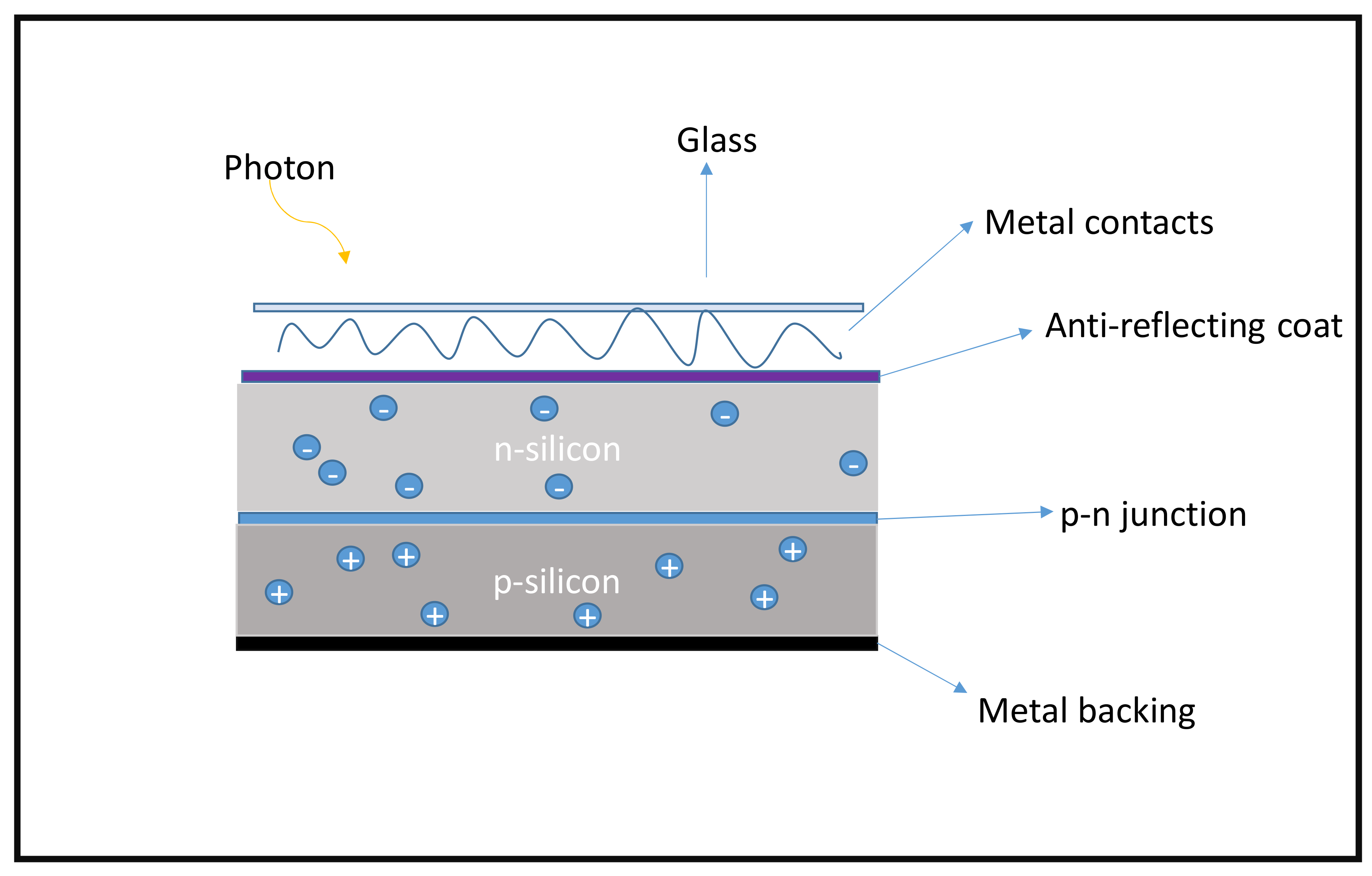
Figure 1. Schematic structure of typical a silicon solar cell [25].
2.1.1. Electronic Structure and Doping Mechanisms in Crystalline Silicon
Electronic Structure
For the originality of electrical conductivity and advanced optical properties, namely low band-gaps in inorganics, it is critical to assimilate the reactivity of these materials, whose electronic configuration is exhibited by doping agents in comparison with undoped inorganic materials. It is well known that the electronic structure of silicon is [Ne] 3s2 3p2, whereby valence electrons avail themselves to form four-bonds with neighboring (adjacent) atoms [26].
Doping Mechanisms of Silicon Materials
The tailoring of materials is performed to attain electrical properties and semiconductor characteristics via doping. This process involves the introduction of foreign materials and/impurities into the bare material, known as the intrinsic semiconductor, to successfully modulate its optical, electrical, and structural properties, ultimately labelled as the extrinsic semiconductor material. As a result of doping, chemical changes are induced within the silicon material, resulting in the generation of charges which migrate within the silicon matrix.
There are various ways and routes to carry out doping including redox, in situ, chemical (gaseous and solution), induced-radiation doping, and charge injection. Additionally, these can be further distinguished by the type of electron transfer, such as doping via reducing agent (n-type) or oxidizing agent (p-type) [26][27][28].
1. P-type Doping
Traditionally, silicon semiconductor doping involves the introduction of foreign materials such as boron and phosphorus to the silicon matrix. The foreign molecules and atoms are referred to as p- and n-type dopants, respectively, due to their electronic nature. Parallel to the concept of an inorganic semiconductor, charge creation emerges from the valence shell during the p-type doping process, as silicon is 1 e- more and thus creates positive charges interchangeably referred to as holes, leaving the whole matrix with a positive charge. This process utilizes oxidizing agents such as boron [5][28].
2. N-type Doping
This process involves the generation of electrons via reducing agents such as phosphorus. In this case, referred to as n-type doping, the silicon matrix is altered as the reducing agent donates electrons, as illustrated in Figure 2, and the matrix generates a negative charge on the surface. N-type doping requires materials with an extra electron compared with the parent structure, silicon, as opposed to their counterpart p-type doping [28][29].
2.2. Important Parameters in a Solar Device
Principle of Charge Separation within a Solar Device
The concept of heterojunction cells relies on the efficient dissociation of an exciton, and the donor and acceptor material’s proximity factor plays a crucial role. The material thickness facilitates the optimum exciton diffusion length, usually a few tenths of a nanometer. Typically, the thickness of the active layer for organic semiconductors is in the range 80–200 nm. Recently, bulk heterojunctions have been deposited via co-sublimation of small molecules and/or the spin coating technique, using mixtures of polymers [30].
The shortcomings faced in heterojunction structures derive from the fact that hole and electron transportation to the electrodes is required in order to promote the separation of charge carriers in order to reach their corresponding electrodes (cathode and anode). For instance, if the individual layer and a given bilayer structure are larger than that of the exciton diffusion length, it is most likely the excitons will recombine as shown in Figure 3, and result in the loss photon indicated by the exciton with the star. Although if the excitons generated are in close proximity to the interface, there is likelihood that they can be separated into free charge carriers and thus diffuse or drift towards their corresponding electrodes, as shown in Figure 2 [30][31][32].
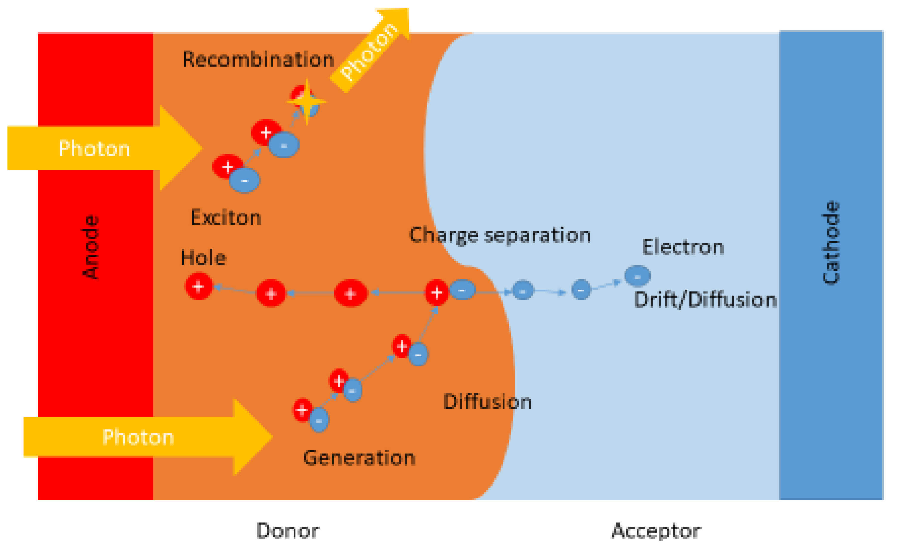
Figure 2. Illustrate the principle of charge separation within a solar cell [30].
It is imperative to know the solar cell performance, as shown in Figure 3, which can be carried out by determining various factors including the fill factor, efficiency, short-circuit current density, and open-circuit voltage [33]. As a result of irradiation, the open-circuit voltage (VOC) is cross-examined as the difference in the cell’s potential at the terminals when there is zero current flow through the terminals. Interestingly, the short-circuit current density (Jsc) is produced from the cell upon irradiation at zero potential.
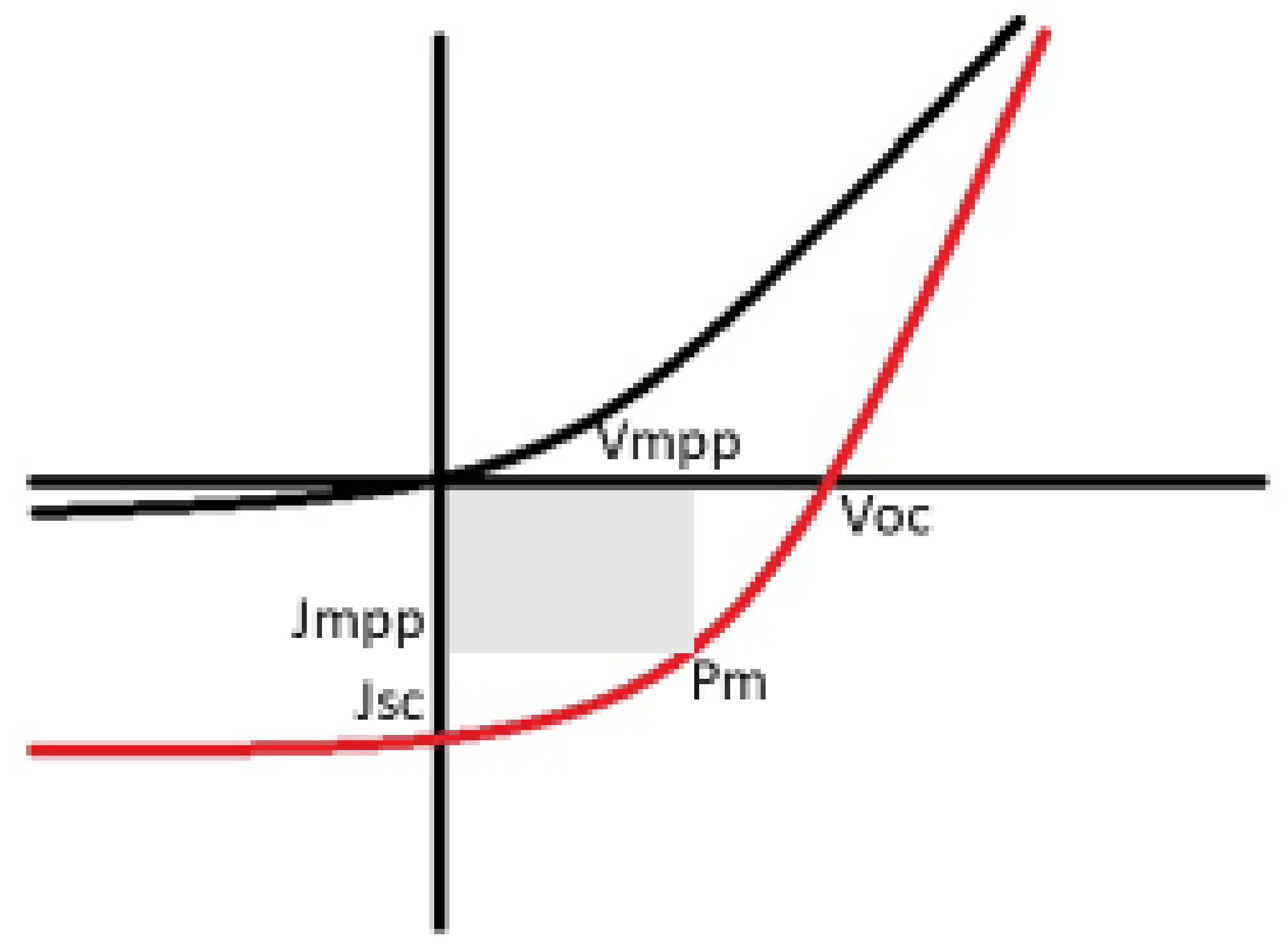
In addition, the fill factor (FF) is known to be the ratio between the cell’s maximum power, shown in Equation (1) where Vmpp and Jmpp denote voltage at the maximum power point and current at the maximum power point, respectively.
Ultimately the power conversion efficiency (PCE) is determined to be the ratio of the cell’s overall output power to incident radiant power.
Innovative designs have made radical developments over the years, whereby thin film solar cell technology results in alternate material device structures. The rising efficiencies of thin film solar cells, in particular perovskite with 23% of the market share, have received significant attention in the photovoltaic market, mostly in the integrated photovoltaic (BIV) field. Plastic solar cells (perovskite) have been rising in efficiency for over two decades, giving them potential as thin film PVs [36].
Thin film solar cells are favorable candidates in the field of photovoltaics because of their minimum material usage and rising efficiencies. The three most commonly known thin film technologies extensively studied and still under intensive investigations include α-silicon (α-Si), copper indium gallium selenide (CIGS), and star absorber materials such as cadmium telluride (CdTe). Photovoltaics have the ability to generate electrical energy at a lower cost and they are environmentally friendly. In spite of the aforementioned property (the power conversion from these devices with an enormous amount of the sun’s energy), these photovoltaic devices still produce about 30% or less of electricity from approximately 80–90% of the sun’s energy absorbed [36][37].
References
- Qazi, A.; Hussain, F.; Rahim, N.A.; Hardaker, G.; Alghazzawi, D.; Shaban, K.; Haruna, K. Towards sustainable energy: A systematic review of renewable energy sources, technologies, and public opinions. IEEE Access 2019, 7, 63837–63851.
- Kumar, M. Social, economic, and environmental impacts of renewable energy resources. In Wind Solar Hybrid Renewable Energy System; Intech Open: London, UK, 2020; Volume 1.
- Ortiz de Zárate, D.; García-Meca, C.; Pinilla-Cienfuegos, E.; Ayúcar, J.A.; Griol, A.; Bellières, L.; Hontañón, E.; Kruis, F.E.; Martí, J. Green and sustainable manufacture of ultrapure engineered nanomaterials. Nanomaterials 2020, 10, 466.
- Miranda, J.; Ponce, P.; Molina, A.; Wright, P. Sensing, smart and sustainable technologies for Agri-Food 4.0. Comput. Ind. 2019, 108, 21–36.
- Bullock, J.; Hettick, M.; Geissbühler, J.; Ong, A.J.; Allen, T.; Sutter-Fella, C.M.; Chen, T.; Ota, H.; Schaler, E.W.; De Wolf, S.; et al. Efficient silicon solar cells with dopant-free asymmetric heterocontacts. Nat. Energy 2016, 1, 1–7.
- Valizadeh, M.; ALRubeei, I.R.N.; ALRikabi, H.T.S.; Abed, F.T. Enhancing the efficiency of photovoltaic power system by submerging it in the rivers. Telkomnika 2022, 20, 166–172.
- Shiyani, T.; Bagchi, T. Hybrid nanostructures for solar-energy-conversion applications. Nanomater. Energy 2020, 9, 39–46.
- Levi, D.H.; Green, M.A.; Hishikawa, Y.; Dunlop, E.D.; Hohl-Ebinger, J.; Ho-Baillie, A.W. Solar cell efficiency tables (version 51). Prog. Photovolt. 2017, 26.
- Rohatgi, A.; Zhu, K.; Tong, J.; Kim, D.H.; Reichmanis, E.; Rounsaville, B.; Prakash, V.; Ok, Y.W. 26.7% Efficient 4-Terminal Perovskite–Silicon Tandem Solar Cell Composed of a High-Performance Semitransparent Perovskite Cell and a Doped Poly-Si/SiOx Passivating Contact Silicon Cell. IEEE J. Photovolt. 2020, 10, 417–422.
- Cui, Y.; Yao, H.; Hong, L.; Zhang, T.; Tang, Y.; Lin, B.; Xian, K.; Gao, B.; An, C.; Bi, P.; et al. Organic photovoltaic cell with 17% efficiency and superior processability. Natl. Sci. Rev. 2020, 7, 1239–1246.
- Yan, T.; Song, W.; Huang, J.; Peng, R.; Huang, L.; Ge, Z. 16.67% rigid and 14.06% flexible organic solar cells enabled by ternary heterojunction strategy. Adv. Mater. 2019, 31, 1902210.
- Cui, Y.; Yao, H.; Zhang, J.; Zhang, T.; Wang, Y.; Hong, L.; Xian, K.; Xu, B.; Zhang, S.; Peng, J.; et al. Over 16% efficiency organic photovoltaic cells enabled by a chlorinated acceptor with increased open-circuit voltages. Nat. Commun. 2019, 10, 1–8.
- Fan, B.; Zhang, D.; Li, M.; Zhong, W.; Zeng, Z.; Ying, L.; Huang, F.; Cao, Y. Achieving over 16% efficiency for single-junction organic solar cells. Sci. China Chem. 2019, 62, 746–752.
- Nair, S.; Patel, S.B.; Gohel, J.V. Recent trends in efficiency-stability improvement in perovskite solar cells. Mater. Today Energy 2020, 17, 100449.
- Kim, D.; Kim, K.M.; Han, H.; Lee, J.; Ko, D.; Park, K.R.; Jang, K.B.; Kim, D.; Forrester, J.S.; Lee, S.H.; et al. Ti/TiO2/SiO2 multilayer thin films with enhanced spectral selectivity for optical narrow bandpass filters. Sci. Rep. 2022, 12, 1–10.
- Terao, J. Synthesis of conjugated polyrotaxanes and its application to molecular wires. In Molecular Architectonics; Springer: Cham, Switzerland, 2017; pp. 487–512.
- Ostroverkhova, O. Organic optoelectronic materials: Mechanisms and applications. Chem. Rev. 2016, 116, 13279–13412.
- Liu, M.; Gao, Y.; Zhang, Y.; Liu, Z.; Zhao, L. Quinoxaline-based conjugated polymers for polymer solar cells. Polym. Chem. 2017, 8, 4613–4636.
- Murad, A.R.; Iraqi, A.; Aziz, S.B.; Abdullah, S.N.; Brza, M.A. Conducting polymers for optoelectronic devices and organic solar cells: A review. Polymers 2020, 12, 2627.
- Moliton, A.; Hiorns, R.C. Review of electronic and optical properties of semiconducting π-conjugated polymers: Applications in optoelectronics. Polym. Int. 2004, 53, 1397–1412.
- Andreão, P.V.; Suleiman, A.R.; Cordeiro, G.C.; Nehdi, M.L. Sustainable use of sugarcane bagasse ash in cement-based materials. Green Mater. 2019, 7, 61–70.
- Savant, N.K.; Korndörfer, G.H.; Datnoff, L.E.; Snyder, G.H. Silicon nutrition and sugarcane production: A review. J. Plant Nutr. 1999, 22, 1853–1903.
- Dhanjode, C.; Nag, A. Utilization of landfill waste in brick manufacturing: A review. Mater. Today Proc. 2022; in press.
- Mustakim, S.M.; Das, S.K.; Mishra, J.; Aftab, A.; Alomayri, T.S.; Assaedi, H.S.; Kaze, C.R. Improvement in fresh, mechanical and microstructural properties of fly ash-blast furnace slag based geopolymer concrete by addition of nano and micro silica. Silicon 2021, 13, 2415–2428.
- Reddy, P.J. Science and Technology of Photovoltaics, 2nd ed.; CRC Press: Leiden, The Netherlands, 2010.
- Guo, Y.; Otley, M.T.; Li, M.; Zhang, X.; Sinha, S.K.; Treich, G.M.; Sotzing, G.A. PEDOT: PSS “wires” printed on textile for wearable electronics. ACS Appl. Mater. Interfaces 2016, 8, 26998–27005.
- Freitag, M.; Teuscher, J.; Saygili, Y.; Zhang, X.; Giordano, F.; Liska, P.; Hua, J.; Zakeeruddin, S.M.; Moser, J.E.; Grätzel, M.; et al. Dye-sensitized solar cells for efficient power generation under ambient lighting. Nat. Photonics 2017, 11, 372–378.
- Krishna, J.V.; Mrinalini, M.; Prasanthkumar, S.; Giribabu, L. Recent advances on porphyrin dyes for dye-sensitized solar cells. Dye.-Sensitized Sol. Cells 2019, 231–284.
- Kietzke, T. Recent advances in organic solar cells. Adv. OptoElectronics 2007, 2007, 1–15.
- Fukuda, K.; Yu, K.; Someya, T. The future of flexible organic solar cells. Adv. Energy Mater. 2020, 10, 2000765.
- Riede, M.; Spoltore, D.; Leo, K. Organic solar cells—the path to commercial success. Adv. Energy Mater. 2021, 11, 2002653.
- Schopp, N.; Brus, V.V.; Lee, J.; Bazan, G.C.; Nguyen, T.Q. A Simple Approach for Unraveling Optoelectronic Processes in Organic Solar Cells under Short-Circuit Conditions. Adv. Energy Mater. 2021, 11, 2002760.
- Abdulrazzaq, O.A.; Saini, V.; Bourdo, S.; Dervishi, E.; Biris, A.S. Organic solar cells: A review of materials, limitations, and possibilities for improvement. Part. Sci. Technol. 2013, 31, 427–442.
- Calado, P.; Telford, A.M.; Bryant, D.; Li, X.; Nelson, J.; O’Regan, B.C.; Barnes, P.R. Evidence for ion migration in hybrid perovskite solar cells with minimal hysteresis. Nat. Commun. 2016, 7, 1–10.
- Sundaram, S.; Shanks, K.; Upadhyaya, H. Thin Film Photovoltaics. In A Comprehensive Guide to Solar Energy Systems; Academic Press: Cambridge, MA, USA, 2018; pp. 361–370.
- Shah, A.; Torres, P.; Tscharner, R.; Wyrsch, N.; Keppner, H. Photovoltaic technology: The case for thin-film solar cells. Science 1999, 285, 692–698.
- Lundberg, O.; Bodegård, M.; Malmström, J.; Stolt, L. Influence of the Cu (In, Ga) Se2 thickness and Ga grading on solar cell performance. Prog. Photovolt. Res. Appl. 2003, 11, 77–88.
More
Information
Subjects:
Chemistry, Physical
Contributors
MDPI registered users' name will be linked to their SciProfiles pages. To register with us, please refer to https://encyclopedia.pub/register
:
View Times:
1.6K
Revisions:
3 times
(View History)
Update Date:
19 Sep 2025
Table of Contents


Notice
You are not a member of the advisory board for this topic. If you want to update advisory board member profile, please contact office@encyclopedia.pub.
OK
Confirm
Only members of the Encyclopedia advisory board for this topic are allowed to note entries. Would you like to become an advisory board member of the Encyclopedia?
Yes
No
${ textCharacter }/${ maxCharacter }
Submit
Cancel
Back
Comments
${ item }
|
${ item.createdUser.fullName }
${ item.createdAt }
${ item.vote }
${ item.reply }
Delete
${ reply.createdUser.fullName }
${ reply.createdAt }
${ reply.vote }
Delete
There is no reply to this comment~
${ item.replyTextCharacter }/${ item.replyMaxCharacter }
Submit
Cancel
More
No more~
There is no comment~
${ textCharacter }/${ maxCharacter }
Submit
Cancel
${ selectedItem.replyTextCharacter }/${ selectedItem.replyMaxCharacter }
Submit
Cancel
Confirm
Are you sure to Delete?
Yes
No