Your browser does not fully support modern features. Please upgrade for a smoother experience.
Submitted Successfully!
 +1 credit
Thank you for your contribution! You can also upload a video entry or images related to this topic.
For video creation, please contact our Academic Video Service.
| Version | Summary | Created by | Modification | Content Size | Created at | Operation |
|---|---|---|---|---|---|---|
| 1 | Kirill A Lozovoy | -- | 2299 | 2022-07-04 13:29:41 | | | |
| 2 | Peter Tang | Meta information modification | 2299 | 2022-07-05 02:21:34 | | |
Video Upload Options
We provide professional Academic Video Service to translate complex research into visually appealing presentations. Would you like to try it?
Cite
If you have any further questions, please contact Encyclopedia Editorial Office.
Lozovoy, K.A.; Izhnin, I.I.; Kokhanenko, A.P.; Dirko, V.V.; Vinarskiy, V.P.; Voitsekhovskii, A.V.; Fitsych, O.I.; Akimenko, N.Y. Single-Element 2D Materials beyond Graphene. Encyclopedia. Available online: https://encyclopedia.pub/entry/24793 (accessed on 23 July 2026).
Lozovoy KA, Izhnin II, Kokhanenko AP, Dirko VV, Vinarskiy VP, Voitsekhovskii AV, et al. Single-Element 2D Materials beyond Graphene. Encyclopedia. Available at: https://encyclopedia.pub/entry/24793. Accessed July 23, 2026.
Lozovoy, Kirill A., Ihor I. Izhnin, Andrey P. Kokhanenko, Vladimir V. Dirko, Vladimir P. Vinarskiy, Alexander V. Voitsekhovskii, Olena I. Fitsych, Nataliya Yu. Akimenko. "Single-Element 2D Materials beyond Graphene" Encyclopedia, https://encyclopedia.pub/entry/24793 (accessed July 23, 2026).
Lozovoy, K.A., Izhnin, I.I., Kokhanenko, A.P., Dirko, V.V., Vinarskiy, V.P., Voitsekhovskii, A.V., Fitsych, O.I., & Akimenko, N.Y. (2022, July 04). Single-Element 2D Materials beyond Graphene. In Encyclopedia. https://encyclopedia.pub/entry/24793
Lozovoy, Kirill A., et al. "Single-Element 2D Materials beyond Graphene." Encyclopedia. Web. 04 July, 2022.
Copy Citation
Thanks to their remarkable mechanical, thermal, electrical, magnetic, and optical properties, 2D materials promise to revolutionize electronics. The unique properties of graphene-like 2D materials give them the potential to create completely new types of devices for functional electronics, nanophotonics, and quantum technologies.
2D materials
two-dimensional allotropes
graphene analogs
molecular beam epitaxy
borophene
aluminene
gallenene
indiene
thallene
silicene
germanene
stanene
plumbene
phosphorene
antimonene
bismuthene
selenene
tellurene
1. Background
Today, two-dimensional materials are one of the key research topics for scientists around the world [1][2][3][4][5]. Since 2004, when the first representative of a new class of materials, a monolayer of carbon atoms, was experimentally obtained in the work by Geim and Novoselov [6], the researchers have seen a real boom in publications on this topic. Over the years, there has been a quantitative and qualitative leap both in the study of graphene itself and of other two-dimensional allotropes—transgraphenes, or X-enes (Figure 1a). As a characteristic numerical indicator confirming the above, the researchers can cite data on the growth in the number of publications that include the keyword “2D material” in the international information and analytical systems of scientific citation Scopus and Web of Science (Figure 1b). By 2022, the number of publications crossed a milestone—more than 10,000 publications on the topic of 2D materials per year (30 articles per day or 1 article every hour).
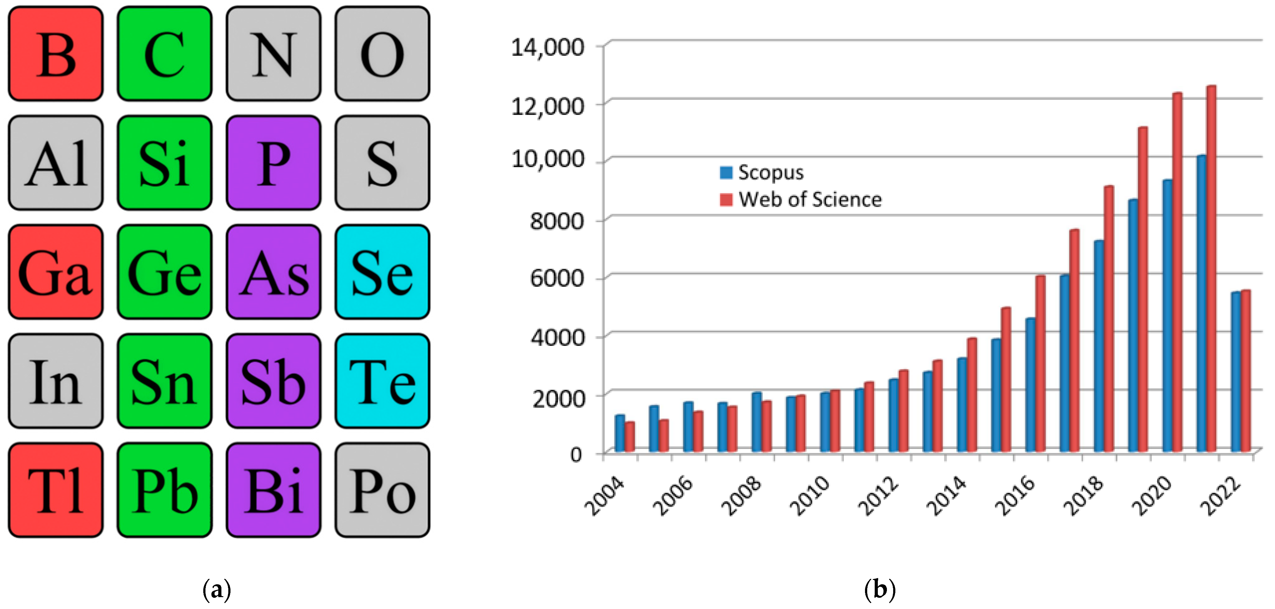
Figure 1. Single-element 2D materials (a) and number of publications with the keyword “2D material” in scientific analytical databases Scopus and Web of Science (b). In the excerption from the periodic table, synthesized single-element two-dimensional materials are highlighted: group IIIA—red, group IVA—green, group VA—violet, group VIA—blue.
This interest in two-dimensional materials is not surprising, since, thanks to their remarkable mechanical, thermal, electrical, magnetic, and optical properties, they promise to revolutionize electronics. Among the outstanding characteristics of 2D materials, the following can be distinguished: very high mobility of charge carriers, extreme strength of graphene due to strong carbon–carbon bonds, the ability to control energy structure and bandgap by changing the material composition, and a simple defect structure due only to the presence of vacancies and impurities. In addition, under certain conditions, exotic quantum effects can manifest in these materials: they can be topological insulators and high-temperature superconductors. The unique properties of 2D materials make them promising for the creation of completely new types of devices for functional electronics, nanophotonics, and quantum technologies [7][8][9][10][11][12].
Nowadays, the following existing two-dimensional allotropic modifications can be distinguished: graphene (C) and its analogs (transgraphenes or X-enes) borophene (B), aluminene (Al), gallenene (Ga), indiene (In), thallene (Tl), silicene (Si), germanene (Ge), stanene (Sn), plumbene (Pb), phosphorene (P), arsenene (As), antimonene (Sb), bismuthene (Bi), selenene (Se), and tellurene (Te) (Figure 1a).
They are very closely related to graphene and transgraphene derivatives functionalized by hydrogen ions (graphane (CH)n, silicane (SiH)n, germanane (GeH)n, and other transgraphanes (or X-anes) with the general formula (GH)n, where G is one of the elements that form the initial two-dimensional material: C, Si, Sn, Pb, B, P, etc.) or other ligands (for example, metal cations, hydroxyl groups, organic radicals, with the general formula (GR)n) [13].
2. Structural Characteristics of Single-Element 2D Materials
The concept of a two-dimensional allotropic modification of silicon was proposed in 1994 [14]. Subsequently, the new material was actively studied by theorists and was named “silicene” by analogy with graphene [15]. All graphene-like materials of elements of group IVA are characterized by mixed sp2–sp3 hybridization [16]. Unlike graphene (Figure 2a), the lattice of silicene, germanene, stanene, and plumbene is not absolutely flat, but curved. Their structure can be represented as two sublattices displaced relative to each other in the vertical direction (Figure 2b). Such curved honeycomb structure and ordered buckling of the surface lead to exceptional stability and increased flexibility compared with graphene. This geometry defines the wide spectrum of their potential applications in electronics [17][18][19]. Such a buckled hexagonal structure was also observed in all further works on the synthesis of transgraphenes of group IVA [20][21][22][23][24][25][26][27][28][29][30][31][32][33][34][35][36][37][38][39][40][41][42][43][44][45][46][47][48][49][50][51][52][53][54][55][56][57][58].

Figure 2. Honeycomb lattice of graphene (a) and graphene-like structure of two-dimensional materials of group IVA (b) (on this and following figures colored balls represent atoms and black lines represent interatomic bonds).
The data on the lattice parameters of group IVA graphene-like 2D materials (silicene, germanene, stanene, and plumbene) such as the distance l between nearest atoms in the honeycomb structure, the lattice constant a, and the displacement parameter between the upper and lower atoms δ are reviewed in Table 1.
Table 1. Structural parameters of the buckled honeycomb lattice of graphene and group IVA transgraphenes.
|
Material |
Distance l between Atoms |
Lattice Constant a |
Buckling Parameter δ |
References |
|---|---|---|---|---|
|
nm |
nm |
nm |
||
|
Graphene |
0.14 |
0.25 |
0 |
|
|
Silicene |
0.23 |
0.39 |
0.08 |
|
|
Germanene |
0.25 |
0.40 |
0.09 |
|
|
Stanene |
0.28 |
0.47 |
0.10 |
|
|
Plumbene |
0.30 |
0.49 |
0.10 |
Borophene, aluminene, gallenene, indiene, and thallene—representatives of group IIIA transgraphenes—can have various modifications of the crystal lattice [59][60][61][62][63][64][65][66][67][68][69][70][71][72][73].
Borophene has a flat or curved structure, consisting of many equilateral triangles, forming a two-dimensional network (Figure 3). In this case, its structure can be considered as a solid solution of the composition B1−vVv, where v is the concentration of vacancies V of boron atoms. When there are no vacancies of boron atoms, borophene has a curved lattice with the parameter δ ≈ 0.08 nm (Figure 3a), and in the presence of vacancies with the concentration v = 1/6, its structure becomes flat (Figure 3b). Borophene structures with a different v are also possible. The distance between boron atoms in the borophene structure is about 0.17 nm [2][59].
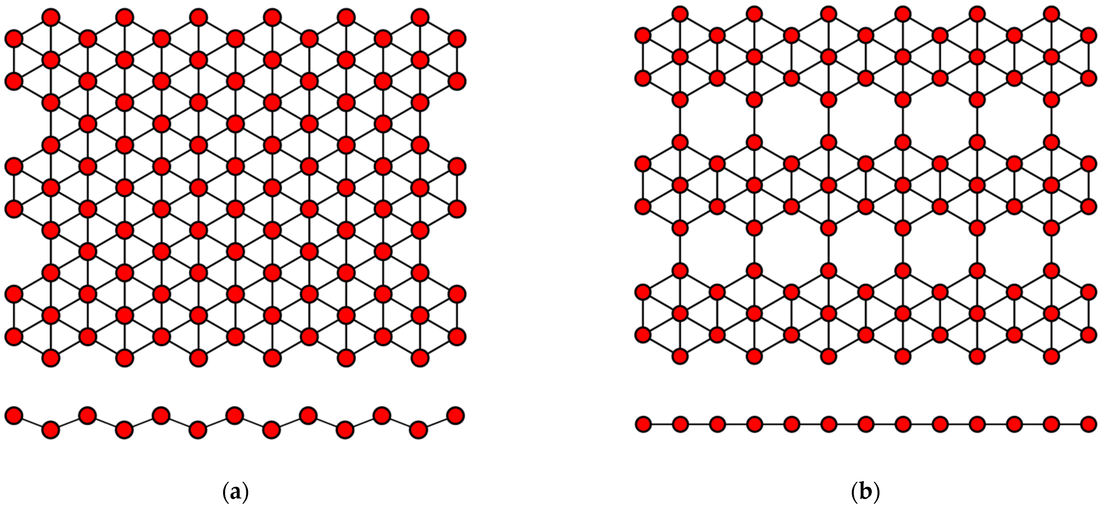
Figure 3. Variants of the structure of the crystal lattice of borophene for (a) v = 0 and (b) v = 1/6.
Gallenene has a flat honeycomb structure similar to graphene (Figure 2a), or a slightly curved configuration such as group IVA transgraphenes (Figure 2b). The crystal lattice parameters of gallenene have the following values: the distance between the gallium atoms is l = 0.25 nm, the lattice constant a is about 0.39 nm, and the buckling parameter δ = 0–0.08 nm [63][64].
Aluminene has not yet been synthesized experimentally, but theoretical calculations using the density functional theory predict the possibility of its existence with a crystal lattice such as graphene, borophene, or even phosphorene (Figure 4). Thus, aluminene can have a flat, buckled, or puckered structure [67][68]. For the graphene-like modification of the aluminene crystal lattice, the distance between aluminum atoms is predicted to be l ≈ 0.26 nm [65].

Figure 4. Two variants of the crystal structure of phosphorene: (a) puckered (α-phase) and (b) buckled (β-phase).
The two-dimensional allotropic modification of indium (indiene) is also predicted only theoretically so far. Presumably, it can have three variants of the crystal structure: flat (like in graphene) (Figure 2a), buckled (like in transgraphenes of group IVA) (Figure 2b), or puckered (like in phosphorene) (Figure 4a). For all modifications of indiene, the calculated distance between indium atoms is l ≈ 0.29 nm, and the lattice constant is a ≈ 0.5 nm for the flat geometry and a ≈ 0.425 nm for the buckled one at δ ≈ 0.15 nm [65][70][71][72].
The last representative of group IIIA transgraphenes, thallene, was synthesized in 2020 on the NiSi2/Si(111) surface [73] in the form of a flat honeycomb structure similar to graphene (Figure 2a), with parameter l ≈ 0.38 nm. Density functional theory calculations predict for a free-standing thallene l = 0.3 nm (Table 2).
Table 2. Parameters of the honeycomb lattice of group IIIA transgraphenes (materials predicted only theoretically and not obtained experimentally are marked with * sign).
The first representative of transgraphenes of group VA, phosphorene can be in two modifications: puckered (or α-phase) (Figure 4a) and buckled (or β-phase) (Figure 4b). The lattice parameters of phosphorene have the following values: the distance between phosphorus atoms is l = 0.23 nm, the lattice constant a is about 0.33 nm, and the buckling parameter δ = 0.12 nm [72][74].
For the two-dimensional modification of arsenic (arsenene), theoretical calculations predict the following lattice parameters: the distance between arsenic atoms is l = 0.25 nm, the lattice constant a is about 0.36 nm, and the buckling parameter δ = 0.14 nm [75][76].
Experimental studies of the synthesis of two-dimensional antimony (antimonene) turned out to be quite successful, and today this material has already been fabricated on a large number of substrates [77][78][79][80][81][82]. The distance between antimony atoms ranges from 0.29 nm and more, depending on the substrate; the lattice constant is slightly more than 0.4 nm and δ ≈ 0.17 nm [75][78].
For bismuthene, a two-dimensional allotropic modification of bismuth, the lattice constant of a curved graphene-like structure was calculated to be a = 0.434 nm [72]. However, its actual value may increase depending on the substrate [83] (Table 3).
Table 3. Parameters of the honeycomb lattice of group VA transgraphenes.
Finally, let us take a look at the structural properties of single-element 2D materials from the group VIA. The stable states of the two-dimensional modification of selenium (selenene) were first calculated within the framework of the density functional theory in 2017 [84]. Then, their electrical, thermoelectric, and thermal properties were theoretically investigated [85][86][87][88]. Two modifications of the crystal lattice are predicted for selenene and tellurene (Figure 5).
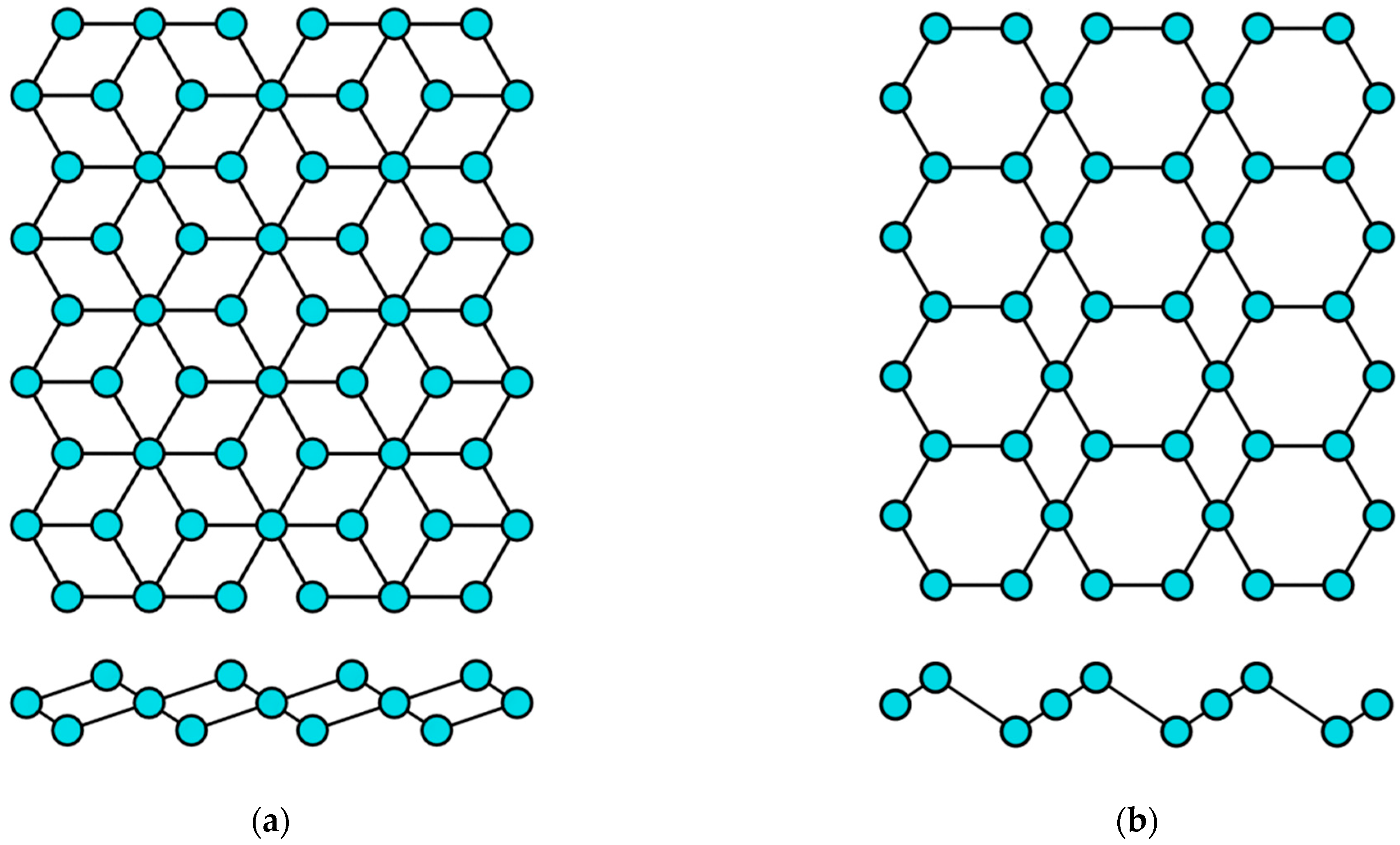
Figure 5. Two variants of the crystal structure of selenene and tellurene: (a) α-phase and (b) β-phase.
According to the theoretical calculations, the distance between atoms in selenene should be l ≈ 0.27 nm [88]. The two-dimensional tellurium layer (tellurene) has the same crystal structure modifications as selenene (Figure 5), and its lattice parameter l is about 0.3 nm [88][89][90] (Table 4).
Table 4. Parameters of the honeycomb lattice of group VIA transgraphenes.
Thus, numerous experimental studies confirmed the curved structure of transgraphenes and also showed that such a structure is more flexible than that of graphene, which makes it possible to control the energy spectra by adjusting the synthesis conditions.
3. Epitaxial Fabrication of Single-Element 2D Materials
3.1. Group IIIA Single-Element 2D Materials
Borophene, the first representative of 2D materials of group IIIA, was first synthesized experimentally on Ag(111) substrate in 2015 [59][60]. Earlier attempts at heteroepitaxial fabrication of borophene were complicated by a low barrier of the formation of three-dimensional boron islands [91]. Therefore, it was necessary to carefully select a suitable substrate in order to overcome this unwanted 3D island formation. A low threshold for nucleation of two-dimensional clusters was found on a number of metal substrates, which facilitated the formation of extended layers of large-area single-crystal borophene. Among them are Al(111) [92], Au(111) [93], Cu(111) [94], and Ir(111) [95] (Figure 6). In this case the nearest-neighbor distance of the potential substrate for the fabrication of 2D material should match with the lattice parameter a of the honeycomb lattice. In addition to metal substrates, the possibility of obtaining layers of two-dimensional boron modification on surfaces such as transition metal diborides [96][97] with the (0001) orientation is predicted.

Figure 6. Model of borophene layer on a metal substrate.
3.2. Group IVA Single-Element 2D Materials
Unlike graphene, a monolayer of carbon atoms with sp2-hybridization, which can be fabricated by simple exfoliation of single layers from graphite due to weak interlayer interaction, atom-thick layers of silicon, germanium, tin, or lead are not so readily exfoliated from the corresponding bulk materials because they have sp3-hybridization with strong covalent bonds. Consequently, the current task is to find methods of synthesis of transgraphenes other than exfoliation technique. Moreover, one of the basic methods of fabrication of silicene, germanene, stanene, and plumbene today is the heteroepitaxy on the surfaces matched by the lattice parameter [24].
For the first time, silicene was experimentally obtained by epitaxial methods in 2012 on Ag (111) substrate [20][21]. In this work, Ag(111) plates were cleaned by Ar+ sputtering with the energy 1.5 keV. Then, the substrates were annealed at the 500–600 °C to obtain atomically smooth silver surface. Silicon was deposited with the rate of 0.01–0.03 ML/min on the silver surface heated to 200–300 °C [20][21]. Later on, research on the growth of silicene on Ag(111) surface at various temperatures was carried out, and the important role of the substrate temperature in the formation of transgraphene structures was established [25]. It was shown that the number of defects in a honeycomb lattice increases with temperature, and silicene does not form at the temperatures of 330 °C or higher.
After that, silicene was synthesized on Ir(111) [24], Pb(111) [48], ZrB2(0001) [26], MoS2 [27], ZrC [28], Ru [29], and graphite [30] surfaces. For some substrates, to obtain uniform monolayer with honeycomb lattice, post-growth annealing of the synthesized structures was implemented. As in the previous case of single-element 2D materials of group IIIA, to serve a perfect surface for the group IVA buckled allotropes formation, the substrate should have lattice constant close to that of the desired 2D material, so that three of six atoms in the honeycomb mesh coincide with the nearest three atoms of the substrate (Figure 7).
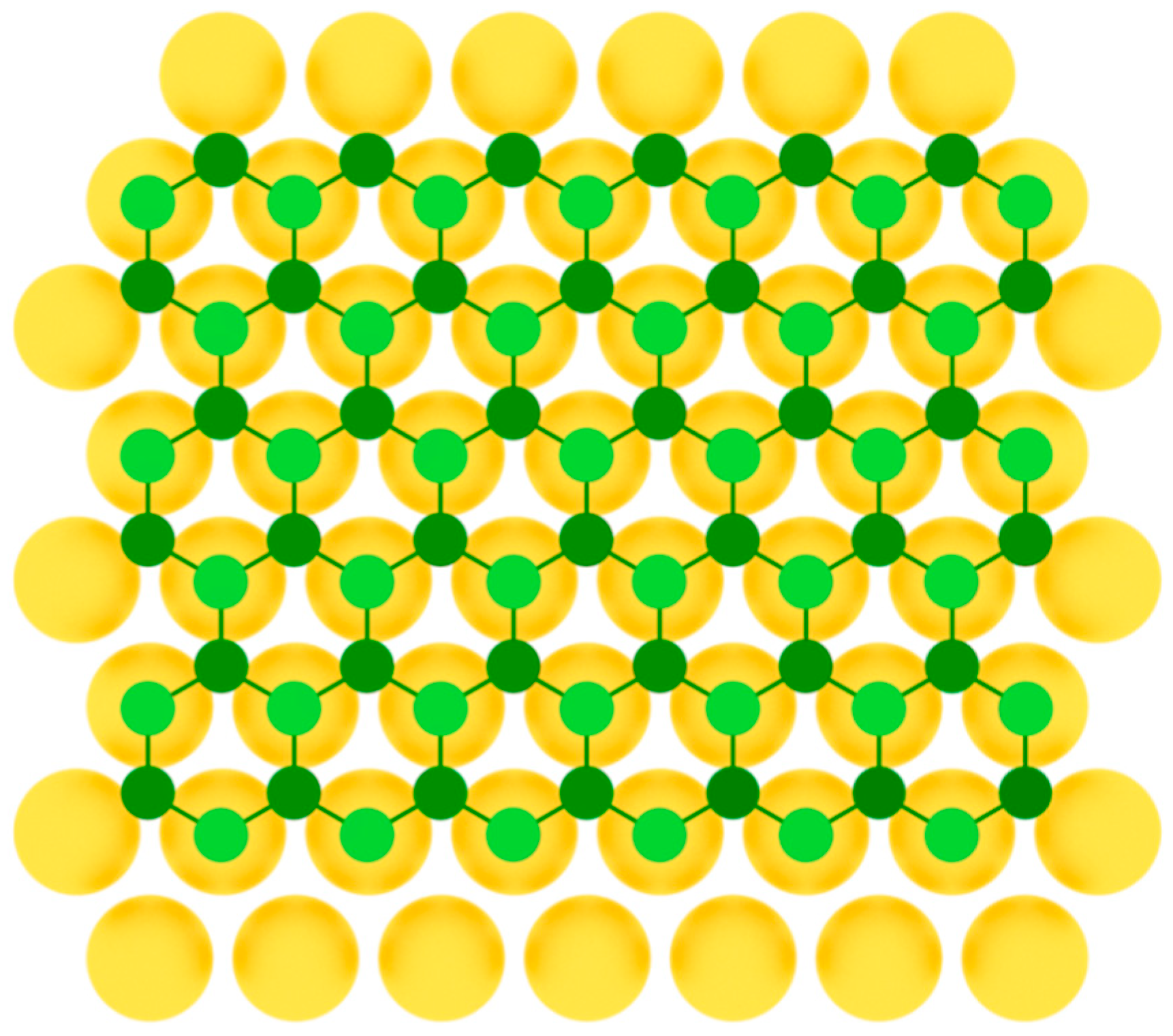
Figure 7. Model of buckled silicene layer on a metal substrate (two colors are used for silicon atoms at different height positions).
3.3. Group VA Single-Element 2D Materials
Phosphorene was first produced by an exfoliation technique [98] and later fabricated in the method of molecular beam epitaxy on Au(111) substrate [99]. In work [99], clean Au(111) substrate was prepared by repeated Ar+ bombardment with ion energy of 1.5 keV at the pressure of about 1·10−5 Torr and subsequent annealing at 500 °C. Phosphorus was deposited by evaporation from a crucible containing bulk black phosphorus at 260 °C. During the deposition process, the substrate temperature was below 260 °C, so the initial growth stage involved the condensation of P4 molecules from the gas phase onto Au(111) surface. Then, the system was annealed at 250 °C for 60 min until well-defined monolayer phosphorus with a hexagonal structure appeared [99]. This was achieved due to the close lattice parameters of phosphorene and the substrate (Figure 8).

Figure 8. Model of phosphorene layer on a metal substrate (two colors are used for phosphorus atoms at different height positions).
3.4. Group VIA Single-Element 2D Materials
To date, selenene was synthesized only by physical vapor deposition on Si(111) substrate in the work [100].
Tellurene was first obtained on flexible mica substrates by van der Waals epitaxy in 2014 in [101]. Thereafter, tellurium was successfully grown heteroepitaxially on highly oriented pyrolytic graphite [89] and graphene [102] (Figure 9).
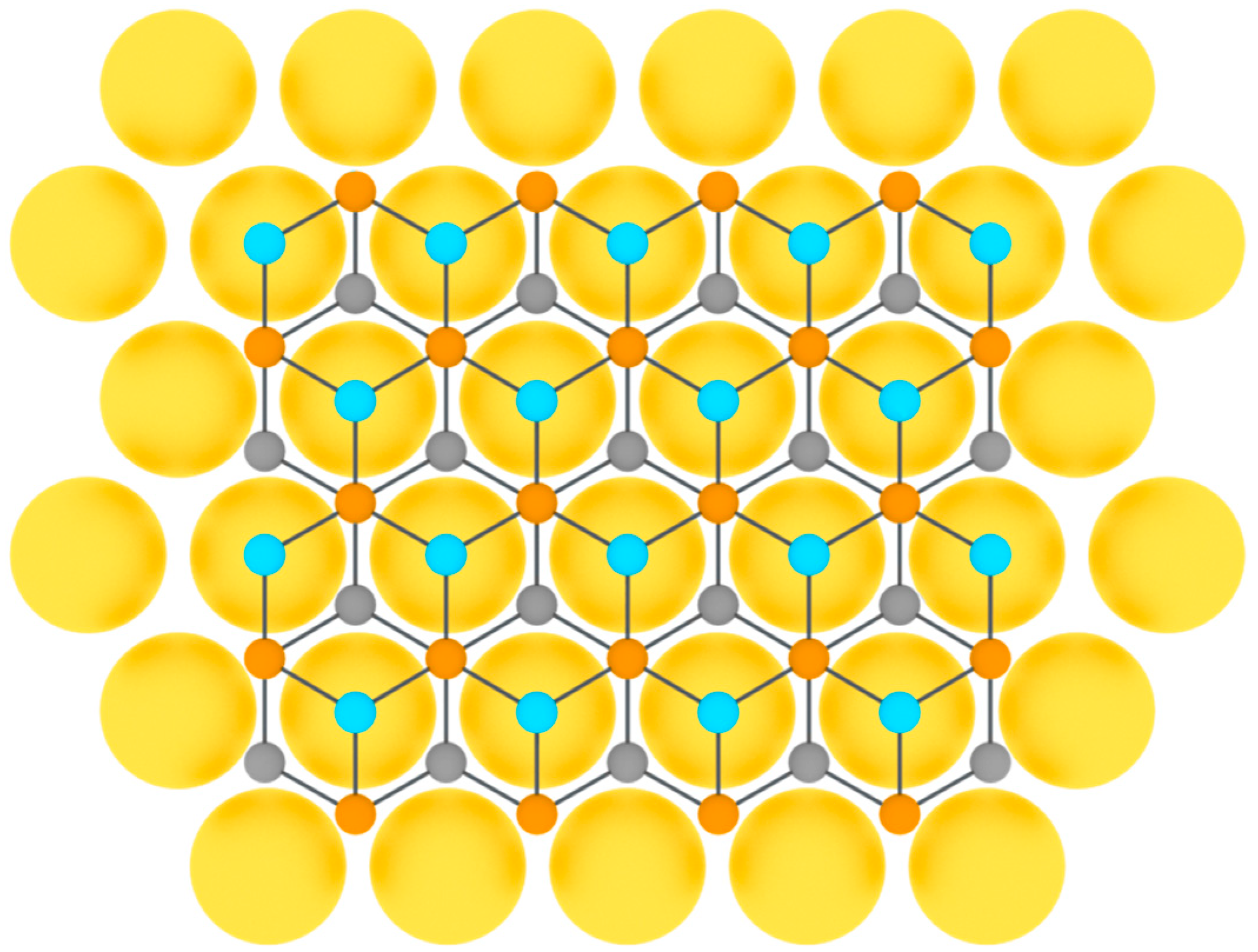
Figure 9. Model of tellurene layer on a substrate (three colors are used for tellurium atoms at different height positions).
References
- Khan, K.; Tareen, A.K.; Iqbal, M.; Wang, L.; Ma, C.; Shi, Z.; Ye, Z.; Ahmad, W.; Sagar, R.U.R.; Shams, S.S.; et al. Navigating recent advances in monoelemental materials (Xenes)-fundamental to biomedical applications. Prog. Solid State Chem. 2021, 63, 100326.
- Zhou, D.; Li, H.; Si, N.; Li, H.; Fuchs, H.; Niu, T. Epitaxial Growth of Main Group Monoelemental 2D Materials. Adv. Funct. Mater. 2020, 31.
- Ponomarenko, V.P.; Popov, V.S.; Popov, S.V.; Chepurnov, E.L. Photo- and Nanoelectronics Based on Two-Dimensional Materials. Part I. Two-Dimensional Materials: Properties and Synthesis. J. Commun. Technol. Electron. 2020, 65, 1062–1104.
- Li, X.; Tao, L.; Chen, Z.; Fang, H.; Li, X.; Wang, X.; Xu, J.-B.; Zhu, H. Graphene and related two-dimensional materials: Structure-property relationships for electronics and optoelectronics. Appl. Phys. Rev. 2017, 4, 021306.
- Molle, A.; Goldberger, J.; Houssa, M.; Xu, Y.; Zhang, S.-C.; Akinwande, D. Buckled two-dimensional Xene sheets. Nat. Mater. 2017, 16, 163–169.
- Novoselov, K.S.; Geim, A.K.; Morozov, S.V.; Jiang, D.; Zhang, Y.; Dubonos, S.V.; Grigorieva, I.V.; Firsov, A.A. Electric field effect in atomically thin carbon films. Science 2004, 306, 666–669.
- Acun, A.; Zhang, L.; Bampoulis, P.; Farmanbar, M.; Van Houselt, A.; Rudenko, A.N.; Lingenfelder, M.; Brocks, G.; Poelsema, B.; I Katsnelson, M.; et al. Germanene: The germanium analogue of graphene. J. Phys. Condens. Matter 2015, 27, 443002.
- Tao, L.; Cinquanta, E.; Chiappe, D.; Grazianetti, C.; Fanciulli, M.; Dubey, M.; Molle, A.; Akinwande, D. Silicene field-effect transistors operating at room temperature. Nat. Nanotechnol. 2015, 10, 227–231.
- Houssa, M.; van den Broek, B.; Iordanidou, K.; Lu, A.K.A.; Pourtois, G.; Locquet, J.P.; Afanas’ev, V.; Stesmans, A. Topological to trivial insulating phase transition in stanene. Nano Res. 2016, 9, 774–778.
- Mortazavi, B.; Dianat, A.; Cuniberti, G.; Rabczuk, T. Application of silicene, germanene and stanene for Na or Li ion storage: A theoretical investigation. Electrochim. Acta 2016, 213, 865–870.
- Garg, P.; Choudhuri, I.; Pathak, B. Stanene based gas sensors: Effect of spin–orbit coupling. Phys. Chem. Chem. Phys. 2017, 19, 31325–31334.
- Liao, M.; Zang, Y.; Guan, Z.; Li, H.; Gong, Y.; Zhu, K.; Hu, X.-P.; Zhang, D.; Xu, Y.; Wang, Y.-Y.; et al. Superconductivity in few-layer stanene. Nat. Phys. 2018, 14, 344–348.
- Lozovoy, K.A.; Dirko, V.V.; Vinarskiy, V.P.; Kokhanenko, A.P.; Voitsekhovskii, A.V.; Akimenko, N.Y. Two-dimensional materials of group IVA: Latest advances in epitaxial methods of growth. Russ. Phys. J. 2022, 64, 1583–1591.
- Takeda, K.; Shiraishi, K. Theoretical possibility of stage corrugation in Si and Ge analogs of graphite. Phys. Rev. B 1994, 50, 14916–14922.
- Guzman-Veri, G.G.; Lew Yan Voon, L.C. Electronic structure of silicon-based nanostructures. Phys. Rev. B. 2007, 76, 075131.
- Molle, A.; Grazianetti, C.; Tao, L.; Taneja, D.; Alam, H.; Akinwande, D. Silicene, silicene derivatives, and their device applications. Chem. Soc. Rev. 2018, 47, 6370–6387.
- Jose, D.; Datta, A. Structures and electronic properties of silicene clusters: A promising material for FET and hydrogen storage. Phys. Chem. Chem. Phys. 2011, 13, 7304–7311.
- Houssa, M.; Dimoulas, A.; Molle, A. Silicene: A review of recent experimental and theoretical investigations. J. Phys. Condens. Matter 2015, 27, 253002.
- Le Lay, G. Silicene transistors. Nat. Nanotechnol. 2015, 10, 202–203.
- Vogt, P.; De Padova, P.; Quaresima, C.; Avila, J.; Frantzeskakis, E.; Asensio, M.C.; Resta, A.; Ealet, B.; Le Lay, G. Silicene: Compelling Experimental Evidence for Graphenelike Two-Dimensional Silicon. Phys. Rev. Lett. 2012, 108, 155501.
- Lin, C.-L.; Arafune, R.; Kawahara, K.; Tsukahara, N.; Minamitani, E.; Kim, Y.; Takagi, N.; Kawai, M. Structure of Silicene Grown on Ag(111). Appl. Phys. Express 2012, 5, 045802.
- Ezawa, M. Monolayer Topological Insulators: Silicene, Germanene, and Stanene. J. Phys. Soc. Jpn. 2015, 84.
- Balendhran, S.; Walia, S.; Nili, H.; Sriram, S.; Bhaskaran, M. Elemental Analogues of Graphene: Silicene, Germanene, Stanene, and Phosphorene. Small 2015, 11, 640–652.
- Meng, L.; Wang, Y.; Zhang, L.; Du, S.; Wu, R.; Li, L.; Zhang, Y.; Li, G.; Zhou, H.; Hofer, W.A.; et al. Buckled Silicene Formation on Ir(111). Nano Lett. 2013, 13, 685–690.
- Jamgotchian, H.; Colignon, Y.; Hamzaoui, N.; Ealet, B.; Hoarau, J.Y.; Aufray, B.; Bibérian, J.P. Growth of silicene layers on Ag(111): Unexpected effect of the substrate temperature. J. Phys. Condens. Matter 2012, 24, 172001.
- Fleurence, A.; Friedlein, R.; Ozaki, T.; Kawai, H.; Wang, Y.; Yamada-Takamura, Y. Experimental Evidence for Epitaxial Silicene on Diboride Thin Films. Phys. Rev. Lett. 2012, 108, 245501.
- Chiappe, D.; Scalise, E.; Cinquanta, E.; Grazianetti, C.; van der Broek, B.; Fanciulli, M.; Houssa, M.; Molle, A. Two-Dimensional Si Nanosheets with Local Hexagonal Structure on a MoS2 Surface. Adv. Mater. 2013, 26, 2096–2101.
- Aizawa, T.; Suehara, S.; Otani, S. Silicene on Zirconium Carbide (111). J. Phys. Chem. C 2014, 118, 23049–23057.
- Huang, L.; Zhang, Y.-F.; Zhang, Y.-Y.; Xu, W.; Que, Y.; Li, E.; Pan, J.-B.; Wang, Y.; Liu, Y.; Du, S.-X.; et al. Sequence of Silicon Monolayer Structures Grown on a Ru Surface: From a Herringbone Structure to Silicene. Nano Lett. 2017, 17, 1161–1166.
- De Crescenzi, M.; Berbezier, I.; Scarselli, M.; Castrucci, P.; Abbarchi, M.; Ronda, A.; Jardali, F.; Park, J.; Vach, H. Formation of Silicene Nanosheets on Graphite. ACS Nano 2016, 10, 11163–11171.
- Jahangirov, S.; Topsakal, M.; Akturk, E.; Sahin, H.; Ciraci, S. Two- and One-Dimensional Honeycomb Structures of Silicon and Germanium. Phys. Rev. Lett. 2009, 102, 236804.
- Derivaz, M.; Dentel, D.; Stephan, R.; Hanf, M.-C.; Mehdaoui, A.; Sonnet, P.; Pirri, C. Continuous Germanene Layer on Al(111). Nano Lett. 2015, 15, 2510–2516.
- Zhang, L.; Bampoulis, P.; Rudenko, A.N.; Yao, Q.; van Houselt, A.; Poelsema, B.; Katsnelson, M.I.; Zandvliet, H.J.W. Structural and electronic properties of germanene on MoS2. Phys. Rev. Lett. 2016, 116, 256804.
- Dávila, M.E.; Le Lay, G. Few layer epitaxial germanene: A novel two-dimensional Dirac material. Sci. Rep. 2016, 6, 20714.
- Dávila, M.E.; Xian, L.; Jahangirov, S.; Rubio, A.; Le Lay, G. Germanene: A novel two-dimensional germanium allotrope akin to graphene and silicene. New J. Phys. 2014, 16.
- Li, L.; Lu, S.-Z.; Pan, J.; Qin, Z.; Wang, Y.-Q.; Wang, Y.; Cao, G.-Y.; Du, S.; Gao, H.-J. Buckled Germanene Formation on Pt(111). Adv. Mater. 2014, 26, 4820–4824.
- d’Acapito, F.; Torrengo, S.; Xenogiannopoulou, E.; Tsipas, P.; Marquez Velasco, J.; Tsoutsou, D.; Dimoulas, A. Evidence for germanene growth on epitaxial hexagonal (h)-AlN on Ag(111). J. Phys. Condens. Matt. 2016, 28, 045002.
- Webb, R. Future stuff: Stanene. New Sci. 2014, 224, 38–39.
- Gross, M. Stanene the next miracle material? Chem. Ind. 2014, 78, 24–27.
- Sahoo, S.K.; Wei, K. A Perspective on Recent Advances in 2D Stanene Nanosheets. Adv. Mater. Interfaces 2019, 6, 1900752.
- Zhu, F.; Chen, W.; Xu, Y.; Gao, C.-L.; Guan, D.-D.; Liu, C.-H.; Qian, D.; Zhang, S.-C.; Jia, J.-F. Epitaxial growth of two-dimensional stanene. Nat. Mater. 2015, 14, 1020–1025.
- Gou, J.; Kong, L.; Li, H.; Zhong, Q.; Li, W.; Cheng, P.; Chen, L.; Wu, K. Strain-induced band engineering in monolayer stanene on Sb(111). Phys. Rev. Mater. 2017, 1, 054004.
- Xu, C.-Z.; Chan, Y.-H.; Chen, P.; Wang, X.; Flötotto, D.; Hlevyack, J.A.; Bian, G.; Mo, S.-K.; Chou, M.-Y.; Chiang, T.-C. Gapped electronic structure of epitaxial stanene on InSb(111). Phys. Rev. B 2018, 97, 035122.
- Yuhara, J.; Fujii, Y.; Nishino, K.; Isobe, N.; Nakatake, M.; Xian, L.; Rubio, A.; Le Lay, G. Large area planar stanene epitaxially grown on Ag(1 1 1). 2D Mater. 2018, 5, 025002.
- Yuhara, J.; He, B.; Matsunami, N.; Nakatake, M.; Le Lay, G. Graphene’s latest cousin: Plumbene epitaxial growth on a “Nano WaterCube”. Adv. Mater. 2019, 31, 1901017.
- Yuhara, J.; Le Lay, G. Beyond silicene: Synthesis of germanene, stanene and plumbene. Jpn. J. Appl. Phys. 2020, 59, SN0801.
- Bihlmayer, G.; Sassmannshausen, J.; Kubetzka, A.; Blügel, S.; von Bergmann, K.; Wiesendanger, R. Plumbene on a Magnetic Substrate: A Combined Scanning Tunneling Microscopy and Density Functional Theory Study. Phys. Rev. Lett. 2020, 124, 126401.
- Stepniak-Dybala, A.; Krawiec, M. Formation of silicene on ultrathin Pb(111) films. J. Phys. Chem. C 2019, 123, 17019–17025.
- Gou, J.; Zhong, Q.; Sheng, S.; Li, W.; Cheng, P.; Li, H.; Chen, L.; Wu, K. Strained monolayer germanene with 1 × 1 lattice on Sb(111). 2D Mater. 2016, 3, 045005.
- Persichetti, L.; Jardali, F.; Vach, H.; Sgarlata, A.; Berbezier, I.; De Crescenzi, M.; Balzarotti, A. van der Waals Heteroepitaxy of Germanene Islands on Graphite. J. Phys. Chem. Lett. 2016, 7, 3246–3251.
- Peng, W.B.; Xu, T.; Diener, P.; Biadala, L.; Berthe, M.; Pi, X.D.; Borensztein, Y.; Curcella, A.; Bernard, R.; Prévot, G.; et al. Resolving the Controversial Existence of Silicene and Germanene Nanosheets Grown on Graphite. ACS Nano 2018, 12, 4754–4760.
- Qin, Z.; Pan, J.; Lu, S.; Shao, Y.; Wang, Y.; Du, S.; Gao, H.-J.; Cao, G. Direct Evidence of Dirac Signature in Bilayer Germanene Islands on Cu(111). Adv. Mater. 2017, 29, 1606046.
- Yao, Q.; Zhang, L.; Kabanov, N.S.; Rudenko, A.N.; Arjmand, T.; Soleimani, H.R.; Klavsyuk, A.L.; Zandvliet, H.J.W. Bandgap opening in hydrogenated germanene. Appl. Phys. Lett. 2018, 112, 171607.
- Van Bremen, R.; Bampoulis, P.; Aprojanz, J.; Smithers, M.; Poelsema, B.; Tegenkamp, C.; Zandvliet, H.J.W. Ge2Pt hut clusters: A substrate for germanene. J. Appl. Phys. 2018, 124, 125301.
- Zhuang, J.; Liu, C.; Zhou, Z.; Casillas, G.; Feng, H.; Xu, X.; Wang, J.; Hao, W.; Wang, X.; Dou, S.X.; et al. Dirac Signature in Germanene on Semiconducting Substrate. Adv. Sci. 2018, 5, 1800207.
- Deng, J.; Xia, B.; Ma, X.; Chen, H.; Shan, H.; Zhai, X.; Li, B.; Zhao, A.; Xu, Y.; Duan, W.; et al. Epitaxial growth of ultraflat stanene with topological band inversion. Nat. Mater. 2018, 17, 1081–1086.
- Chen, K.-C.; Lee, L.-M.; Chen, H.-A.; Sun, H.; Wu, C.-L.; Chen, H.-A.; Lin, K.-B.; Tseng, Y.-C.; Kaun, C.-C.; Pao, C.-W.; et al. Multi-layer elemental 2D materials: Antimonene, germanene and stanene grown directly on molybdenum disulfides. Semicond. Sci. Technol. 2019, 34, 105020.
- Pang, W.; Nishino, K.; Ogikubo, T.; Araidai, M.; Nakatake, M.; Le Lay, G.; Yuhara, J. Epitaxial growth of honeycomb-like stanene on Au(111). Appl. Surf. Sci. 2020, 517, 146224.
- Mannix, A.J.; Zhou, X.-F.; Kiraly, B.; Wood, J.D.; Alducin, D.; Myers, B.D.; Liu, X.; Fisher, B.L.; Santiago, U.; Guest, J.R.; et al. Synthesis of borophenes: Anisotropic, two-dimensional boron polymorphs. Science 2015, 350, 1513–1516.
- Feng, B.; Zhang, J.; Zhong, Q.; Li, W.; Li, S.; Li, H.; Cheng, P.; Meng, S.; Chen, L.; Wu, K. Experimental realization of two-dimensional boron sheets. Nat. Chem. 2016, 8, 563–568.
- Penev, E.S.; Kutana, A.; Yakobson, B.I. Can Two-Dimensional Boron Superconduct? Nano Lett. 2016, 16, 2522–2526.
- Liu, X.; Li, Q.; Ruan, Q.; Rahn, M.S.; Yakobson, B.I.; Hersam, M.C. Borophene synthesis beyond the single-atomic-layer limit. Nat. Mater. 2021, 21, 35–40.
- Kochat, V.; Samanta, A.; Zhang, Y.; Bhowmick, S.; Manimunda, P.; Asif, S.A.S.; Stender, A.S.; Vajtai, R.; Singh, A.K.; Tiwary, C.S.; et al. Atomically thin gallium layers from solid-melt exfoliation. Sci. Adv. 2018, 4, e1701373.
- Tao, M.-L.; Tu, Y.-B.; Sun, K.; Wang, Y.-L.; Xie, Z.-B.; Liu, L.; Shi, M.-X.; Wang, J.-Z. Gallenene epitaxially grown on Si(1 1 1). 2D Mater. 2018, 5, 035009.
- Khalil, B.A.; Gaston, N. Two-dimensional aluminium, gallium, and indium metallic crystals by first-principles design. J. Phys. Condens. Matter. 2021, 33, 125901.
- Kamal, C.; Chakrabarti, A.; Ezawa, M. Aluminene as highly hole-doped graphene. New J. Phys. 2015, 17.
- Yuan, J.-H.; Yu, N.; Xue, K.-H.; Miao, X. Stability, electronic and thermodynamic properties of aluminene from first-principles calculations. Appl. Surf. Sci. 2017, 409, 85–90.
- Yeoh, K.H.; Yoon, T.L.; Rusi; Ong, D.S.; Lim, T.L. First-principles studies on the superconductivity of aluminene. Appl. Surf. Sci. 2018, 445, 161–166.
- Lukačević, I.; Pajtler, M.V.; Mužević, M.; Gupta, S.K. Prospects for experimental realization of two-dimensional aluminium allotropes. J. Mater. Chem. C 2019, 7, 2666–2675.
- Singh, D.; Gupta, S.K.; Lukačević, I.; Sonvane, Y. Indiene 2D monolayer: A new nanoelectronic material. RSC Adv. 2016, 6, 8006–8014.
- Singh, D.; Gupta, S.K.; Lukačević, I.; Mužević, M.; Sonvane, Y.; Ahuja, R. Effect of electric field on optoelectronic properties of indiene monolayer for photoelectric nanodevices. Sci. Rep. 2019, 9, 17300.
- Le, M.-Q.; Nguyen, H.-T.; Bui, T.-L. Fracture of 28 buckled two-dimensional hexagonal sheets. Mech. Adv. Mater. Struct. 2021, 1–13.
- Gruznev, D.V.; Bondarenko, L.V.; Tupchaya, A.Y.; Mihalyuk, A.N.; Eremeev, S.V.; Zotov, A.V.; Saranin, A.A. Thallene: Graphene-like honeycomb lattice of Tl atoms frozen on single-layer NiSi2. 2D Mater. 2020, 7, 045026.
- Zhu, Z.; Tománek, D. Semiconducting Layered Blue Phosphorus: A Computational Study. Phys. Rev. Lett. 2014, 112, 176802.
- Xu, Y.; Peng, B.; Zhang, H.; Shao, H.; Zhang, R.; Zhu, H. First-principle calculations of optical properties of monolayer arsenene and antimonene allotropes. Ann. Phys. 2017, 529, 1600152.
- Beladi-Mousavi, S.M.; Pourrahimi, A.M.; Sofer, Z.; Pumera, M. Atomically Thin 2D-Arsenene by Liquid-Phased Exfoliation: Toward Selective Vapor Sensing. Adv. Funct. Mater. 2018.
- Fortin-Deschênes, M.; Waller, O.; Menteş, T.O.; Locatelli, A.; Mukherjee, S.; Genuzio, F.; Levesque, P.; Hébert, A.; Martel, R.; Moutanabbir, O. Synthesis of Antimonene on Germanium. Nano Lett. 2017, 17, 4970–4975.
- Wu, X.; Shao, Y.; Liu, H.; Feng, Z.; Wang, Y.-L.; Sun, J.-T.; Liu, C.; Wang, J.-O.; Liu, Z.-L.; Zhu, S.-Y.; et al. Epitaxial Growth and Air-Stability of Monolayer Antimonene on PdTe2. Adv. Mater. 2016, 29, 1605407.
- Shao, Y.; Liu, Z.-L.; Cheng, C.; Wu, X.; Liu, H.; Liu, C.; Wang, J.-O.; Zhu, S.-Y.; Wang, Y.-Q.; Shi, D.-X.; et al. Epitaxial Growth of Flat Antimonene Monolayer: A New Honeycomb Analogue of Graphene. Nano Lett. 2018, 18, 2133–2139.
- Jałochowski, M.; Krawiec, M. Antimonene on Pb quantum wells. 2D Mater. 2019, 6, 045028.
- Lei, T.; Li, J.-M.; Li, F.-S.; Wang, J.-O.; Ibrahim, K.; Zhang, K. Anisotropic electronic structure of antimonene. Appl. Phys. Lett. 2019, 115, 221602.
- Niu, T.; Zhou, W.; Zhou, D.; Hu, X.; Zhang, S.; Zhang, K.; Zhou, M.; Fuchs, H.; Zeng, H. Modulating Epitaxial Atomic Structure of Antimonene through Interface Design. Adv. Mater. 2019, 31, e1902606.
- Reis, F.; Li, G.; Dudy, L.; Bauernfeind, M.; Glass, S.; Hanke, W.; Thomale, R.; Schäfer, J.; Claessen, R. Bismuthene on a SiC substrate: A candidate for a high-temperature quantum spin Hall material. Science 2017, 357, 287–290.
- Xian, L.; Paz, A.P.; Bianco, E.; Ajayan, P.M.; Rubio, A. Square selenene and tellurene: Novel group VI elemental 2D materials with nontrivial topological properties. 2D Mater. 2017, 4, 041003.
- Wang, D.; Tang, L.-M.; Jiang, X.-X.; Tan, J.-Y.; He, M.-D.; Wang, X.-J.; Chen, K.-Q. High Bipolar Conductivity and Robust In-Plane Spontaneous Electric Polarization in Selenene. Adv. Electron. Mater. 2018, 5, 1800475.
- Lin, C.; Cheng, W.; Chai, G.; Zhang, H. Thermoelectric properties of two-dimensional selenene and tellurene from group-VI elements. Phys. Chem. Chem. Phys. 2018, 20, 24250–24256.
- Liu, G.; Gao, Z.; Li, G.-L.; Wang, H. Abnormally low thermal conductivity of 2D selenene: An ab initio study. J. Appl. Phys. 2020, 127, 065103.
- Ramírez-Montes, L.; López-Pérez, W.; Gonzalez-Hernandez, R.; Pinilla, C. Large thermoelectric figure of merit in hexagonal phase of 2D selenium and tellurium. Int. J. Quantum Chem. 2020, 120, 26267.
- Chen, J.; Dai, Y.; Ma, Y.; Dai, X.; Ho, W.; Xie, M. Ultrathin β-tellurium layers grown on highly oriented pyrolytic graphite by molecular-beam epitaxy. Nanoscale 2017, 9, 15945–15948.
- Zhu, Z.; Cai, X.; Yi, S.; Chen, J.; Dai, Y.; Niu, C.; Guo, Z.X.; Xie, M.; Liu, F.; Cho, J.-H.; et al. Multivalency-Driven Formation of Te-Based Monolayer Materials: A Combined First-Principles and Experimental study. Phys. Rev. Lett. 2017, 119, 106101.
- Zhang, Z.; Penev, E.S.; Yakobson, B.I. Two-dimensional boron: Structures, properties and applications. Chem. Soc. Rev. 2017, 46, 6746–6763.
- Li, W.; Kong, L.; Chen, C.; Gou, J.; Sheng, S.; Zhang, W.; Li, H.; Chen, L.; Cheng, P.; Wu, K. Experimental realization of honeycomb borophene. Sci. Bull. 2018, 63, 282–286.
- Kiraly, B.; Liu, X.; Wang, L.; Zhang, Z.; Mannix, A.J.; Fisher, B.L.; Yakobson, B.I.; Hersam, M.C.; Guisinger, N.P. Borophene Synthesis on Au(111). ACS Nano 2019, 13, 3816–3822.
- Wu, R.; Drozdov, I.K.; Eltinge, S.; Zahl, P.; Ismail-Beigi, S.; Božović, I.; Gozar, A. Large-area single-crystal sheets of borophene on Cu(111) surfaces. Nat. Nanotechnol. 2019, 14, 44–49.
- Vinogradov, N.A.; Lyalin, A.; Taketsugu, T.; Vinogradov, A.S.; Preobrajenski, A. Single-phase borophene on Ir(111): Formation, structure, and decoupling from the support. ACS Nano. 2019, 13, 14511–14518.
- Suehara, S.; Aizawa, T.; Sasaki, T. Graphenelike surface boron layer: Structural phases on transition-metal diborides (0001). Phys. Rev. B 2010, 81, 085423.
- Qin, N.; Liu, S.; Li, Z.; Zhao, H.; Wang, S. First-principles studies for the stability of a graphene-like boron layer on CrB2(0001) and MoB2(0001). J. Phys. Condens. Matter 2011, 23, 225501.
- Castellanos-Gomez, A.; Vicarelli, L.; Prada, E.; Island, J.O.; Narasimha-Acharya, K.L.; Blanter, S.I.; Groenendijk, D.J.; Buscema, M.; Steele, G.A.; Alvarez, J.V.; et al. Isolation and characterization of few-layer black phosphorus. 2D Mater. 2014, 1, 025001.
- Zhang, J.L.; Zhao, S.; Han, C.; Wang, Z.; Zhong, S.; Sun, S.; Guo, R.; Zhou, X.; Gu, C.D.; Di Yuan, K.; et al. Epitaxial Growth of Single Layer Blue Phosphorus: A New Phase of Two-Dimensional Phosphorus. Nano Lett. 2016, 16, 4903–4908.
- Qin, J.; Qiu, G.; Jian, J.; Zhou, H.; Yang, L.; Charnas, A.; Zemlyanov, D.Y.; Xu, C.-Y.; Xu, X.; Wu, W.; et al. Controlled Growth of a Large-Size 2D Selenium Nanosheet and Its Electronic and Optoelectronic Applications. ACS Nano 2017, 11, 10222–10229.
- Wang, Q.; Safdar, M.; Xu, K.; Mirza, M.; Wang, Z.; He, J. Van der Waals Epitaxy and Photoresponse of Hexagonal Tellurium Nanoplates on Flexible Mica Sheets. ACS Nano 2014, 8, 7497–7505.
- Huang, X.; Guan, J.; Lin, Z.; Liu, B.; Xing, S.; Wang, W.; Guo, J. Epitaxial Growth and Band Structure of Te Film on Graphene. Nano Lett. 2017, 17, 4619–4623.
More
Information
Subjects:
Quantum Science & Technology
Contributors
MDPI registered users' name will be linked to their SciProfiles pages. To register with us, please refer to https://encyclopedia.pub/register
:
View Times:
2.4K
Revisions:
2 times
(View History)
Update Date:
05 Jul 2022
Table of Contents


Notice
You are not a member of the advisory board for this topic. If you want to update advisory board member profile, please contact office@encyclopedia.pub.
OK
Confirm
Only members of the Encyclopedia advisory board for this topic are allowed to note entries. Would you like to become an advisory board member of the Encyclopedia?
Yes
No
${ textCharacter }/${ maxCharacter }
Submit
Cancel
Back
Comments
${ item }
|
${ item.createdUser.fullName }
${ item.createdAt }
${ item.vote }
${ item.reply }
Delete
${ reply.createdUser.fullName }
${ reply.createdAt }
${ reply.vote }
Delete
There is no reply to this comment~
${ item.replyTextCharacter }/${ item.replyMaxCharacter }
Submit
Cancel
More
No more~
There is no comment~
${ textCharacter }/${ maxCharacter }
Submit
Cancel
${ selectedItem.replyTextCharacter }/${ selectedItem.replyMaxCharacter }
Submit
Cancel
Confirm
Are you sure to Delete?
Yes
No