Your browser does not fully support modern features. Please upgrade for a smoother experience.
Please note this is a comparison between Version 1 by Kirill A Lozovoy and Version 2 by Peter Tang.
Thanks to their remarkable mechanical, thermal, electrical, magnetic, and optical properties, 2D materials promise to revolutionize electronics. The unique properties of graphene-like 2D materials give them the potential to create completely new types of devices for functional electronics, nanophotonics, and quantum technologies.
- 2D materials
- two-dimensional allotropes
- graphene analogs
- molecular beam epitaxy
- borophene
- aluminene
- gallenene
- indiene
- thallene
- silicene
- germanene
- stanene
- plumbene
- phosphorene
- antimonene
- bismuthene
- selenene
- tellurene
1. Background
Today, two-dimensional materials are one of the key research topics for scientists around the world [1][2][3][4][5][1,2,3,4,5]. Since 2004, when the first representative of a new class of materials, a monolayer of carbon atoms, was experimentally obtained in the work by Geim and Novoselov [6], the researchers have seen a real boom in publications on this topic. Over the years, there has been a quantitative and qualitative leap both in the study of graphene itself and of other two-dimensional allotropes—transgraphenes, or X-enes (Figure 1a). As a characteristic numerical indicator confirming the above, the researchers can cite data on the growth in the number of publications that include the keyword “2D material” in the international information and analytical systems of scientific citation Scopus and Web of Science (Figure 1b). By 2022, the number of publications crossed a milestone—more than 10,000 publications on the topic of 2D materials per year (30 articles per day or 1 article every hour).
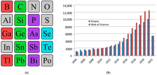
Figure 1. Single-element 2D materials (a) and number of publications with the keyword “2D material” in scientific analytical databases Scopus and Web of Science (b). In the excerption from the periodic table, synthesized single-element two-dimensional materials are highlighted: group IIIA—red, group IVA—green, group VA—violet, group VIA—blue.
This interest in two-dimensional materials is not surprising, since, thanks to their remarkable mechanical, thermal, electrical, magnetic, and optical properties, they promise to revolutionize electronics. Among the outstanding characteristics of 2D materials, the following can be distinguished: very high mobility of charge carriers, extreme strength of graphene due to strong carbon–carbon bonds, the ability to control energy structure and bandgap by changing the material composition, and a simple defect structure due only to the presence of vacancies and impurities. In addition, under certain conditions, exotic quantum effects can manifest in these materials: they can be topological insulators and high-temperature superconductors. The unique properties of 2D materials make them promising for the creation of completely new types of devices for functional electronics, nanophotonics, and quantum technologies [7][8][9][10][11][12][7,8,9,10,11,12].
Nowadays, the following existing two-dimensional allotropic modifications can be distinguished: graphene (C) and its analogs (transgraphenes or X-enes) borophene (B), aluminene (Al), gallenene (Ga), indiene (In), thallene (Tl), silicene (Si), germanene (Ge), stanene (Sn), plumbene (Pb), phosphorene (P), arsenene (As), antimonene (Sb), bismuthene (Bi), selenene (Se), and tellurene (Te) (Figure 1a).
They are very closely related to graphene and transgraphene derivatives functionalized by hydrogen ions (graphane (CH)n, silicane (SiH)n, germanane (GeH)n, and other transgraphanes (or X-anes) with the general formula (GH)n, where G is one of the elements that form the initial two-dimensional material: C, Si, Sn, Pb, B, P, etc.) or other ligands (for example, metal cations, hydroxyl groups, organic radicals, with the general formula (GR)n) [13].
2. Structural Characteristics of Single-Element 2D Materials
The concept of a two-dimensional allotropic modification of silicon was proposed in 1994 [14]. Subsequently, the new material was actively studied by theorists and was named “silicene” by analogy with graphene [15]. All graphene-like materials of elements of group IVA are characterized by mixed sp2–sp3 hybridization [16]. Unlike graphene (Figure 2a), the lattice of silicene, germanene, stanene, and plumbene is not absolutely flat, but curved. Their structure can be represented as two sublattices displaced relative to each other in the vertical direction (Figure 2b). Such curved honeycomb structure and ordered buckling of the surface lead to exceptional stability and increased flexibility compared with graphene. This geometry defines the wide spectrum of their potential applications in electronics [17][18][19][17,18,19]. Such a buckled hexagonal structure was also observed in all further works on the synthesis of transgraphenes of group IVA [20][21][22][23][24][25][26][27][28][29][30][31][32][33][34][35][36][37][38][39][40][41][42][43][44][45][46][47][48][49][50][51][52][53][54][55][56][57][58][20,21,22,23,24,25,26,27,28,29,30,31,32,33,34,35,36,37,38,39,40,41,42,43,44,45,46,47,48,49,50,51,52,53,54,55,56,57,58].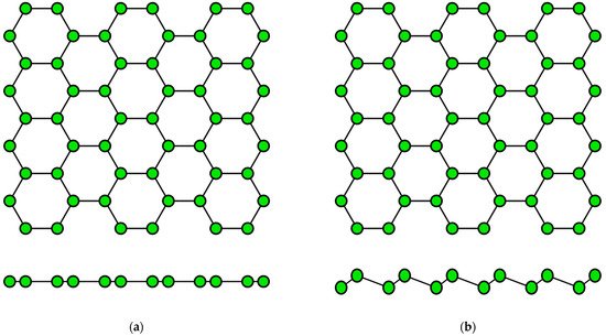
Figure 2. Honeycomb lattice of graphene (a) and graphene-like structure of two-dimensional materials of group IVA (b) (on this and following figures colored balls represent atoms and black lines represent interatomic bonds).
Table 1.
Structural parameters of the buckled honeycomb lattice of graphene and group IVA transgraphenes.
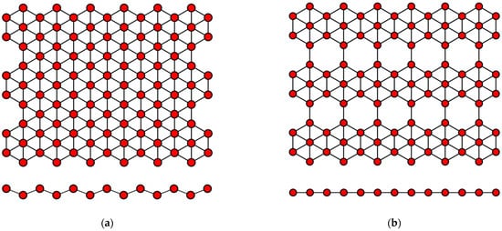
Figure 3.
Variants of the structure of the crystal lattice of borophene for (
a
)
v
= 0 and (
b
)
v
= 1/6.
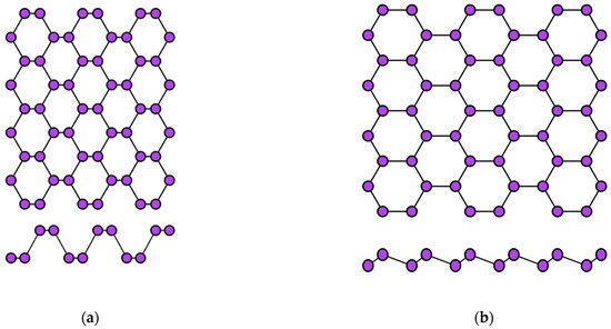
Figure 4.
Two variants of the crystal structure of phosphorene: (
a
) puckered (α-phase) and (
b
) buckled (β-phase).
Table 2.
Parameters of the honeycomb lattice of group IIIA transgraphenes (materials predicted only theoretically and not obtained experimentally are marked with
*
sign).
Table 3.
Parameters of the honeycomb lattice of group VA transgraphenes.
|
Material |
Distance l between Atoms |
Lattice Constant a |
Buckling Parameter δ |
|---|
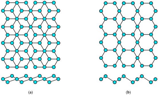
Figure 5.
Two variants of the crystal structure of selenene and tellurene: (
a
) α-phase and (
b
) β-phase.
Table 4.
Parameters of the honeycomb lattice of group VIA transgraphenes.
|
Material |
Distance l between Atoms |
Lattice Constant a |
Buckling Parameter δ |
References |
|||||
|---|---|---|---|---|---|---|---|---|---|
|
nm |
nm |
nm |
|||||||
0.12 | |||||||||
|
Selenene |
0.27 | [ | ][74] |
0.37 [ |
0.18 |
||||
[ | ] |
Arsenene |
0.25 |
0.36 |
0.14 |
||||
|
Tellurene |
0.30 |
0.42 |
0.22 |
||||||
[ | ] | [ |
Antimonene |
0.29 |
0.40 |
0.17 |
|||
|
Bismuthene |
0.30 |
0.43 |
0.17 |
] |
3. Epitaxial Fabrication of Single-Element 2D Materials
3.1. Group IIIA Single-Element 2D Materials
Borophene, the first representative of 2D materials of group IIIA, was first synthesized experimentally on Ag(111) substrate in 2015 [59][60][59,60]. Earlier attempts at heteroepitaxial fabrication of borophene were complicated by a low barrier of the formation of three-dimensional boron islands [91]. Therefore, it was necessary to carefully select a suitable substrate in order to overcome this unwanted 3D island formation. A low threshold for nucleation of two-dimensional clusters was found on a number of metal substrates, which facilitated the formation of extended layers of large-area single-crystal borophene. Among them are Al(111) [92], Au(111) [93], Cu(111) [94], and Ir(111) [95] (Figure 6). In this case the nearest-neighbor distance of the potential substrate for the fabrication of 2D material should match with the lattice parameter a of the honeycomb lattice. In addition to metal substrates, the possibility of obtaining layers of two-dimensional boron modification on surfaces such as transition metal diborides [96][97][96,97] with the (0001) orientation is predicted.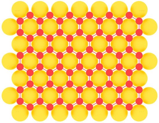
Figure 6.
Model of borophene layer on a metal substrate.
3.2. Group IVA Single-Element 2D Materials
Unlike graphene, a monolayer of carbon atoms with sp2-hybridization, which can be fabricated by simple exfoliation of single layers from graphite due to weak interlayer interaction, atom-thick layers of silicon, germanium, tin, or lead are not so readily exfoliated from the corresponding bulk materials because they have sp3-hybridization with strong covalent bonds. Consequently, the current task is to find methods of synthesis of transgraphenes other than exfoliation technique. Moreover, one of the basic methods of fabrication of silicene, germanene, stanene, and plumbene today is the heteroepitaxy on the surfaces matched by the lattice parameter [24].
For the first time, silicene was experimentally obtained by epitaxial methods in 2012 on Ag (111) substrate [20][21][20,21]. In this work, Ag(111) plates were cleaned by Ar+ sputtering with the energy 1.5 keV. Then, the substrates were annealed at the 500–600 °C to obtain atomically smooth silver surface. Silicon was deposited with the rate of 0.01–0.03 ML/min on the silver surface heated to 200–300 °C [20][21][20,21]. Later on, research on the growth of silicene on Ag(111) surface at various temperatures was carried out, and the important role of the substrate temperature in the formation of transgraphene structures was established [25]. It was shown that the number of defects in a honeycomb lattice increases with temperature, and silicene does not form at the temperatures of 330 °C or higher.
After that, silicene was synthesized on Ir(111) [24], Pb(111) [48], ZrB2(0001) [26], MoS2 [27], ZrC [28], Ru [29], and graphite [30] surfaces. For some substrates, to obtain uniform monolayer with honeycomb lattice, post-growth annealing of the synthesized structures was implemented. As in the previous case of single-element 2D materials of group IIIA, to serve a perfect surface for the group IVA buckled allotropes formation, the substrate should have lattice constant close to that of the desired 2D material, so that three of six atoms in the honeycomb mesh coincide with the nearest three atoms of the substrate (Figure 7).
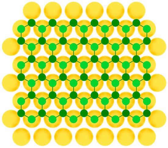
Figure 7.
Model of buckled silicene layer on a metal substrate (two colors are used for silicon atoms at different height positions).
3.3. Group VA Single-Element 2D Materials
Phosphorene was first produced by an exfoliation technique [98][103] and later fabricated in the method of molecular beam epitaxy on Au(111) substrate [99][104]. In work [99][104], clean Au(111) substrate was prepared by repeated Ar+ bombardment with ion energy of 1.5 keV at the pressure of about 1·10−5 Torr and subsequent annealing at 500 °C. Phosphorus was deposited by evaporation from a crucible containing bulk black phosphorus at 260 °C. During the deposition process, the substrate temperature was below 260 °C, so the initial growth stage involved the condensation of P4 molecules from the gas phase onto Au(111) surface. Then, the system was annealed at 250 °C for 60 min until well-defined monolayer phosphorus with a hexagonal structure appeared [99][104]. This was achieved due to the close lattice parameters of phosphorene and the substrate (Figure 8).
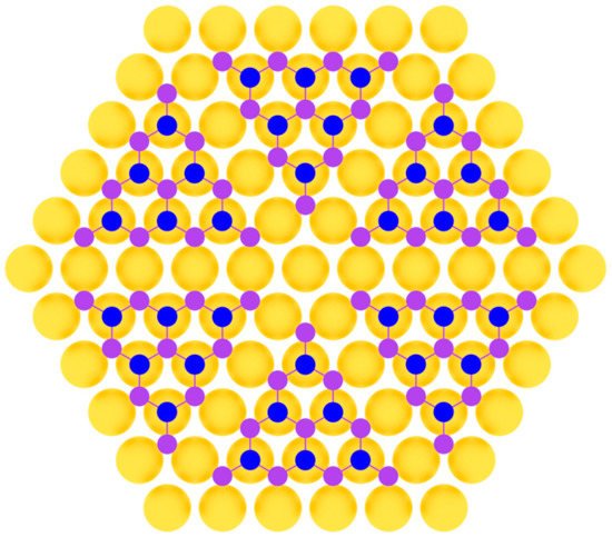
Figure 8.
Model of phosphorene layer on a metal substrate (two colors are used for phosphorus atoms at different height positions).
3.4. Group VIA Single-Element 2D Materials
To date, selenene was synthesized only by physical vapor deposition on Si(111) substrate in the work [100][118].
Tellurene was first obtained on flexible mica substrates by van der Waals epitaxy in 2014 in [101][119]. Thereafter, tellurium was successfully grown heteroepitaxially on highly oriented pyrolytic graphite [89] and graphene [102][120] (Figure 9).
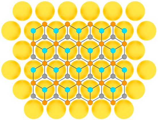
Figure 9.
Model of tellurene layer on a substrate (three colors are used for tellurium atoms at different height positions).