 +1 credit
| Version | Summary | Created by | Modification | Content Size | Created at | Operation |
|---|---|---|---|---|---|---|
| 1 | Lin-Qing Zhang | -- | 1618 | 2022-06-28 03:31:11 | | | |
| 2 | Conner Chen | -24 word(s) | 1594 | 2022-06-28 03:52:34 | | |
Video Upload Options
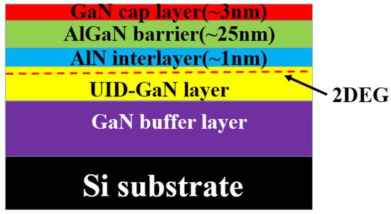
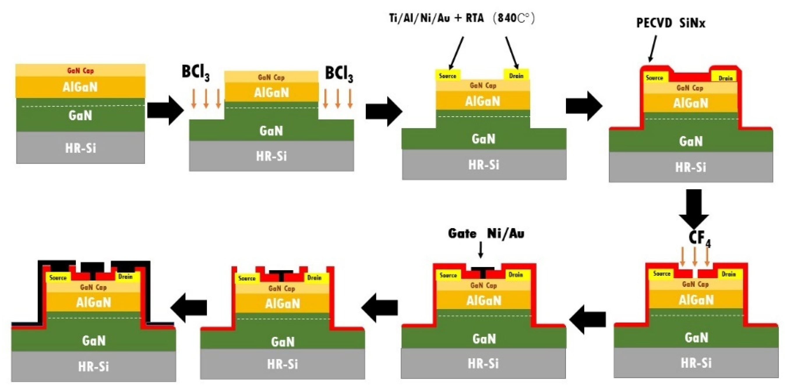
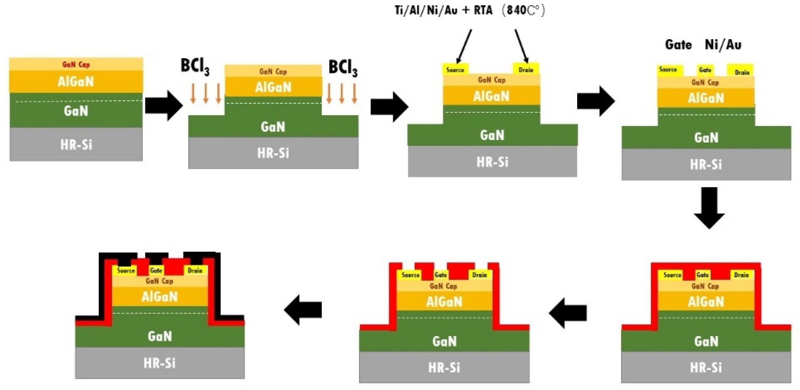
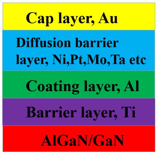
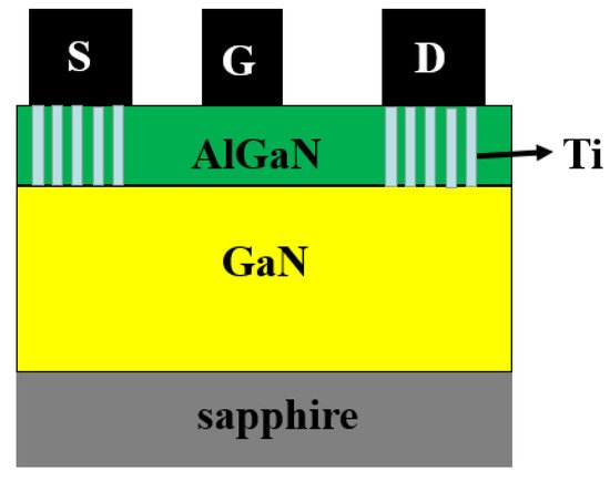
AlGaN/GaN high electron mobility transistors (HEMTs) are regarded as promising candidates for a 5G communication system, which demands higher frequency and power. Source/drain ohmic contact is one of the key fabrication processes crucial to the device performance. Firstly, Aucontained metal stacks combined with RTA high-temperature ohmic contact schemes were presented and analyzed, including process conditions and contact formation mechanisms. Considering the issues with the Au-contained technique, the overview of a sequence of Au-free schemes is given and comprehensively discussed. In addition, in order to solve various problems caused by hightemperature conditions, novel annealing techniques including microwave annealing (MWA) and laser annealing (LA) were proposed to form Au-free low-temperature ohmic contact to AlGaN/GaN HEMT. The most popular metallization schemes of ohmic contact in AlGaN/GaN HEMT is Ti/Al/X/Au, where X can be Ni, Mo, Pt, Ta, Ir, etc.
1. Introduction
2. Ti/Al/X/Au Au-Contained Ohmic Contact Technique
References
- Chen, K.J.; Häberlen, O.; Lidow, A.; lin Tsai, C.; Ueda, T.; Uemoto, Y.; Wu, Y. GaN-on-Si power technology: Devices and applications. IEEE Trans. Electron Devices 2017, 64, 779–795.
- He, J.; Cheng, W.C.; Wang, Q.; Cheng, K.; Yu, H.; Chai, Y. Recent Advances in GaN-Based Power HEMT Devices. Adv. Electron. Mater. 2021, 7, 2001045.
- Mishra, U.K.; Shen, L.; Kazior, T.E.; Wu, Y.F. GaN-based RF power devices and amplifiers. Proc. IEEE 2008, 96, 287–305.
- Palacios, T.; Chakraborty, A.; Rajan, S.; Poblenz, C.; Keller, S.; DenBaars, S.P.; Speck, J.S.; Mishra, U.K. High-power AlGaN/GaN HEMTs for ka-band applications. IEEE Electron Device Lett. 2005, 26, 781–783.
- Pengelly, R.S.; Wood, S.M.; Milligan, J.W.; Sheppard, S.T.; Pribble, W.L. A review of GaN on SiC high electron-mobility power transistors and MMICs. IEEE Trans. Microw. Theory Tech. 2012, 60, 1764–1783.
- Pérez-Tomás, A.; Fontserè, A.; Llobet, J.; Placidi, M.; Rennesson, S.; Baron, N.; Chenot, S.; Moreno, J.C.; Cordier, Y. Analysis of the AlGaN/GaN vertical bulk current on Si, sapphire, and free-standing GaN substrates. J. Appl. Phys. 2013, 113, 174501.
- Liang, Z.; Du, H.; Yuan, Y.; Wang, Q.; Kang, J.; Zhou, H.; Zhang, J.; Hao, Y.; Wang, X.; Zhang, G. Ultra-thin AlGaN/GaN HFET with a high breakdown voltage on sapphire substrates. Appl. Phys. Lett. 2021, 119, 252101.
- Ishida, M.; Ueda, T.; Tanaka, T.; Ueda, D. GaN on Si technologies for power switching devices. IEEE Trans. Electron Devices 2013, 60, 3053–3059.
- Wośko, M.; Szymański, T.; Paszkiewicz, B.; Pokryszka, P.; Paszkiewicz, R. MOVPE growth conditions optimization for AlGaN/GaN/Si heterostructures with SiN and LT-AlN interlayers designed for HEMT applications. J. Mater. Sci. Mater. Electron. 2019, 30, 4111–4116.
- Baliga, B.J. Power semiconductor device figure of merit for high-frequency applications. IEEE Electron Device Lett. 1989, 10, 455–457.
- Tang, Y.; Shinohara, K.; Regan, D.; Corrion, A.; Brown, D.; Wong, J.; Schmitz, A.; Fung, H.; Kim, S.; Micovic, M. Ultrahigh-speed GaN high-electron-mobility transistors with fT/fmax of 454/444 GHz. IEEE Electron Device Lett. 2015, 36, 549–551.
- Su, M.; Chen, C.; Rajan, S. Prospects for the application of GaN power devices in hybrid electric vehicle drive systems. Semicond. Sci. Technol. 2013, 28, 074012.
- Freedsman, J.J.; Egawa, T.; Yamaoka, Y.; Yano, Y.; Ubukata, A.; Tabuchi, T.; Matsumoto, K. Normally-off Al2O3/AlGaN/GaN MOS-HEMT on 8 in. Si with low leakage current and high breakdown voltage (825 V). Appl. Phys. Express 2014, 7, 041003.
- Egawa, T. Heteroepitaxial growth and power electronics using AlGaN/GaN HEMT on Si. In Proceedings of the 2012 International Electron Devices Meeting, San Francisco, CA, USA, 10–13 December 2012.
- Then, H.W.; Radosavljevic, M.; Agababov, P.; Ban, I.; Bristol, R.; Chandhok, M.; Chouksey, S.; Holybee, B.; Huang, C.Y.; Krist, B.; et al. GaN and Si Transistors on 300mm Si (111) Enabled by 3D Monolithic Heterogeneous Integration. In Proceedings of the 2020 IEEE Symposium on VLSI Technology, Honolulu, HI, USA, 16–19 June 2020; pp. 1–2.
- Asbeck, P.M.; Yu, E.T.; Lau, S.S.; Sullivan, G.J.; Van Hove, J.; Redwing, J. Piezoelectric charge densities in AlGaN/GaN HFETs. Electron. Lett. 1997, 33, 1230–1231.
- Katz, O.; Horn, A.; Bahir, G.; Salzman, J. Electron mobility in an AlGaN/GaN two-dimensional electron gas. I. Carrier concentration dependent mobility. IEEE Trans. Electron Devices 2003, 50, 2002–2008.
- Jessen, G.H.; Fitch, R.C.; Gillespie, J.K.; Via, G.; Crespo, A.; Langley, D.; Denninghoff, D.J.; Trejo, M.; Heller, E.R. Short-channel effect limitations on high-frequency operation of AlGaN/GaN HEMTs for T-gate devices. IEEE Trans. Electron Devices 2007, 54, 2589–2597.
- Ranjan, K.; Arulkumaran, S.; Ng, G.I.; Vicknesh, S. High Johnson’s figure of merit (8.32 THz· V) in 0.15-µm conventional T-gate AlGaN/GaN HEMTs on silicon. Appl. Phys. Express 2014, 7, 044102.
- Androse, D.R.; Deb, S.; Radhakrishnan, S.K.; Sekar, E. T-gate AlGaN/GaN HEMT with effective recess engineering for enhancement mode operation. Mater. Today Proc. 2021, 45, 3556–3559.
- Tasker, P.J.; Hughes, B. Importance of source and drain resistance to the maximum fT of millimeter-wave MODFETs. IEEE Electron Device Lett. 1989, 10, 291–293.
- Li, L.; Nomoto, K.; Pan, M.; Li, W.S.; Hickman, A.; Miller, J.; Lee, K.; Hu, Z.Y.; Bader, S.J.; Lee, S.M.; et al. GaN HEMTs on Si with regrown contacts and cutoff/maximum oscillation frequencies of 250/204 GHz. IEEE Electron Device Lett. 2020, 41, 689–692.
- Shinohara, K.; Corrion, A.; Regan, D.; Milosavljevic, I.; Brown, D.; Burnham, S.; Willadsen, P.J.; Butler, C.; Schmitz, A.; Wheeler, D.; et al. 220GHz fT and 400GHz fmax in 40-nm GaN DH-HEMTs with re-grown ohmic. In Proceedings of the 2010 International Electron Devices Meeting, San Francisco, CA, USA, 6–8 December 2010.
- Brown, D.F.; Shinohara, K.; Corrion, A.L.; Chu, R.; Williams, A.; Wong, J.C.; Rodriguez, I.A.; Grabar, R.; Johnson, M.; Butler, C.M.; et al. High-Speed, Enhancement-Mode GaN Power Switch with Regrown n+ GaN Ohmic Contacts and Staircase Field Plates. IEEE Electron Device Lett. 2013, 34, 1118–1120.
- Zhang, L.Q.; Huang, H.F.; Liu, X.Y.; Shi, J.S.; Liu, Z.; Zhao, S.X.; Wang, P.F. Two-dimensional device simulation for radio frequency performance of AlGaN/GaN HEMT, Semiconductor Technology International Conference. In Proceedings of the 2015 China Semiconductor Technology International Conference, Shanghai, China, 15–16 March 2015; pp. 1–3.
- Rickert, K.A.; Ellis, A.B.; Kim, J.K.; Lee, J.L.; Himpsel, F.J.; Dwikusuma, F.; Kuech, T.F. X-ray photoemission determination of the Schottky barrier height of metal contacts to n-GaN and p-GaN. J. Appl. Phys. 2002, 92, 6671–6678.
- Hirsch, M.T.; Duxstad, K.J.; Haller, E.E. Effects of annealing on Ti Schottky barriers on n-type GaN. Electron. Lett. 1997, 33, 95–96.
- Binari, S.C.; Dietrich, H.B.; Kelner, G.; Rowland, L.B.; Doverspike, K.; Gaskill, D.K. Electrical characterisation of Ti Schottky barriers on n-type GaN. Electron. Lett. 1994, 30, 909–911.
- Lee, M.L.; Sheu, J.K.; Lin, S.W. Schottky barrier heights of metal contacts to n-type gallium nitride with low-temperature-grown cap layer. Appl. Phys. Lett. 2006, 88, 032103.
- Reddy, V.R.; Ramesh, C.K.; Choi, C.J. Structural and electrical properties of Mo/n-GaN Schottky diodes. Phys. Status Solidi A 2006, 203, 622–627.
- Wu, Y.F.; Jiang, W.N.; Keller, B.P.; Keller, S.; Kapolnek, D.; Denbaars, S.P.; Mishra, U.K.; Wilson, B. Low resistance ohmic contact to n-GaN with a separate layer method. Solid-State Electron. 1997, 41, 165–168.
- Schmitz, A.C.; Ping, A.T.; Khan, M.A.; Chen, Q.; Yang, J.W.; Adesida, I. Metal contacts to n-type GaN. J. Electron. Mater. 1998, 27, 255–260.
- Luther, B.P.; Mohney, S.E.; Jackson, T.N.; Asif Khan, M.; Chen, Q.; Yang, J.W. Investigation of the mechanism for Ohmic contact formation in Al and Ti/Al contacts to n-type GaN. Appl. Phys. Lett. 1997, 7, 57–59.
- Ping, A.T.; Khan, M.A.; Adesida, I. Ohmic contacts to n-type GaN using Pd/Al metallization. J. Electron. Mater. 1996, 25, 819–824.
- Fan, Z.; Mohammad, S.N.; Kim, W.; Aktas, Ö.; Botchkarev, A.E.; Morkoç, H. Very low resistance multilayer Ohmic contact to n-GaN. Appl. Phys. Lett. 1996, 68, 1672–1674.
- Wang, L.; Mohammed, F.M.; Adesida, I. Differences in the reaction kinetics and contact formation mechanisms of annealed Ti/Al/Mo/Au Ohmic contacts on n-Ga N and AlGaN/GaN epilayers. J. Appl. Phys. 2007, 101, 013702.
- Luther, B.P.; Mohney, S.E.; Jackson, T.N. Titanium and titanium nitride contacts to n-type gallium nitride. Semicond. Sci. Technol. 1998, 13, 1322.
- Kim, J.K.; Jang, H.W.; Lee, J.L. Mechanism for Ohmic contact formation of Ti on n-type GaN investigated using synchrotron radiation photoemission spectroscopy. J. Appl. Phys. 2002, 91, 9214–9217.
- Van Daele, B.; Van Tendeloo, G.; Ruythooren, W.; Derluyn, J.; Leys, M.R.; Germain, M. The role of Al on Ohmic contact formation on n-type GaN and AlGaN/GaN. Appl. Phys. Lett. 2005, 87, 061905.
- Mohammed, F.M.; Wang, L.; Selvanathan, D.; Hu, H.; Adesida, I. Ohmic contact formation mechanism of Ta/Al/Mo/Au and Ti/Al/Mo/Au metallizations on AlGaN/GaN HEMTs. J. Vac. Sci. Technol. B Microelectron. Nanometer Struct. Processing Meas. Phenom. 2005, 23, 2330–2335.
- Qin, Z.X.; Chen, Z.Z.; Tong, Y.Z.; Ding, X.M.; Hu, X.D.; Yu, T.J.; Zhang, G.Y. Study of Ti/Au, Ti/Al/Au, and Ti/Al/Ni/Au ohmic contacts to n-GaN. Appl. Phys. A Mater. Sci. Processing 2004, 78, 729–731.
- Jacobs, B.; Kramer, M.; Geluk, E.J.; Karouta, F. Optimization of the Ti/Al/Ni/Au ohmic contact on AlGaN/GaN FET structures. J. Cryst. Growth 2002, 241, 15–18.
- Kong, X.; Wei, K.; Liu, G.; Liu, X. Role of Ti/Al relative thickness in the formation mechanism of Ti/Al/Ni/Au Ohmic contacts to AlGaN/GaN heterostructures. J. Phys. D Appl. Phys. 2012, 45, 265101.
- Feng, Q.; Li, L.M.; Hao, Y.; Ni, J.Y.; Zhang, J.C. The improvement of ohmic contact of Ti/Al/Ni/Au to AlGaN/GaN HEMT by multi-step annealing method. Solid-State Electron. 2009, 53, 955–958.
- Yu, H.; McCarthy, L.; Rajan, S.; Keller, S.; Denbaars, S.; Speck, J.; Mishra, U. Ion implanted AlGaN-GaN HEMTs with nonalloyed ohmic contacts. IEEE Electron Device Lett. 2005, 26, 283–285.
- Brown, D.F.; Williams, A.; Shinohara, K.; Kurdoghlian, A.; Milosavljevic, I.; Hashimoto, P.; Grabar, R.; Burnham, S.; Bulter, C.; Willadsen, P. W-band power performance of AlGaN/GaN DHFETs with regrown n+ GaN ohmic contacts by MBE. In Proceedings of the International Electron Devices Meeting, Washington, DC, USA, 5–7 December 2011.
- Yan, W.; Zhang, R.; Du, Y.; Han, W.; Yang, F. Analysis of the ohmic contacts of Ti/Al/Ni/Au to AlGaN/GaN HEMTs by the multi-step annealing process. J. Semicond. 2012, 33, 064005.
- Buttari, D.; Chini, A.; Meneghesso, G.; Zanoni, E.; Moran, B.; Heikman, S.; Zhang, N.Q.; Shen, L.; Coffie, R.; DenBaars, S.P.; et al. Systematic characterization of Cl2 reactive ion etching for improved ohmics in AlGaN/GaN HEMTs. IEEE Electron Device Lett. 2002, 23, 76–78.
- Recht, F.; McCarthy, L.; Rajan, S.; Chakraborty, A.; Poblenz, C.; Corrion, A.; Speck, J.S.; Mishra, U.K. Nonalloyed ohmic contacts in AlGaN/GaN HEMTs by ion implantation with reduced activation annealing temperature. IEEE Electron Device Lett. 2006, 27, 205–207.
- Wang, C.; He, Y.; Zheng, X.; Zhao, M.; Mi, M.; Li, X.; Mao, W.; Ma, X.; Hao, Y. Low ohmic-contact resistance in AlGaN/GaN high electron mobility transistors with holes etching in ohmic region. Electron. Lett. 2015, 51, 2145–2147.
- Fujishima, T.; Joglekar, S.; Piedra, D.; Lee, H.S.; Zhang, Y.; Uedono, A.; Palacios, T. Formation of low resistance ohmic contacts in GaN-based high electron mobility transistors with BCl3 surface plasma treatment. Appl. Phys. Lett. 2013, 103, 083508.
- Bright, A.N.; Thomas, P.J.; Weyland, M.; Tricker, D.M.; Humphreys, C.J.; Davies, R. Correlation of contact resistance with microstructure for Au/Ni/Al/Ti/AlGaN/GaN ohmic contacts using transmission electron microscopy. J. Appl. Phys. 2001, 89, 3143–3150.
- Boudart, B.; Trassaert, S.; Wallart, X.; Pesant, J.C.; Yaradou, O.; Théron, D.; Crosnier, Y.; Lahreche, H.; Omnes, F. Comparison between TiAl and TiAlNiAu ohmic contacts to n-type GaN. J. Electron. Mater. 2000, 29, 603–606.
- Mohammad, S.N. Contact mechanisms and design principles for nonalloyed ohmic contacts to n-GaN. J. Appl. Phys. 2004, 95, 4856–4865.
- Wang, L.; Mohammed, F.M.; Adesida, I. Formation mechanism of Ohmic contacts on AlGaN/GaN heterostructure: Electrical and microstructural characterizations. J. Appl. Phys. 2008, 103, 093516.
- Vertiatchikh, A.; Kaminsky, E.; Teetsov, J.; Robinson, K. Structural properties of alloyed Ti/Al/Ti/Au and Ti/Al/Mo/Au ohmic contacts to AlGaN/GaN. Solid-State Electron. 2006, 50, 1425–1429.

