AlGaN/GaN high electron mobility transistors (HEMTs) are regarded as promising candidates for a 5G communication system, which demands higher frequency and power. Source/drain ohmic contact is one of the key fabrication processes crucial to the device performance. Firstly, Aucontained metal stacks combined with RTA high-temperature ohmic contact schemes were presented and analyzed, including process conditions and contact formation mechanisms. Considering the issues with the Au-contained technique, the overview of a sequence of Au-free schemes is given and comprehensively discussed. In addition, in order to solve various problems caused by hightemperature conditions, novel annealing techniques including microwave annealing (MWA) and laser annealing (LA) were proposed to form Au-free low-temperature ohmic contact to AlGaN/GaN HEMT. The effects of the annealing method on surface morphology, gate leakage, dynamic onresistance (RON), and other device characteristics are investigated and presented in this paper. By using a low-temperature annealing atmosphere or selective annealing method, gate-first Si-CMOS compatible AlGaN/GaN HEMT technology can be realized for high frequency and power application.
1. Introduction
Traditional Si-based radio frequency (RF) and power devices, due to the physical limitation of Si material, cannot meet the requirements of higher-speed and higher-power in a 5G generation communication system. GaN-based HEMTs are regarded as promising candidates for high-frequency and high-power electronic devices due to their superior material properties [
1,
2,
3,
4]. The GaN-based materials are always heterogeneous and grown on other substrates, such as Si, SiC, and sapphire [
5,
6,
7,
8]. Among the heterojunction device structures, the AlGaN/GaN HEMT exhibits the best electronic characteristics [
9,
10,
11]. Furthermore, the AlGaN/GaN-on-Si is the structure most commonly selected for power application for the following reasons [
12,
13,
14,
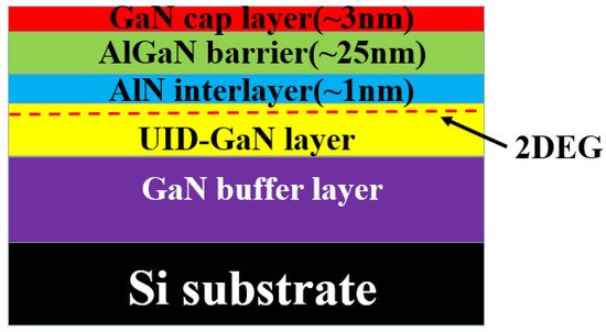
15]: the fabrication process is compatible with Si CMOS process flow, which helps to reduce the manufacturing cost. Realization of a large-size AlGaN/ GaN-on-Si wafer can also further reduce the cost. The regular epitaxial AlGaN/GaN layers are grown on a high-resistivity Si substrate by metal organic chemical vapor deposition (MOCVD), which is shown in
Figure 1. From Si bottom to top, a GaN buffer layer with a thickness of about 3 μm is deposited for reducing stress caused by lattice mismatch. After that, the device layer is formed by depositing an unintentional doped (UID) GaN device layer (~100 nm), AlN interlayer (~1 nm), and Al
xGa
1-xN barrier layer (~25 nm, x varies from 0.15–0.4). The two-dimensional electron gas (2DEG) is formed at the AlGaN/GaN interface due to the polarization effect [
16,
17]. Finally, the GaN cap layer (~3 nm) is deposited for protecting the device surface.
Figure 1. Schematic AlGaN/GaN-on Si device structure.
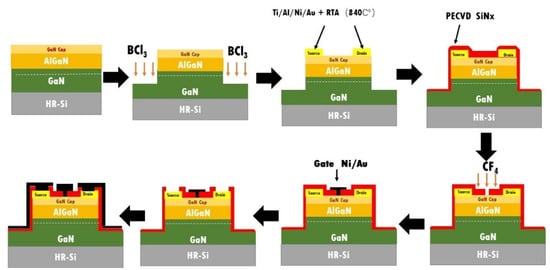
For RF application, the gate of the fabricated device is always formed in a T-shape for smaller gate resistance [
18,
19,
20]. The process flow, which can be seen in
Figure 2, consists of mesa isolation, source/drain ohmic contact formation, SiN passivation, T-shape gate formation, gate electrode deposition, via formation, and testing electrode deposition.
Figure 2. Schematic process flow of T-shaped AlGaN/GaN HEMT.
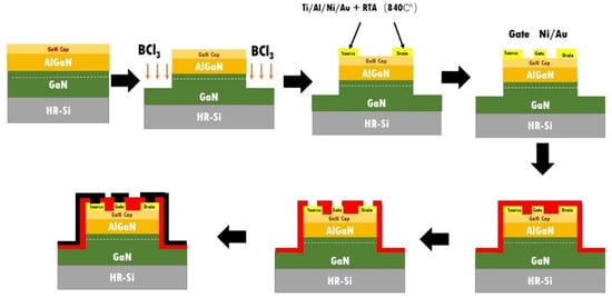
For power application, the gate is fabricated in a regular shape, as shown in Figure 3. The fabrication process consists of mesa isolation, source/drain ohmic contact formation, gate electrode deposition, SiN passivation, via formation, and testing electrode deposition.
Figure 3. Schematic process flow of regular AlGaN/GaN HEMT.
The quality of source/drain ohmic contact has a great impact on the performance of AlGaN/GaN HEMT, such as on-resistance (R
on), output current (I
DS), extrinsic transconductance (G
m), and current gain cut-off frequency (f
T) [
11,
21,
22,
23,
24,
25]. Always, the source/drain regions form ohmic contact to reduce R
ON and improve output current and f
T characteristics. Thus, the source/drain ohmic contact technique should be investigated. Over the years, researchers have systematically investigated ohmic contact to n
+-GaN and AlGaN/GaN for achieving low contact resistance (R
C).
2. Ti/Al/X/Au Au-Contained Ohmic Contact Technique
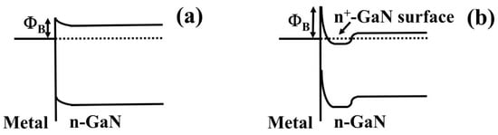
Considering the wide bandgap of (Al)GaN, two methods are adopted to form good quality ohmic contact: (1) reduce the barrier height(ΦB) by selecting the appropriate metal and (2) increase the possibility of tunneling by forming an n+-(Al)GaN surface. The energy band diagram of metal/(Al)GaN by two methods are shown in Figure 4.
Figure 4. Energy band diagram of metal/(Al)GaN by reducing the barrier height(ΦB) (a) and increasing the possibility of tunneling by forming n+-(Al)GaN surface (b).
For the first method, researchers selected Al, Ti, Au, Ni, Mo, Pd, Pt, Cr, etc. as contact metals and investigated their contact characteristics with (Al)GaN [
38,
39,
40,
41,
42,
43,
44,
45,
46]. The work function (W
m), specific contact resistivity (ρ
c), and Φ
B characteristics of different metal materials can be seen in
Table 1.
Table 1. Wm, ρc, ΦB characteristics of different metals to (Al)GaN.
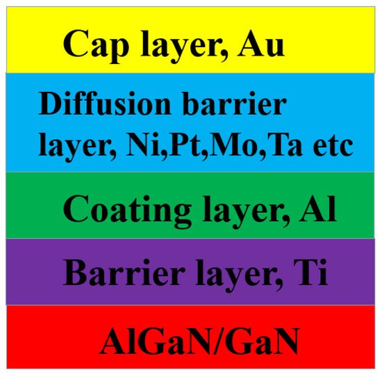
The results indicate that it is challenging to form good quality ohmic contact between single layer metal and (Al)GaN due to the higher W
m of the selected metal material. Also, the Ti, Al, etc. single layers are prone to oxidation during the high-temperature annealing process. Thus, a multilayer metal stack combined with a high-temperature annealing scheme became the common choice for GaN-based devices’ source/drain ohmic contact formation [
47]. The multilayer metal stack, as shown in
Figure 5, always consists of four metal layers: the barrier layer, coating layer, diffusion barrier layer, and cap layer. The most popular metal scheme is Ti/Al/X/Au, where X can be Ni, Mo, Pt, Ta, Ir, etc. During the annealing process, the barrier layer Ti reacts with the AlGaN layer to form TiN [
48]. TiN carries out lower work function [
49], which lowers the Schottky barrier height and therefore helps in ohmic contact formation. Also, the created N vacancies formed in the reaction process make the AlGaN layer underneath the contact metal n
+-doped, which makes electron tunneling easy for ohmic contact formation [
50]. Coating layer Al reacts with Ti under the high-temperature atmosphere to form Al
3Ti, which helps in ohmic contact formation [
51]. The diffusion layer Ni, Mo, Pt, and Ta etc., which owns high melt point prevents Au indiffusion and Al outdiffusion [
52]. Furthermore, the surface morphology of the contact metal can be affected by the metal layer. Au, which acts as a cap layer, prevents the Ti, Al layer oxidation within the high-temperature annealing atmosphere. Also, the Au layer improves the contact conductivity [
53].
Figure 5. Schematic structure of metal stacks used for forming ohmic contact to AlGaN/GaN HEMT.
Ohmic contact resistance R
C, ρ
c, surface morphology, and thermal stability are the important indexes of ohmic contact quality. The R
C value can be affected by the selected metal stack, the metal thickness, ohmic recessing of the AlGaN layer, surface pre-treatment prior to ohmic metallization, annealing time and temperature, n-type doped in the semiconductor, etc. [
52,
54,
55,
56,
57,
58,
59,
60,
61,
62,
63]. These affecting factors were investigated and optimized by universities and research institutions. Jacobs B et al. [
54] have systematically studied the influence of the metal stack, Ti, Al, Ni thickness, Ti/Al ratio, and annealing condition on R
C. In their results, the achieved optimized R
C is 0.2 Ω·mm with Ti thickness of 30 nm, Ti/Al ratio of 6, Ni thickness of 40 nm, and annealing temperature of 900 °C for 30 s. Yan et al. [
59] demonstrated that the R
C can be further reduced by a multi-step annealing process. With the improvement of AlGaN/GaN material growth, ohmic contact formation for metal and AlGaN/GaN becomes challenging. Buttari D et al. [
60] developed a low-damage Cl
2 reactive ion etching (RIE) recess etch on an AlGaN layer (7nm), decreasing R
C from 0.45 Ω·mm to 0.27 Ω·mm. By Si ion implantation in the source/drain region, Nomoto K et al. [
61] proved that the on-resistance can be decreased dramatically. By etching holes that were 0.8 μm × 0.8 μm in size and etching a depth of 10 nm, Wang et al. [
62] developed a pattern of square holes technique in the source/drain AlGaN layer and achieved an R
C as low as 0.1 Ω·mm, as shown in
Figure 6. The fabricated AlGaN/GaN HEMTs exhibits comparable output current, peak transconductance and threshold voltage characteristics with conventional AlGaN/GaN HEMTs. Before ohmic contact metal deposition, Fujishima T et al. [
63] developed a SiCl
4 and BCl
3 plasma treatment on the source/drain surface and achieved low R
C values of 0.41 Ω·mm and 0.17 Ω·mm, respectively. By optimizing the affecting factors of Ti/Al/X/Au schemes, the achieved R
C can be as low as 0.3 Ω·mm, and even much lower. The obtained low R
C can meet the requirements for the RF and power applications of AlGaN/GaN HEMT by using Ti/Al/Ni/Au metal schemes.
Figure 6. Schematic structure of AlGaN/GaN HEMT with holes etching in the ohmic region.
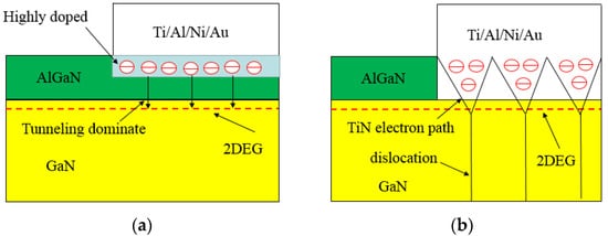
Universities and industries have conducted studies on the ohmic contact formation mechanism. Two methods are regarded as the mechanism to form ohmic contact to AlGaN/GaN HEMT: (1) a field emission (FE) tunneling mechanism [
64,
65,
66] via the formation of a thinner high doping or a lower barrier; and (2) a spike mechanism [
67,
68] by TiN direct electron path formation along the dislocation. In the FE tunneling mechanism, Ti reacts with the GaN or AlGaN layer to form TiN. N should be extracted from GaN or AlGaN, generating a highly n-doped interface region, which is responsible for the occurrence of FE tunneling. The work function of TiN (3.74 eV) is lower than Ti (4.33 eV), which is believed to lower the Schottky barrier for low-resistance ohmic contact formation. In the spike mechanism, the TiN projections forming along the dislocation places penetrate through the AlGaN layer under a high temperature, which sets up a direct electron path connecting the 2DEG and the ohmic metal. This method is believed to be more efficient in electron transferring than the FE tunneling mode. With the improvement of AlGaN/GaN material growth, the spike phenomenon, which penetrates through the whole AlGaN layer, becomes less likely to happen. The cross-sectional diagrams of both physical models are shown in
Figure 7, which reveals the ohmic contact formation mechanism.
Figure 7. Physical models of Ti/Al/Ni(x)/Au ohmic contact to AlGaN/GaN HEMT: FE tunneling mechanism (a) and spike mechanism (b).
This entry is adapted from the peer-reviewed paper 10.3390/cryst12060826