 +1 credit
| Version | Summary | Created by | Modification | Content Size | Created at | Operation |
|---|---|---|---|---|---|---|
| 1 | Hongnan Xu | + 3277 word(s) | 3277 | 2020-09-16 04:48:22 |
Video Upload Options
The multi-mode routing devices are used for transferring higher-order modes in the multi-mode bus waveguide without introducing mode-dependent losses or inter-modal crosstalk, including multi-mode bend, multi-mode crossing and multi-mode splitter.
1. Introduction
A complex topology is always desired to boost the performance of an on-chip data link. For example, Figure 1 shows the configuration for the multi-mode interconnects in a micro-processor with five cores. From the configuration, one can find that a situation has arisen where multi-mode routing devices are necessary to facilitate the multi-mode network; also, the multi-mode routing devices should fall into three categories: multi-mode bends, multi-mode crossings and multi-mode splitters.
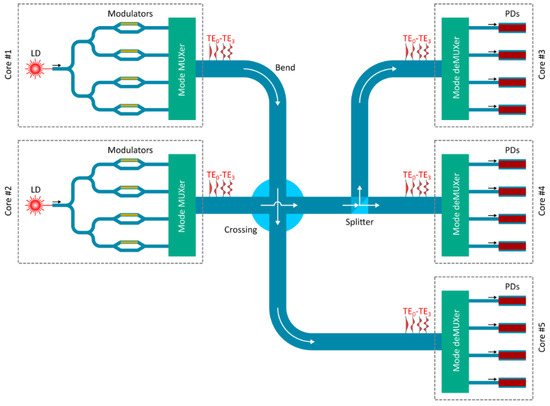
Figure 1. The configuration for MDM-enabled interconnects with multi-mode routing devices.
2. Silicon Multi-Mode Bends
The waveguide bend is a basic component that constitutes the cornerstone of a photonic integrated circuit. The SOI waveguide can support an extremely small bending radius, taking advantage of its ultra-high-index contrast. However, most of the reported silicon waveguide bends only work for the fundamental modes (i.e., TE0, TM0) since the higher-order modes are vulnerable in the bending section. The underlying reason is the significant inter-modal crosstalk (IMC) induced by the distinct modal profiles between straight/bent waveguides. Here, we give a calculation example to explain this phenomenon. Figure 2a shows the calculated field profiles for the first four TE and TM modes (i.e., TE0–3, TM0–3) in a straight multi-mode waveguide with a 220-nm thickness and 2-μm width. From the profiles, each straight-waveguide mode (SWM) has a symmetric power distribution over the core region. In contrast, the power distribution is asymmetric for each bent-waveguide mode (BWM), as shown in Figure 2b. Here, the bending radius is chosen to be 15 μm as an example. Thus, when the incident light meets the straight–bent junction, a single SWM will be decomposed into multiple BWMs, which will interfere with each other along the waveguide bend, leading to the significant IMC. The light propagation profiles are calculated for the multi-mode bend when TE0–3 and TM0–3 modes are launched, as shown in Figures 2c and 2d, where a strong inter-modal interference can be observed. Thus, one has to adopt an extremely large bending radius (typically > 200 μm) to relax the perturbation at the straight–bent junction and depress the undesired IMC. Over the past few years, great attention has been paid to developing multi-mode bending structures, including gradient index bends[1][2], mode converter-assisted bends[3][4], gradient curvature bends[5] and corner bends[6], as summarized in Figure 3.
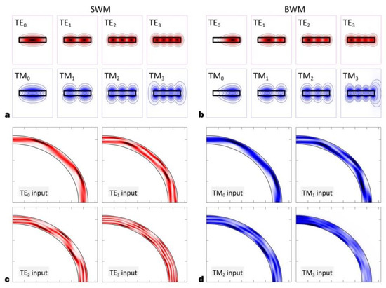
Figure 2. The calculated field profiles for (a) straight-waveguide mode (SWM) and (b) bent-waveguide mode (BWM). The calculated light propagation profiles for a 15-μm multi-mode bend when (c) TE0–3 and (d) TM0–3 modes are launched.
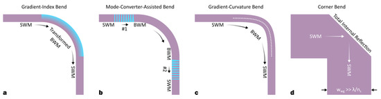
Figure 3. The schematics for different silicon multi-mode bends: (a) gradient index bend[1][2], (b) mode converter-assisted bend[3][4], (c) gradient curvature bend[5], (d) corner bend[6].
To eliminate the bending-induced IMC, the modal mismatch between SWMs and BWMs should be depressed. In 2012, L. H. Gabrielli et al. reported the first sharp multi-mode bend on silicon[1], as illustrated in Figure 13a. Transformation optics (TO) is utilized to map the lateral index profile. The transformed BWMs and SWMs have identical power distributions; thus, the incident higher-order modes will directly propagate through the multi-mode bend without any disturbance since the modal mismatch is eliminated. However, complicated grayscale lithography is needed to attain a non-uniform index distribution by pattering the thickness profile, leading to a CMOS-incompatible fabrication. Additionally, the bending radius is still quite large (≈78.8 μm). An improved design was proposed to overcome these obstacles[2]. For this design, the gradient index profile is generated by patterning a series of SWGs on the waveguide's top surface. The effective medium index can be precisely mapped by tailoring the SWG duty cycle. Furthermore, this novel structure can be easily fabricated by performing a simple shallow etching, which is a standard fabrication process in silicon photonics foundries. Such SWG-based multi-mode bends can provide low losses (IL < 0.7 dB), low crosstalk (IMC < −22 dB) and a broad bandwidth (BW > 80 nm) for the first three TE modes (i.e., TE0–2).
Alternatively, a multi-mode bend can also be realized by adopting a pair of mode converters, as shown in Figure 3b. The incident SWMs are firstly converted to the corresponding BWMs by converter #1; thus, the light transport in the multi-mode bend will not introduce any inter-modal interference. At the output port, the SWMs are then restored from the BWMs by converter #2. Therefore, the key issue is to realize the mode converter enabling SWM-BWM conversion with a low IMC. In [3], the authors optimized a SWM-BWM converter working for TE0 and TE1 modes. The bending radius is as small as 5 μm. The mode conversion efficiency could reach ≈100% by implementing a particle-swarm optimization (PSO) that defines the waveguide geometry. Low losses (IL < 0.2 dB), low crosstalk (IMC < −22 dB) and a broad bandwidth (BW > 100 nm) were experimentally demonstrated. However, this structure can only support two modes; meanwhile, the PSO process could be very time-consuming when a larger mode capacity is considered. Later, the SWG-based mode converter was proposed[4]. This converter consists of a multi-mode waveguide and a group of SWGs on the top-surface. The SWGs are non-uniform along both lateral and propagation directions, so the input SWMs can be gradually “pushed” to one sidewall, leading to the adiabatic conversion from SWMs to BWMs. Another identical mode converter is inserted at the output port to revert BWMs to SWMs. Such an SWG-based converter is able to support the first four TM modes (i.e., TM0–3) with a sharp bending radius of 30 μm. The losses and crosstalk were measured to be IL < 1 dB and IMC < −20 dB over a broad wavelength band from 1.52 μm to 1.60 μm (BW > 80 nm).
Multi-mode bends also need to be fabrication-friendly, given that the bending structures are recurring in the MDM system. However, the aforementioned designs usually require complex index mapping with subwavelength structures. A more convenient and robust scheme is based on the gradient curvature bend[5], as shown in Figure 3c. The idea is to engineer the bending trajectory by using some special curves with variant curvature, such as spline or Euler curves. For a Euler bend, the curvature is minimal at the input/output port, and adiabatically reaches its maximum value at the middle point. Thus, the inter-modal coupling can be efficiently inhibited as long as the curvature gradient is small enough. By using this method, low losses (IL < 0.5 dB), low crosstalk (IMC < −20 dB) and a broad bandwidth (BW > 90 nm) can be achieved for the first four TM modes (i.e., TM0–3). The effective radius is also as small as 45 μm. Actually, such gradient curvature bends can be regarded as special forms of mode converter-assisted bends, except that the “mode converters” are merged into the bending section, so that the footprint can be reduced. Another simple scheme is based on the corner bend[6], as illustrated in Figure 3d. The idea is to simultaneously change the propagation directions for all the supported modes at an inclined Si-SiO2 interface, where total internal reflection (TIR) happens. The corner bend is intrinsically lossless and crosstalk free (IL < 0.5 dB, IMC < −20 dB) since there is no SWM-BWM conversion. In theory, the working bandwidth can be as large as >420 nm and the capacity can be scaled up to ten modes. However, it should be noted that the core width has to be wide enough (typically >10 μm) to lower the diffraction losses at the corner junction; thus, one has to use two additional mode size converters (e.g., adiabatic tapers) as connectors between the bus waveguide and corner bend.
3. Silicon Multi-Mode Crossings
Waveguide crossing plays an important role in the photonic integrated circuit, with a complex pathway topology. Over the past few years, various single-mode waveguide crossings have been reported, including ones based on MMIs[7], ridge expanders[8], inter-layer couplers[9] and subwavelength structures[10]. Among them, the MMI-based crossing is most commonly used due to its simple design, compact size (<10 × 10 μm2) and low insertion losses (IL < 0.2 dB). The MMI can serve as a waveguide-lens that focuses the incident light at the cross-over position, which effectively reduces the diffraction losses. However, such a focusing process only works for a single fundamental mode. To explain this, we show a calculation example considering the first two TE modes (i.e., TE0, TE1), as shown in Figure 4. The focal length of MMI is basically determined by interference-induced self-imaging, which can be formulated as:
|
Lf,0 = LB,0 = λ/(neff,TE0- neff,TE2) |
(5) |
|
Lf,1 = LB,1 = λ/(neff,TE1- neff,TE3) |
(6) |
where Lf,i is the focal length for TEi, LB,i is the beat length for TEi, neff,TEi is the TEi effective index, λ is the working wavelength. We calculate the beat lengths for TE0 and TE1 with varied waveguide width (wwg) using Equations (5) and (6), as shown in Figure 4a. Here, the waveguide thickness is chosen to be hwg = 220 nm, while the working wavelength is set to be λ = 1.55 μm. We also calculate the light propagation profiles for the MMI-based crossings with Lf optimized for TE0 and TE1, as shown in Figure 4b. It can be seen that the beat lengths are always different between TE0 and TE1 regardless of the variant waveguide widths. Consequently, it is challenging to focus multiple modes at the same cross-over position.
Some works suggest that the multi-mode cross-over propagation could be simply realized by employing a direct-crossing structure[11], since the beam divergence is negligible with a wide waveguide, enabling a lossless multi-mode transport (see Figure 5a). To achieve this, the waveguide width (wwg) should be:
|
wwg >> λ/ns |
(7) |
where ns is the effective index for the slab mode, λ is the working wavelength. For instance, to support a four-mode cross-over (e.g., TE0–3), the waveguide width should be chosen as wwg > 10 μm. On the other hand, the multi-mode bus waveguide is usually quite narrow (e.g., wwg < 2 μm); thus, the long adiabatic tapers (typically > 100 μm) should also be involved to convert the mode size, leading to an extremely large total device size (>200 μm). It is crucial that the crossing structures should have small footprints (<20 μm) to fit in the dense cross-bar networks. In this regard, such a direct crossing is not applicable for practical uses unless the taper length can be effectively shrunk to ≈10 μm.
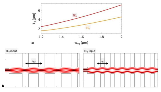
Figure 4. (a) The calculated beat lengths (LB) for TE0 and TE1 modes with varied waveguide width (wwg). (b) The calculated light propagation profiles for MMI-based crossings when TE0 (left panel) and TE1 (right panel) are launched. The beat lengths are different between TE0 and TE1.
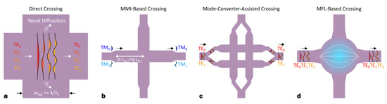
Figure 5. The schematics for different silicon multi-mode crossings: (a) direct crossing[11], (b) MMI-based crossing[12][13], (c) mode converter-assisted crossing[14][15], (d) Maxwell's fisheye lens (MFL)-based crossing[16][17].
A multi-mode crossing with a reduced size was firstly reported in 2016[12], as shown in Figure 5b. The proposed scheme is still based on the MMI structure, but the focal length is chosen to be the common multiple of beat lengths for TM0 and TM1:
|
Lf = p·LB,0 = q·LB,1 |
(8) |
|
LB,0 = λ/(neff,TM0- neff,TM2) |
(9) |
|
LB,1 = λ/(neff,TM1- neff,TM3) |
(10) |
where p and q are two integers, Lf is the focal length, LB,i is the beat length for TMi, neff,TMi is the TMi effective index. In this way, light focusing can be simultaneously achieved for TM0 and TM1. The measurement results exhibit insertion losses of IL ≈ 1.5 dB and crosstalk of XT < −18 dB. The working performances can be further improved by cascading several multi-sectional taper structures (IL ≈ 0.1 dB, XT < −30 dB)[13]. However, there are two major drawbacks for the MMI-based crossings: first, the device size is still relatively large (≈30 × 30 μm2) since the focal length is multiplied; second, the capacity is restricted to two modes, because it is tough to find the common multiple of beat lengths for a large number of higher-order modes.
Another type of multi-mode crossing is based on mode converters. In [14], a two-mode crossing was proposed by using a 2 × 2 single-mode waveguide crossing matrix cascaded with four symmetric Y-junctions, as illustrated in Figure 5c. For such a scheme, the input TE0/TE1 modes are converted to the symmetric/asymmetric super-modes (i.e., TES/TEAS) in the Y-junction, so that all the crossing structures only need to work with TE0. The footprint is quite small (≈21 × 21 μm2), but the insertion losses are significant (IL ≈ 1.82 dB) owing to the intrinsically strong scattering at the junction tip. In [15], the similar idea was implemented to realize a three-mode crossing by using a 3 × 3 crossing matrix cascaded with four asymmetric Y-junctions. The insertion losses and crosstalk were measured to be IL < 0.9 dB, XT < −24 dB, respectively. Nevertheless, the mode capacity is still quite limited for this type of multi-mode crossing since higher-order mode conversion is difficult to realize.
Maxwell's fisheye lens (MFL) is a perfect imaging instrument with a gradient index map that focuses rays emanating from a point on the boundary to a conjugate point on the opposite side. In [16], an MFL-based multi-mode crossing was proposed and demonstrated, as shown in Figure 5d. In this work, MFL is constructed on a silicon slab based on the following equation:
|
neff(R) = nmax/[1 + (R/R0)2] |
(11) |
where neff(R) is the index distribution, nmax Is the maximum index, R0 is the maximum radius. To realize the gradient index map, the silicon slab is covered by a layer of metamaterial film comprised of a two-dimensional array of nano-rods whose effective medium index can be controlled by varying the nano-rod filling factor. Due to the perfect-imaging feature of MFL, the incident light will propagate through the crossing section and then form its self-image regardless of the mode order, so that all the input modes can be preserved throughout the crossing section. This MFL-based crossing can provide low losses (IL < 0.3 dB) and low crosstalk (XT < −20 dB) for the first two TM modes (i.e., TM0, TM1). The footprint is also as small as 18 × 18 μm2. Later, another MFL-based three-mode crossing was reported based on the grayscale lithography technology[17]. The MFL-based crossing is considered as a universal and scalable scheme that could work for any higher-order mode since the imaging process is independent from the mode order. Moreover, conjugate imaging of MFL also enables multiple cross-over pathways at a single junction, which allows for a multi-port star-crossing with an enhanced integration density.
4. Silicon Multi-Mode Splitters
Single-mode power splitting can be easily realized by exploiting Y-junctions[18], directional couplers[19] and MMI couplers[20]. However, these approaches cannot be directly employed in the multi-mode regime, because there are two underlying constraints for multi-mode power splitting: first, the splitting ratios (SRs) should be equivalent for all the input modes; second, the mode order should be preserved. The simplest case is a symmetric Y-junction, where the input TE1 mode will convert to a pair of TE0 modes in two branches, as shown in Figure 16. Hence, the Y-junction cannot serve as a multi-mode power splitter since the mode order is changed. Recently, a variety of multi-mode splitters have been reported, including ones based on directional couplers[21], adiabatic couplers[22], mode converter-assisted Y-junctions[23] and SWG transflectors[24], as summarized in Figure 7.
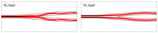
Figure 6. The calculated light propagation profiles for a Y-junction when TE0 (left panel) and TE1 (right panel) are launched. The mode order cannot be preserved in the splitting process.
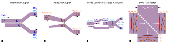
Figure 7. The schematics for different silicon multi-mode splitters based on (a) directional coupler[21], (b) adiabatic coupler[22], (c) mode converter-assisted Y-junction[23], (d) subwavelength grating (SWG) transflector[24].
The first silicon multi-mode power splitter was designed based a directional coupler[21], as shown in Figure 7a. The incident modes (i.e., TM0, TM1) can be partially transferred to the adjacent waveguide with evanescent coupling. The problem is that the half-beat lengths are distinct for different mode orders. Thus, one has to carefully choose the structural parameters to ensure that the coupling length satisfies the following equation:
|
Lc = (1/2 + p)·Lπ,0 = (1/2 + q)·Lπ,1 |
(12) |
where p and q are two integers, Lc is the coupling length, Lπ,i is the half-beat length for TMi. Here, Lπ,i can be obtained by using the super-mode theorem. In this way, both TM0 and TM1 modes can be allocated to two waveguides with the same splitting ratio of SR = 50%. For the fabricated device, the insertion losses and crosstalk were measured to be IL < −0.7 dB and XT < −14.3 dB, respectively. The major disadvantage is the narrow bandwidth (BW < 30 nm) since Lπ,i is strongly wavelength dependent. Moreover, this approach is not scalable, because it is difficult to find an optimal parameter for more than two modes. As an improvement, the adiabatic coupler was proposed to enhance the bandwidth and expand the capacity[22]. The input modes are firstly converted to the corresponding super-modes, which are then evenly split by a symmetric Y-junction, as shown in Figure 7b. In theory, this adiabatic coupler-based structure can provide an ultra-broad bandwidth (BW > 165 nm) as well as an arbitrarily large capacity. The insertion losses and crosstalk are also quite low (IL < 0.12 dB, XT < −18.5 dB). However, for this scheme, the coupling length has to be extremely long (> 800 μm) to meet the adiabatic condition. In[23], the mode converter-assisted Y-junction was proposed to realize a scalable multi-mode splitter with a smaller footprint as well as a broad bandwidth. The input TMi is firstly converted to the TM2i+1 mode as a transition, which is then divided into two beams and reverted to the TMi mode through a symmetric Y-junction, as shown in Figure 7c. The TMi-TM2i+1 conversion can be achieved for any higher-order mode by bridging two groups of cascaded ADCs. Based on this scheme, the device footprint can be reduced to ≈120 μm. The measurement results show low losses (IL < 0.86 dB) and low crosstalk (XT < −15.7 dB). For the aforementioned multi-mode splitters, the splitting ratio is fixed to SR = 50% (i.e., 3-dB power splitting). However, an arbitrary splitting ratio is commonly required for a wide scope of applications, e.g., power distribution, power monitoring and box-like filtering. Hence, it is also very important to develop multi-mode splitters with a splitting ratio beyond 50:50.
In [24], an ultra-broadband silicon multimode splitter with an arbitrary splitting ratio was proposed for the first time, as shown in Figure 7d. The structure is a direct crossing with an obliquely embedded SWG that partially reflects the incident modes. The SWG is formed by a one-dimensional array of subwavelength nano-holes that can be collectively regarded as an effective medium transflector. The reflectance can be almost the same for all the input modes (i.e., TE0–2) since the effective indices are quite close when w0 >> λ/ns. More importantly, any desired splitting ratio, ranging from 0% to 100%, can be achieved by simply changing the SWG duty cycle. Additionally, the splitting ratio spectra can be very uniform over an extremely broad bandwidth (BW > 415 nm) covering O-, E-, S-, C-, L- and U-bands. The insertion losses and crosstalk are also quite low (IL < 0.1 dB, XT < −20 dB). A four-mode power splitter was also realized by using a uniform trench as a transflector, whose splitting ratio can also be modified by tuning the trench width[11].
5. Overview
In general, the major issue for realizing high-performance multi-mode routing devices is to lower the mode-dependent-losses as well as the inter-modal crosstalk. For multi-mode bend, one need to eliminate the mode mismatch between straight waveguide modes and bent waveguide modes to inhibit the mode coupling at the straight-bent junction. For multi-mode crossing, the goal is to form self-images for all the input modes at the same postion. The Maxswell's fisheye lens could be useful to tackle this problem. For multi-mode splitter, one has to make sure that the mode orders are maintained after splitting, which could be obtained by introducing the SWG-based transflectors.
References
- Lucas H. Gabrielli; David Liu; S. G. Johnson; Michal Lipson; On-chip transformation optics for multimode waveguide bends. Nature Communications 2012, 3, 1217, 10.1038/ncomms2232.
- Hao Wu; Chenlei Li; Lijia Song; Hon-Ki Tsang; John E. Bowers; Daoxin Dai; Ultra-Sharp Multimode Waveguide Bends with Subwavelength Gratings. Laser & Photonics Review 2019, 13, 1800119, 10.1002/lpor.201800119.
- Chunlei Sun; Yu Yu; Guanyu Chen; Xinliang Zhang; Guanyu Chen And Xinliang Zhang; Ultra-compact bent multimode silicon waveguide with ultralow inter-mode crosstalk. Optics Letters 2017, 42, 3004-3007, 10.1364/ol.42.003004.
- Hongnan Xu; Yaocheng Shi; Ultra-Sharp Multi-Mode Waveguide Bending Assisted with Metamaterial-Based Mode Converters. Laser & Photonics Review 2018, 12, 1700240, 10.1002/lpor.201700240.
- Xiaohui Jiang; Hao Wu; Daoxin Dai; Low-loss and low-crosstalk multimode waveguide bend on silicon. Optics Express 2018, 26, 17680-17689, 10.1364/oe.26.017680.
- Yi Wang; Daoxin Dai; Multimode silicon photonic waveguide corner-bend.. Optics Express 2020, 28, 9062-9071, 10.1364/OE.387978.
- Howard R. Stuart; Waveguide lenses with multimode interference for low-loss slab propagation.. Optics Letters 2003, 28, 2141-2143, 10.1364/ol.28.002141.
- Wim Bogaerts; Pieter Dumon; Dries Van Thourhout; Roel Baets; Low-loss, low-cross-talk crossings for silicon-on-insulator nanophotonic waveguides. Optics Letters 2007, 32, 2801-2803, 10.1364/ol.32.002801.
- Andrei V. Tsarev; Efficient silicon wire waveguide crossing with negligible loss and crosstalk.. Optics Express 2011, 19, 13732-13737, 10.1364/oe.19.013732.
- Przemek J. Bock; Pavel Cheben; Jens H. Schmid; Jean Lapointe; André Delâge; Dan-Xia Xu; Siegfried Janz; Adam Densmore; Trevor J. Hall; Subwavelength grating crossings for silicon wire waveguides.. Optics Express 2010, 18, 16146-16155, 10.1364/oe.18.016146.
- Chunlei Sun; Yunhong Ding; Zhen Li; Wei Qi; Yu Yu; Xinliang Zhang; Key Multimode Silicon Photonic Devices Inspired by Geometrical Optics. ACS Photonics 2020, 7, 2037-2045, 10.1021/acsphotonics.0c00370.
- Hongnan Xu; Yaocheng Shi; Dual-mode waveguide crossing utilizing taper-assisted multimode-interference couplers. Optics Letters 2016, 41, 5381-5384, 10.1364/ol.41.005381.
- Beibei Wu; Yu Yu; Xinliang Zhang; Wu Beibei; Multimode waveguide crossing with ultralow loss and low imbalance. Optics Express 2020, 28, 14705-14711, 10.1364/oe.392445.
- Xinliang Zhang; Ultra-compact waveguide crossing for a mode-division multiplexing optical network. Optics Letters 2017, 42, 4913, 10.1364/OL.42.004913.
- Weijie Chang; Luluzi Lu; Xinshu Ren; Longhui Lu; Mengfan Cheng; Deming Liu; Minming Zhang; An Ultracompact Multimode Waveguide Crossing Based on Subwavelength Asymmetric Y-Junction. IEEE Photonics Journal 2018, 10, 1-8, 10.1109/jphot.2018.2847762.
- Hongnan Xu; Yaocheng Shi; Metamaterial-Based Maxwell's Fisheye Lens for Multimode Waveguide Crossing. Laser & Photonics Review 2018, 12, 1800094, 10.1002/lpor.201800094.
- Shuyi Li; Yangyang Zhou; Jianji Dong; Xinliang Zhang; Eric Cassan; Jin Hou; Chunyong Yang; Shaoping Chen; Dingshan Gao; Huanyang Chen; et al. Universal multimode waveguide crossing based on transformation optics. Optica 2018, 5, 1549-1556, 10.1364/optica.5.001549.
- Yi Zhang; Shuyu Yang; Andy Eu-Jin Lim; Guo-Qiang Lo; Christophe Galland; Tom Baehr-Jones; Michael Hochberg; A compact and low loss Y-junction for submicron silicon waveguide.. Optics Express 2013, 21, 1310-1316, 10.1364/oe.21.001310.
- Robert Halir; A. Maese-Novo; Alejandro Ortega-Moñux; I. Molina-Fernández; J. Gonzalo Wangüemert-Pérez; P. Cheben; D.-X. Xu; J. H. Schmid; S. Janz; Colorless directional coupler with dispersion engineered sub-wavelength structure.. Optics Express 2012, 20, 13470-13477, 10.1364/oe.20.013470.
- D. J. Thomson; Y. Hu; G. T. Reed; Jean-Marc Fedeli; Low Loss MMI Couplers for High Performance MZI Modulators. IEEE Photonics Technology Letters 2010, 22, 1485-1487, 10.1109/LPT.2010.2063018.
- Yuchan Luo; Yu Yu; Mengyuan Ye; Chunlei Sun; Xinliang Zhang; Integrated dual-mode 3 dB power coupler based on tapered directional coupler. Scientific Reports 2016, 6, 23516, 10.1038/srep23516.
- Liangshun Han; Bill P.-P. Kuo; N. Alic; S. Radic; Ultra-broadband multimode 3dB optical power splitter using an adiabatic coupler and a Y-branch. Optics Express 2018, 26, 14800-14809, 10.1364/oe.26.014800.
- Hongnan Xu; Yaocheng Shi; Ultra-broadband dual-mode 3 dB power splitter based on a Y-junction assisted with mode converters. Optics Letters 2016, 41, 5047-5050, 10.1364/ol.41.005047.
- Hongnan Xu; Daoxin Dai; Yaocheng Shi; Ultra-broadband on-chip multimode power splitter with an arbitrary splitting ratio. OSA Continuum 2020, 3, 1212, 10.1364/osac.396024.
- Hongnan Xu; Daoxin Dai; Yaocheng Shi; Ultra-broadband on-chip multimode power splitter with an arbitrary splitting ratio. OSA Continuum 2020, 3, 1212, 10.1364/osac.396024.

