 +1 credit
| Version | Summary | Created by | Modification | Content Size | Created at | Operation |
|---|---|---|---|---|---|---|
| 1 | Paul Chinonso Uzoma | + 1967 word(s) | 1967 | 2020-09-21 06:01:04 | | | |
| 2 | Nicole Yin | -1 word(s) | 1966 | 2020-09-28 04:36:29 | | |
Video Upload Options
Materials can be rightly characterized as 2D material or nanosheet if only one of its dimensions is in nano-size, they usually resemble a large sheet with one or few atomic thickness layers (more like a sheet of paper).
This explains the fundamental characteristic of 2D materials and their unique properties that made them very attractive in tribological applications. Also, the method of preparation of the materials are highlighted.
1. Introduction
Since their discovery, they have undoubtedly attracted great academic and industrial interests due to their magnificent array of electronic, optical, physical and chemical properties, which are absent in their bulk counterparts[1].
2. Characteristics of 2D Materials
These unique features are a result of the effect of their spatial confinement in one dimension[2]. Besides, since nanosheets are atomically thin and possess strong in-plane bonds, they are liable to exhibit a remarkable combination of thermal, high mechanical strength and flexibility which are desirable properties for use in various devices[3], which can also result to unusual frictional features[4][5]. The high degree of flexibility associated with 2D materials whenever they are in contact with nearby objects plays a vital role in deciding the real contact area and the frictional pinning potential[6][7]. Besides, the dispersion of 2D materials in aqueous solution are suitable precursors for the design of 2D based films[8], and since all atoms of 2D materials are surface atoms, this provides a proper handle to change the properties of the materials through surface functionalization and modification[9][10].
Notably, layered materials such as graphene, MoS2, WS2 and hexagonal BN (h-BN) have long been employed as solid lubricants in numerous engineering applications. The outstanding lubrication performance of these bulk materials is known to be due to the weak interlayer interaction and easy sliding between surrounding atomic layers[11][12]. Recent nanoscale experiments have revealed that layered materials, down to one atomic layer, also show outstandingly low surface friction when they are slid against other counter surfaces[6][12]. Besides weak interlayer interaction, regular atomic arrangements are also known to impact these materials with the potential to achieve super-low friction, otherwise known as superlubricity[13][14]. Moreover, regarding few-layered 2D materials, it has been shown that the static frictional force gradually increases for a few initial atomic periods before reaching a steady value. Such fleeting behavior and the associated improvement of the steady-state of friction, decreases as the number of 2D layer increases and was observed only when the 2D material was loosely attached to a substrate[7][15]. By employing atomistic simulations, Li et al. reproduce the experimental findings on layer-dependent friction and transient frictional strengthening on graphene nanosheets[7]. Atomic force analysis proved that the evolution of static friction is a demonstration of the innate tendency for thinner and less-constrained graphene to re-arrange its configuration as a direct effect of its higher flexibility. The tip atoms become more firmly pinned and reveal higher synchrony in their stick-slip character. While the quantity of atomic-scale contacts which is the real contact area expands, the local pinning state of individual atoms and the comprehensive commensurability also grows in frictional sliding on graphene nanosheets. Lee et al.[15] analyzed the nanotribological properties of some selected 2D materials such as graphene, MoS2, h-BN and niobium diselenide (NbSe2) which were separated from their bulk sources using mechanical exfoliation method. It was shown that friction on all the four 2D materials is greater than that of their bulk sources. Their study indicates that the higher friction is associated with the low bending stiffness of the thinnest layers known as the puckering effect. They employed a simple model of a tip sliding across an elastic membrane to understand the mechanism of the sheet stiffness in friction. Herein, when the tip comes in contact with the top surface, there is usually a local puckering because of adhesion[16], this is due to the low bending stiffness of the sheet in relation to its in-plane stiffness. The puckered geometry will be adjusted at the front edge by tip-sheet friction. This out-of-plane puckering might explain the increased friction due to the resultant increase in the tip-sheet contact area. Moreover, it can be due to the extra work required to shift the puckered region. As the sheet becomes thinner, the puckering effect becomes more significant. Besides, graphene, MoS2 and h-BN possess much lower friction (~1 nN) than NbSe2 (~7 nN). Zhou et al.[17] also demonstrated that TMDCs (MoS2, WS2, MoSe2, WSe2) having smaller vertical interlayer force constant, which is lower elastic modulus, shows more considerable friction when colliding against AFM tips. Furthermore, it is generally known that the kinetic energy during frictional sliding is released electronically or phononically[18][19]. Hence, contrary to what is obtained in bulk lubricants, the unique electrical (or electron-phonon coupling) of 2D materials is considered to have an impact on their frictional behavior[6].
In Summary, the frictional action mechanisms of 2D materials can be described as follows; firstly, because of the very tiny nature of nanosheets, it can penetrate the interspaces of the rubbing surfaces. Under normal force, the relative motion of the rubbing surfaces will provide the needed shear stress leading to the sliding of the interlayers of the nanosheets, thereby reduction of friction and wear. Secondly, there will be a formation of tribofilm at the contact area of sliding surfaces[20][21]. Initially, the formed tribofilm serves as a protective film separating the two rubbing surfaces from direct contact. However, as sliding continues and more heat is generated, a tribochemical reaction is triggered at the contact surfaces between the lubricants and the substrate, this will lead to the rupturing of the protective film and reformation of a new film[22]. This new film is known to significantly enhance tribological behavior[23]. Besides, the high temperature developed during sliding could melt the nanosheets enabling them to fill up the micro-holes, gaps and the concave areas in the contact surfaces, thereby reducing friction and wear[24].
3. Synthesis of 2D Materials
3.1. Mechanical Exfoliation
Over the years, several techniques including mechanical exfoliation, liquid-phase exfoliation, shear exfoliation, epitaxial growth of SiC, unzipping carbon nanotubes and chemical vapor deposition (CVD) have been explored for the synthesis of 2D materials. In 2004, micromechanical cleavage, also known as mechanical exfoliation, was first introduced as an efficient way to produce atomically thin graphene[25]. Using this technique, single-layer graphene was successfully cleaved from small crystals of highly oriented pyrolytic graphite (HOPG) with the aid of scotch tape, as shown in Figure 1a. The mechanics involve exerting a normal force on a scotch tape, which is applied to the HOPG surface. By continuously repeating this normal force, the graphitic layer gradually thins out until it becomes single-layer graphene from their parent layered bulk crystals[26][27]. This method has also been widely employed in the synthesis of other 2D materials, including TMDCs, h-BN and NbSe2[28][29][30][31]. The outstanding crystal quality with minimal defects make the mechanically cleaved ultrathin 2D materials desired candidates for fundamental study of their inherent physical, optical and electronic properties, and their use in high-performance electronic and/or optoelectronic devices such as transistors and phototransistors. Even though this method is simple and practicable, it is faced with the challenge of non-scalability because of meager output yield and slow output rate. Besides, the process is manually controlled; hence, precision and reproducibility in terms of shape, size and thickness is an enormous challenge[26]. Several researchers have modified the micromechanical cleavage, Shmavonyan and co-workers successfully synthesized monolayer graphene with a larger surface area by additionally separating few-layer graphene near the monolayer region as shown in Figure 1b,c[32]. Moreover, other modifications have been proposed, as described by Peng et al. [33] and Zhang et al.[34].
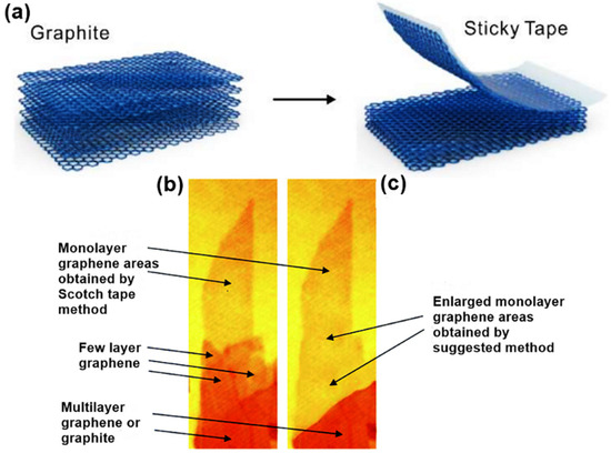
Figure 1. (a) Schematic illustration of the mechanical exfoliation of monolayer grapheme[35]. Optical images of monolayer graphene (b) as-prepared by scotch tape method and (c) as enlarged using Shmavonyan suggested method. Reproduced with permission from[32]. Copyright 2013 National Academy of Sciences of Armenia.
3.2. Liquid-Phase Exfoliation (LPE)
In 2008, Coleman and co-workers used the Liquid-Phase Exfoliation (LPE) technique to synthesize 2D materials[36]. LPE technique involves three steps; first is the dispersion of the bulk materials in a solvent via ultrasonication, secondly is the exfoliation process and thirdly the purification step. The purification step removes the exfoliated flakes from the unexfoliated flakes. To achieve efficient exfoliation using the LPE method, solvents with matching surface energy to the layered bulk crystals are needed; therefore, it becomes challenging getting suitable solvent for each system for each layered bulk crystal. Coleman et al. suggested that the preferred solvents are those that reduced the energy of exfoliation like N-methyl-pyrrolidone (NMP) and isopropanol (IPA)[37]. The Sonication-assisted LPE method is one of the most widely used methods to produce solution-dispersed 2D materials. By controlling the time of sonication, solvent, temperature, power of ultrasonic, surfactants and other additives, one can roughly tune the thickness, concentration and lateral size of the obtained 2D materials. Notwithstanding, there are significant disadvantages of this technique; the production of single-layer nanosheets is low, the size of the nanosheets is relatively small and for the sonication in aqueous polymer and/or surfactant solution, the available surfactants remaining on the exfoliated nanosheets are not suitable for their applications in optoelectronics and energy storage systems. Besides, the sonication process may impact defects on the nanosheets, which will eventually affect their properties[26].
3.3. Chemical Vapor Deposition (CVD)
Generally, the chemical vapor deposition (CVD) method is believed to be the most promising method for large-scale synthesis of high-quality mono- or few-layer 2D materials. In the CVD process for graphene synthesis, carbonaceous gaseous species react in the presence of metal thin films or foils at high temperatures (900–1100 °C) resulting in the decomposition of the carbon species and the formation of the graphene lattice as illustrated in Figure 2. The growth of the graphene on a metal catalyst is determined by several factors, which include the precursor, carbon solubility limit of the metal, lattice parameters, crystal structure, pressure and temperature of the system[38][39]. By adjusting these conditions, the controlled growth of the graphene with a tunable number of layers, crystallinity and lateral size can be obtained[40]. Somani et al. reported the synthesis of planer few-layer graphene (PFLG) by thermal CVD method[41]. They grew the PFLG using low-cost camphor on a nickel substrate. In 2009, Xuesong and co-workers used the CVD technique at 1000 °C to grow large-area high-quality single-layer graphene films using a mixture of methane and hydrogen gas as the carbon precursor on a copper foil substrate[42]. Methane, acetylene and ethylene are the common gaseous carbon precursors used in synthesizing graphene. Among them, methane is known to be the most effective carbon source for graphene synthesis.
Ethylene has also been widely employed besides methane because the relatively high reactivity of ethylene decreases the temperature required for graphene growth using the CVD process. Researchers have also tried several other metals besides Ni, such as Cu, Ir, Ru, Co, Pt, Pd and Re, which have different carbon solubility and catalytic effects. High-quality single-layer graphene grown on polycrystalline Cu films has drawn a lot of interest because it has an advantage of proper control of graphene layers, transferability and low cost[40]. The CVD method has also been employed in the production of large-scale 2D TMDC nanosheets, including alloyed 2D TMDC[26]. Zhan et al. were among the first to show the growth of MoS2 on Si/SiO2 substrate[43]. This was achieved by the deposition of Mo thin film on the Si/SiO2 substrate, followed by the CVD process. The Mo-coated substrate and sulfur powder were kept in a CVD furnace in an inert environment under a constant flow of Nitrogen gas. The temperature was increased to 750 °C and stayed for 90 min, giving time for Mo to react with evaporated sulfur, resulting in the growth of single/few layers MoS2 on Si/SiO2 substrate[26][43].
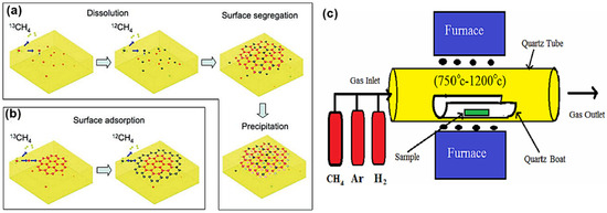
Figure 2. (a,b) Schematic demonstration of the growth mechanism of graphene. Reproduced with permission from[44]. Copyright 2009 American Chemical Society. (c) Schematic illustration of the CVD process setup. Reproduced with permission from[45]. Copyright 2015 CSIR-NISCAIR.
References
- Late, D.J.; Bhat, A.; Rout, C.S. Chapter 2—Fundamentals and Properties of 2D Materials in General and Sensing Applications. In Fundamentals and Sensing Applications of 2D Materials; Hywel, M., Rout, C.S., Late, D.J., Eds.; Woodhead Publishing: Sawston/Cambridge, UK, 2019; pp. 5–24.
- Geim, A.K.; Novoselov, K.S. Nanoscience and Technology: A Collection of Reviews from Nature Journals; Rogers, P., Ed.; World Scientific: Singapore, 2010; p. 11.
- Gianluca Fiori; Francesco Bonaccorso; Giuseppe Iannaccone; Tomás Palacios; Daniel Neumaier; Alan Seabaugh; Sanjay K. Banerjee; Luigi Colombo; Erratum: Electronics based on two-dimensional materials. Nature Nanotechnology 2014, 9, 1063-1063, 10.1038/nnano.2014.283.
- Choi, J.S.; Kim, J.-S.; Byun, I.-S.; Lee, D.H.; Lee, M.J.; Park, B.H.; Lee, C.; Yoon, D.; Cheong, H.; Lee, K.H.; et al. Friction Anisotropy–Driven Domain Imaging on Exfoliated Monolayer Graphene. Science 2011, 333, 607–610.
- Filleter, T.; McChesney, J.L.; Bostwick, A.; Rotenberg, E.; Emtsev, K.V.; Seyller, T.; Horn, K.; Bennewitz, R. Friction and Dissipation in Epitaxial Graphene Films. Phys. Rev. Lett. 2009, 102, 086102.
- Zhang, S.; Ma, T.; Erdemir, A.; Li, Q. Tribology of two-dimensional materials: From mechanisms to modulating strategies. Mater. Today 2019, 26, 67–86.
- Li, S.; Li, Q.; Carpick, R.W.; Gumbsch, P.; Liu, X.Z.; Ding, X.; Sun, J.; Li, J. The evolving quality of frictional contact with grapheme. Nature 2016, 539, 541–545.
- Beatriz Mendoza-Sánchez; Yury Gogotsi; Synthesis of Two-Dimensional Materials for Capacitive Energy Storage. Advanced Materials 2016, 28, 6104-6135, 10.1002/adma.201506133.
- Timmerman, M.A.; Xia, R.; Le, P.T.P.; Wang, Y.; ten Elshof, J.E. Metal Oxide Nanosheets as 2D Building Blocks for the Design of Novel Materials. Chem.-A Eur. J. 2020, 26, 9084–9098.
- Zhang, X.; Xie, Y. Recent advances in free-standing two-dimensional crystals with atomic thickness: Design, assembly and transfer strategies. Chem. Soc. Rev. 2013, 42, 8187–8199.
- Koren, E.; Lörtscher, E.; Rawlings, C.; Knoll, A.W.; Duerig, U. Adhesion and friction in mesoscopic graphite contacts. Science 2015, 348, 679–683.
- Liechti, K.M. Understanding friction in layered materials. Science 2015, 348, 632–633.
- Shinjo, K.; Hirano, M. Dynamics of friction: Superlubric State. Surf. Sci. 1993, 283, 473–478.
- Ky, D.L.C.; Bien-Cuong Tran, K.; Le, C.T.; Kim, Y.S.; Chung, K.-H. Friction characteristics of mechanically exfoliated and CVD-grown single-layer MoS2. Friction 2018, 6, 395–406.
- Changgu Lee; Qunyang Li; William Kalb; Xin-Zhou Liu; Helmuth Berger; Robert W. Carpick; James Hone; Frictional Characteristics of Atomically Thin Sheets. Science 2010, 328, 76-80, 10.1126/science.1184167.
- Kenneth R. Shull; Contact mechanics and the adhesion of soft solids. Materials Science and Engineering: R: Reports 2002, 36, 1-45, 10.1016/s0927-796x(01)00039-0.
- Xiang Zhou; Yuanshuang Liu; Xiangmin Hu; Liang Fang; Yiming Song; Dameng Liu; Jianbin Luo; Influence of elastic property on the friction between atomic force microscope tips and 2D materials. Nanotechnology 2020, 31, 285710, 10.1088/1361-6528/ab7f7d.
- Park, J.Y.; Ogletree, D.F.; Thiel, P.A.; Salmeron, M. Electronic Control of Friction in Silicon pn Junctions. Science 2006, 313, 186.
- Qi, Y.; Park, J.Y.; Hendriksen, B.L.M.; Ogletree, D.F.; Salmeron, M. Electronic contribution to friction on GaAs: An atomic force microscope study. Phys. Rev. B 2008, 77, 184105.
- Berman, D.; Erdemir, A.; Sumant, A.V. Graphene: A new emerging lubricant. Mater. Today 2014, 17, 31–42.
- Hilton, M.R.; Bauer, R.; Didziulis, S.V.; Dugger, M.T.; Keem, J.M.; Scholhamer, J. Structural and tribological studies of MoS2 solid lubricant films having tailored metal-multilayer nanostructures. Surf. Coat. Technol. 1992, 53, 13–23.
- Huaping Xiao; Shuhai Liu; 2D nanomaterials as lubricant additive: A review. Materials & Design 2017, 135, 319-332, 10.1016/j.matdes.2017.09.029.
- Monica Ratoi; Vlad Bogdan Niste; John Walker; Jurgita Zekonyte; Mechanism of Action of WS2 Lubricant Nanoadditives in High-Pressure Contacts. Tribology Letters 2013, 52, 81-91, 10.1007/s11249-013-0195-x.
- Shi, Q.; Tang, H.; Zhu, H.; Tang, G.; Zhang, K.; Zhang, H.; Li, C.; Synthesis and tribological properties of ti-doped NbSe2 nanoparticles. Chalcogenide Lett. 2014, 11, 199–207.
- A. K. Geim; K. S. Novoselov; The rise of graphene. Nat. Mater. 2007, 6, 183–191.
- Parvez, K. Chapter 1—Two-Dimensional Nanomaterials: Crystal Structure and Synthesis. In Biomedical Applications of Graphene and 2D Nanomaterials; Nurunnabi, M., McCarthy, J.R., Eds.; Elsevier: Amsterdam, The Netherlands, 2019; pp. 1–25.
- Yi, M.; Shen, Z. A review on mechanical exfoliation for the scalable production of graphene. J. Mater. Chem. A 2015, 3, 11700–11715
- Novoselov, K.S.; Jiang, D.; Schedin, F.; Booth, T.J.; Khotkevich, V.V.; Morozov, S.V.; Geim, A.K. Two-dimensional atomic crystals. Proc. Natl. Acad. Sci. USA 2005, 102, 10451–10453.
- Li, H.; Wu, J.; Yin, Z.; Zhang, H. Preparation and Applications of Mechanically Exfoliated Single-Layer and Multilayer MoS2 and WSe2 Nanosheets. Acc. Chem. Res. 2014, 47, 1067–1075.
- Li, H.; Lu, G.; Wang, Y.; Yin, Z.; Cong, C.; He, Q.; Wang, L.; Ding, F.; Yu, T.; Zhang, H. Mechanical Exfoliation and Characterization of Single- and Few-Layer Nanosheets of WSe2, TaS2, and TaSe2. Small 2013, 9, 1974–1981.
- Late, D.J.; Doneux, T.; Bougouma, M. Single-layer MoSe2 based NH3 gas sensor. Appl. Phys. Lett. 2014, 105, 233103.
- Shmavonyan, G.S.; Sevoyan, G.; Aroutiounian, V.M.; Enlarging the surface area of monolayer graphene synthesized by mechanical exfoliation. Armen. J. Phys. 2013, 6, 1–6.
- Yitian Peng; Zhuoqiong Wang; Kun Zou; Friction and Wear Properties of Different Types of Graphene Nanosheets as Effective Solid Lubricants. Langmuir 2015, 31, 7782-7791, 10.1021/acs.langmuir.5b00422.
- Yuanbo Zhang; Joshua P. Small; William V. Pontius; Philip Kim; Fabrication and electric-field-dependent transport measurements of mesoscopic graphite devices. Applied Physics Letters 2005, 86, 073104, 10.1063/1.1862334.
- Jin-Ho Lee; Soo-Jeong Park; Jeong-Woo Choi; Electrical Property of Graphene and Its Application to Electrochemical Biosensing. Nanomaterials 2019, 9, 297, 10.3390/nano9020297.
- Yenny Hernandez; Valeria Nicolosi; Mustafa Lotya; Fiona M. Blighe; Zhenyu Sun; Sukanta De; I. T. McGovern; Brendan Holland; Michele Byrne; Yurii K Gun’Ko; et al.John J. BolandPeter NirajGeorg S. DuesbergSatheesh KrishnamurthyRobbie GoodhueJohn HutchisonVittorio ScardaciAndrea C. FerrariJonathan N. Coleman High-yield production of graphene by liquid-phase exfoliation of graphite. Nature Nanotechnology 2008, 3, 563-568, 10.1038/nnano.2008.215.
- Jonathan N. Coleman; Mustafa Lotya; Arlene O’Neill; Shane D. Bergin; Paul J. King; Umar Khan; Karen Young; Alexandre Gaucher; Sukanta De; Ronan J. Smith; et al.I. V. ShvetsSunil K. AroraGeorge StantonHyeyoung KimKangho LeeGyu Tae KimGeorg S. DuesbergToby HallamJohn J. BolandJingjing WangJohn F. DoneganJaime C. GrunlanGregory MoriartyAleksey ShmeliovRebecca J. NichollsJames M. PerkinsEleanor M. GrievesonKoenraad TheuwissenD.W. McCombPeter D. NellistValeria Nicolosi Two-Dimensional Nanosheets Produced by Liquid Exfoliation of Layered Materials. Science 2011, 331, 568-571, 10.1126/science.1194975.
- Oleksiy V. Penkov; Hae-Jin Kim; Hyun-Joon Kim; Dae-Eun Kim; Tribology of graphene: A review. International Journal of Precision Engineering and Manufacturing 2014, 15, 577-585, 10.1007/s12541-014-0373-2.
- Virendra Singh; Daeha Joung; Lei Zhai; Soumen Das; Saiful I. Khondaker; Sudipta Seal; Graphene based materials: Past, present and future. Progress in Materials Science 2011, 56, 1178-1271, 10.1016/j.pmatsci.2011.03.003.
- Yi Zhang; Luyao Zhang; Chongwu Zhou; Review of Chemical Vapor Deposition of Graphene and Related Applications. Accounts of Chemical Research 2013, 46, 2329-2339, 10.1021/ar300203n.
- Prakash R. Somani; Savita P. Somani; Masayoshi Umeno; Planer nano-graphenes from camphor by CVD. Chemical Physics Letters 2006, 430, 56-59, 10.1016/j.cplett.2006.06.081.
- Xuesong Li; Weiwei Cai; Jinho An; Seyoung Kim; Junghyo Nah; Dongxing Yang; Richard Piner; Aruna Velamakanni; Inhwa Jung; Emanuel Tutuc; et al.Sanjay K. BanerjeeLuigi ColomboRodney S. Ruoff Large-Area Synthesis of High-Quality and Uniform Graphene Films on Copper Foils. Science 2009, 324, 1312-1314, 10.1126/science.1171245.
- Yongjie Zhan; Zheng Liu; Sina Najmaei; Pulickel M. Ajayan; Jun Lou; Large-Area Vapor-Phase Growth and Characterization of MoS2Atomic Layers on a SiO2Substrate. Small 2012, 8, 966-971, 10.1002/smll.201102654.
- Xuesong Li; Weiwei Cai; Luigi Colombo; Rodney S. Ruoff; Evolution of Graphene Growth on Ni and Cu by Carbon Isotope Labeling. Nano Letters 2009, 9, 4268-4272, 10.1021/nl902515k.
- Singh, R.; Kumar, D.; Tripathi, C.C.; Graphene: Potential material for nanoelectronics applications. J. Pure Appl. Phys. 2015, 53, 501–513.

