+1 credit
| Version | Summary | Created by | Modification | Content Size | Created at | Operation |
|---|---|---|---|---|---|---|
| 1 | Melvin M. Mashingaidze | -- | 3766 | 2022-04-11 18:58:18 | | | |
| 2 | Peter Tang | Meta information modification | 3766 | 2022-04-12 02:57:59 | | |
Video Upload Options
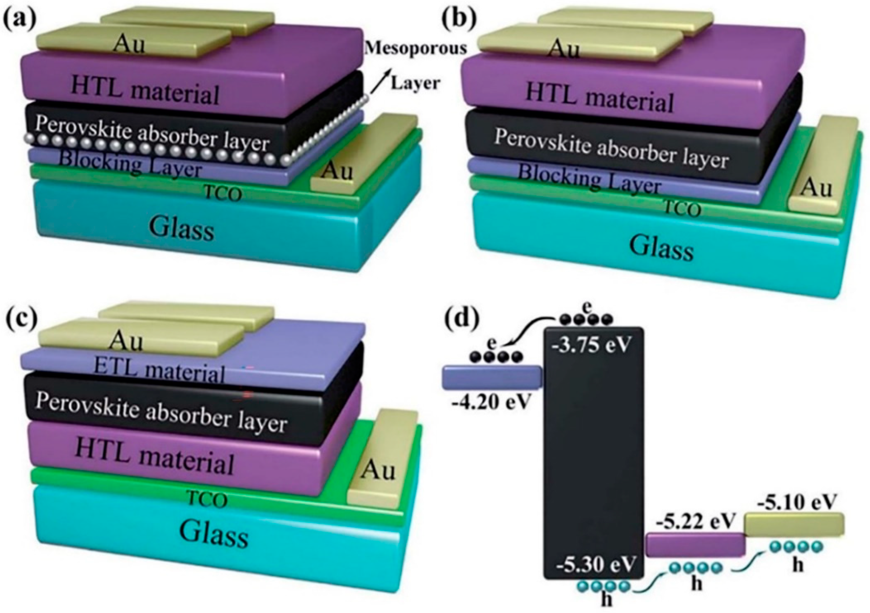
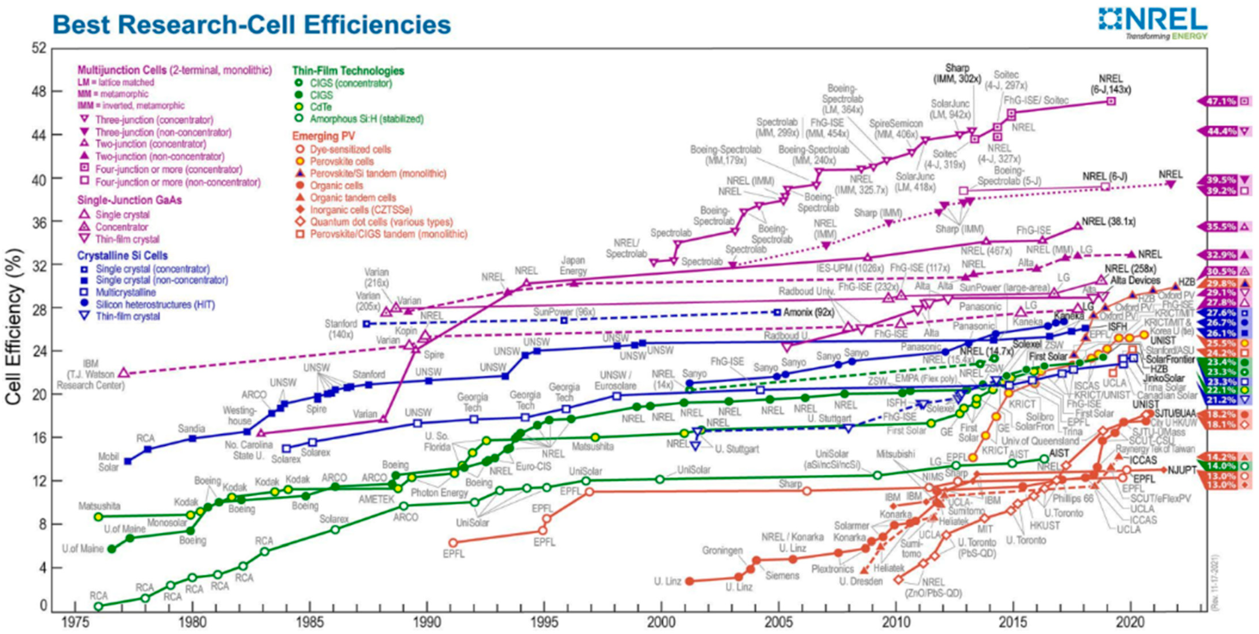
Solar energy is one of the most encouraging, abundant, green, and renewable sources for decreasing or even replacing traditional energy in the future. The energy provided by the sun in one hour is sufficient to supply the Earth’s needs for an entire year. The recent rapid development in perovskite solar cells (PSCs) has led to significant research interest due to their notable photovoltaic performance, currently exceeding 25% power conversion efficiency for small-area PSCs. The materials used to fabricate PSCs dominate the current photovoltaic market, especially with the rapid increase in efficiency and performance.
1. Introduction
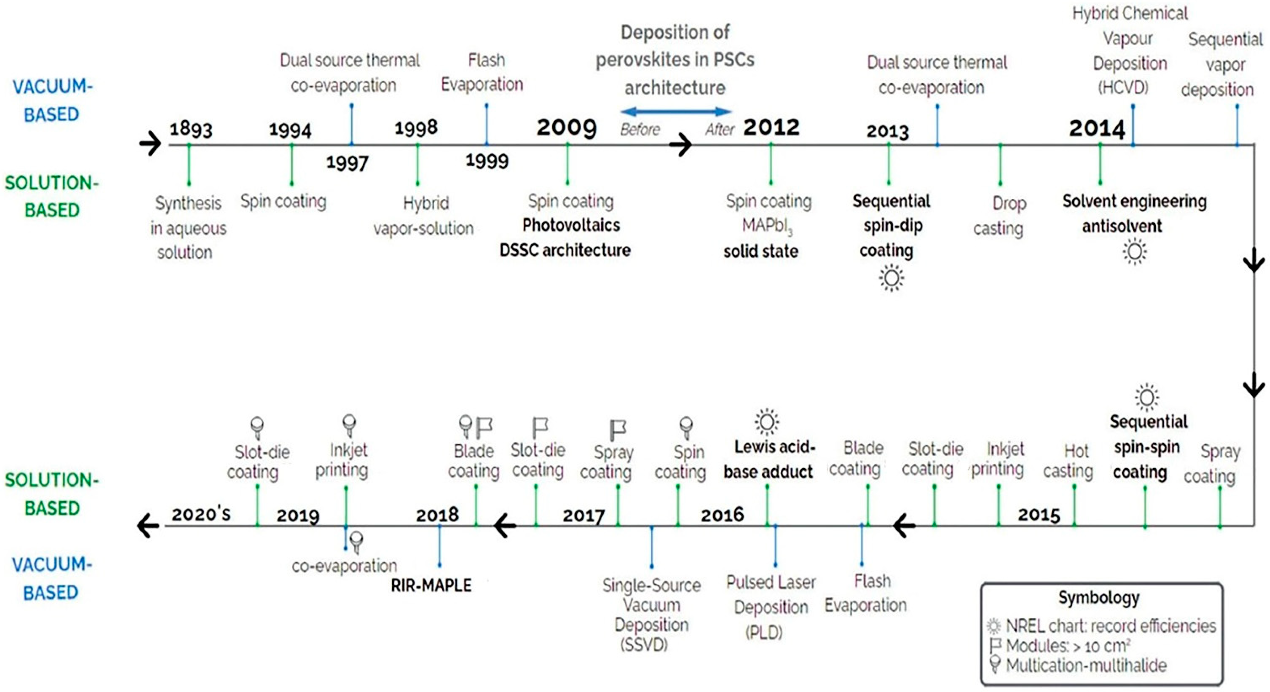
2. Large-Area PSC Preparation Methods and Fabrication Technologies
|
Solution Processing Method |
Vapor Deposition Method |
|---|---|
|
Spray coating |
Vacuum thermal evaporation |
|
Ink-jet printing |
Co-evaporation |
|
Spin coating |
Sequential evaporation |
|
Slot-die coating |
Flash evaporation |
|
Blade coating/Knife-over edge coating |
Vapor assisted solution process |
|
Vacuum flash-assisted solution process |
Chemical vapor deposition |
- In recent years, vacuum thermal evaporation has lost its position as the fabrication method of choice.
- Spray coating and blade coating have also seen a reduction in use by PSC researchers.
- PSC researchers have increasingly adopted ink-jet printing and slot-die coating.
- PSC researchers are working on overcoming the technological impediments to the synthesis and commercialization of large-area PSCs.
- Not all perovskite thin-film fabrication technologies have been used to create large-area solar cells despite some methods such as thermal evaporation having significant scalability potential.
- In recent publications, the slot-die coating has demonstrated the highest PCE for large-area PSCs, implying that it has a high potential for ushering in PSC commercialization.
2.1. Spin Coating
2.2. Spray Coating Methods: Spray Printing, Spray Deposition, Spray Pyrolysis, and Ultrasonic Spray
2.3. Slot-Die Coating Method
2.4. Blade-Coating Method
2.5. Ink-Jet Printing Method
2.6. Vacuum Flash-Assisted Solution Method
2.7. Chemical Vapor Deposition Method
2.8. Sequential Evaporation Method
2.9. Co-Evaporation Method
2.10. Flash Evaporation Method
2.11. Vacuum Thermal Evaporation Method
2.12. Multi-Flow Air Knife Method
References
- Kour, R.; Arya, S.; Verma, S.; Gupta, J.; Bandhoria, P.; Bharti, V.; Datt, R.; Gupta, V. Potential Substitutes for Replacement of Lead in Perovskite Solar Cells: A Review. Glob. Chall. 2019, 3, 1900050.
- Rajagopal, A.; Yao, K.; Jen, A.K.Y. Toward Perovskite Solar Cell Commercialization: A Perspective and Research Roadmap Based on Interfacial Engineering. Adv. Mater. 2018, 30, 1800455.
- Enriquez, C.; Hodges, D.; De La Rosa, A.; Valerio Frias, L.; Ramirez, Y.; Rodriguez, V.; Rivera, D.; Telle, A. Perovskite Solar Cells. In Proceedings of the 2019 IEEE 46th Photovoltaic Specialists Conference (PVSC), Chicago, IL, USA, 16–21 June 2019.
- Hamukwaya, S.L.; Zhao, Z.; Wang, N.; Liu, H.; Umar, A.; Zhang, J.; Wu, T.; Guo, Z. Enhanced Photocatalytic Activity of B, N-Codoped TiO2 by a New Molten Nitrate Process. J. Nanosci. Nanotechnol. 2018, 19, 839–849.
- Lewis, N.S.; Nocera, D.G. Powering the planet: Chemical challenges in solar energy utilization. Proc. Natl. Acad. Sci. USA 2006, 103, 15729–15735.
- Wang, R.; Mujahid, M.; Duan, Y.; Wang, Z.K.; Xue, J.; Yang, Y. A Review of Perovskites Solar Cell Stability. Adv. Funct. Mater. 2019, 29, 1808843.
- Li, D.; Shi, J.; Xu, Y.; Luo, Y.; Wu, H.; Meng, Q. Inorganic-organic halide perovskites for new photovoltaic technology. Natl. Sci. Rev. 2018, 5, 559–576.
- Niu, G.; Guo, X.; Wang, L. Review of recent progress in chemical stability of perovskite solar cells. J. Mater. Chem. A 2015, 3, 8970–8980.
- Parisi, M.L.; Maranghi, S.; Basosi, R. The evolution of the dye sensitized solar cells from Grätzel prototype to up-scaled solar applications: A life cycle assessment approach. Renew. Sustain. Energy Rev. 2014, 39, 124–138.
- Uddin, A.; Upama, M.B.; Yi, H.; Duan, L. Encapsulation of organic and perovskite solar cells: A review. Coatings 2019, 9, 65.
- Tang, H.; He, S.; Peng, C. A Short Progress Report on High-Efficiency Perovskite Solar Cells. Nanoscale Res. Lett. 2017, 12, 410.
- Wang, F.; Cao, Y.; Chen, C.; Chen, Q.; Wu, X.; Li, X.; Qin, T.; Huang, W. Materials toward the Upscaling of Perovskite Solar Cells: Progress, Challenges, and Strategies. Adv. Funct. Mater. 2018, 28, 1803753.
- Pitchaiya, S.; Natarajan, M.; Santhanam, A.; Asokan, V.; Yuvapragasam, A.; Madurai Ramakrishnan, V.; Palanisamy, S.E.; Sundaram, S.; Velauthapillai, D. A review on the classification of organic/inorganic/carbonaceous hole transporting materials for perovskite solar cell application. Arab. J. Chem. 2020, 13, 2526–2557.
- Assadi, M.K.; Bakhoda, S.; Saidur, R.; Hanaei, H. Recent progress in perovskite solar cells. Renew. Sustain. Energy Rev. 2018, 81, 2812–2822.
- Chen, Y.; Zhang, L.; Zhang, Y.; Gao, H.; Yan, H. Large-area perovskite solar cells-a review of recent progress and issues. RSC Adv. 2018, 8, 10489–10508.
- Zhao, Y.; Ma, F.; Gao, F.; Yin, Z.; Zhang, X.-W.; You, J. Research Progresses in Large-Area Perovskite Solar Cells. Photonics Res. 2020, 8, A1–A15.
- Li, X.; Bi, D.; Yi, C.; Décoppet, J.D.; Luo, J.; Zakeeruddin, S.M.; Hagfeldt, A.; Grätzel, M. A vacuum flash-assisted solution process for high-efficiency large-area perovskite solar cells. Science 2016, 353, 58–62.
- Lee, J.W.; Lee, D.K.; Jeong, D.N.; Park, N.G. Control of Crystal Growth toward Scalable Fabrication of Perovskite Solar Cells. Adv. Funct. Mater. 2019, 29, 1807047.
- Kim, D.H.; Whitaker, J.B.; Li, Z.; van Hest, M.F.A.M.; Zhu, K. Outlook and Challenges of Perovskite Solar Cells toward Terawatt-Scale Photovoltaic Module Technology. Joule 2018, 2, 1437–1451.
- Park, N.G. Research Direction toward Scalable, Stable, and High Efficiency Perovskite Solar Cells. Adv. Energy Mater. 2020, 10, 1903106.
- Dai, X.; Xu, K.; Wei, F. Recent progress in perovskite solar cells: The perovskite layer. Beilstein J. Nanotechnol. 2020, 11, 51–60.
- Kim, J.; Yun, J.S.; Cho, Y.; Lee, D.S.; Wilkinson, B.; Soufiani, A.M.; Deng, X.; Zheng, J.; Shi, A.; Lim, S.; et al. Overcoming the Challenges of Large-Area High-Efficiency Perovskite Solar Cells. ACS Energy Lett. 2017, 2, 1978–1984.
- Park, N.G.; Zhu, K. Scalable fabrication and coating methods for perovskite solar cells and solar modules. Nat. Rev. Mater. 2020, 5, 333–350.
- Gao, F.; Zhao, Y.; Zhang, X.; You, J. Recent Progresses on Defect Passivation toward Efficient Perovskite Solar Cells. Adv. Energy Mater. 2020, 10, 1902650.
- Dai, T.; Cao, Q.; Yang, L.; Aldamasy, M.H.; Li, M.; Liang, Q.; Lu, H.; Dong, Y.; Yang, Y. Strategies for High-Performance Large-Area Perovskite Solar Cells toward Commercialization. Crystals 2021, 11, 295.
- Niu, T.; Zhu, W.; Zhang, Y.; Xue, Q.; Jiao, X.; Wang, Z.; Xie, Y.M.; Li, P.; Chen, R.; Huang, F.; et al. D-A-π-A-D-type Dopant-free Hole Transport Material for Low-Cost, Efficient, and Stable Perovskite Solar Cells. Joule 2021, 5, 249–269.
- Li, Z.; Klein, T.R.; Kim, D.H.; Yang, M.; Berry, J.J.; Van Hest, M.F.A.M.; Zhu, K. Scalable fabrication of perovskite solar cells. Nat. Rev. Mater. 2018, 3, 18017.
- Bae, I.G.; Park, B. All-self-metered solution-coating process in ambient air for the fabrication of efficient, large-area, and semitransparent perovskite solar cells. Sustain. Energy Fuels 2020, 4, 3115–3128.
- Burschka, J.; Pellet, N.; Moon, S.J.; Humphry-Baker, R.; Gao, P.; Nazeeruddin, M.K.; Grätze, M. Sequential deposition as a route to high-performance perovskite-sensitized solar cells. Nature 2013, 499, 316–319.
- Xiao, Z.; Bi, C.; Shao, Y.; Dong, Q.; Wang, Q.; Yuan, Y.; Wang, C.; Gao, Y.; Huang, J. Efficient, high yield perovskite photovoltaic devices grown by interdiffusion of solution-processed precursor stacking layers. Energy Environ. Sci. 2014, 7, 2619–2623.
- Liu, X.; Cao, L.; Guo, Z.; Li, Y.; Gao, W.; Zhou, L. A review of perovskite photovoltaic materials’ synthesis and applications via chemical vapor deposition method. Materials 2019, 12, 3304.
- Shalan, A.E. Challenges and approaches towards upscaling the assembly of hybrid perovskite solar cells. Mater. Adv. 2020, 1, 292–309.
- Hwang, K.; Jung, Y.S.; Heo, Y.J.; Scholes, F.H.; Watkins, S.E.; Subbiah, J.; Jones, D.J.; Kim, D.Y.; Vak, D. Toward large scale roll-to-roll production of fully printed perovskite solar cells. Adv. Mater. 2015, 27, 1241–1247.
- Razza, S.; Di Giacomo, F.; Matteocci, F.; Cinà, L.; Palma, A.L.; Casaluci, S.; Cameron, P.; Epifanio, A.D.; Licoccia, S.; Reale, A.; et al. Perovskite solar cells and large area modules (100 cm2) based on an air flow-assisted PbI2 blade coating deposition process. J. Power Sources 2015, 277, 286–291.
- NREL. Best-Research-Cell-Efficiencies-Rev211117. Available online: https://www.nrel.gov/pv/assets/pdfs/best-research-cell-efficiencies-rev211117.pdf (accessed on 22 January 2022).
- Zhihui Photovolt. The Efficiency of Perovskite Components Exceeds 18%, and There Is Huge Room for Imagination in the Future! 2020. Available online: Http://solar.in-en.com/html/solar-2352538.shtml (accessed on 18 January 2022).
- Jean, J.; Xiao, J.; Nick, R.; Moody, N.; Nasilowski, M.; Bawendi, M.; Bulović, V. Synthesis cost dictates the commercial viability of lead sulfide and perovskite quantum dot photovoltaics. Energy Environ. Sci. 2018, 11, 2295–2305.
- Song, Z.; McElvany, C.L.; Phillips, A.B.; Celik, I.; Krantz, P.W.; Watthage, S.C.; Liyanage, G.K.; Apul, D.; Heben, M.J. A technoeconomic analysis of perovskite solar module manufacturing with low-cost materials and techniques. Energy Environ. Sci. 2017, 10, 1297–1305.
- Zhang, Q.; Hao, F.; Li, J.; Zhou, Y.; Wei, Y.; Lin, H. Perovskite solar cells: Must lead be replaced-and can it be done? Sci. Technol. Adv. Mater. 2018, 19, 425–442.
- Swartwout, R.; Hoerantner, M.T.; Bulović, V. Scalable Deposition Methods for Large-Area Production of Perovskite Thin Films. Energy Environ. Mater. 2019, 2, 119–145.
- Yang, Z.; Zhang, S.; Li, L.; Chen, W. Research progress on large-area perovskite thin films and solar modules. J. Mater. 2017, 3, 231–244.
- Soto-Montero, T.; Soltanpoor, W.; Morales-Masis, M. Pressing challenges of halide perovskite thin film growth. APL Mater. 2020, 8, 110903.
- Borchert, J.; Milot, R.L.; Patel, J.B.; Davies, C.L.; Wright, A.D.; Martínez Maestro, L.; Snaith, H.J.; Herz, L.M.; Johnston, M.B. Large-Area, Highly Uniform Evaporated Formamidinium Lead Triiodide Thin Films for Solar Cells. ACS Energy Lett. 2017, 2, 2799–2804.
- Malinkiewicz, O.; Yella, A.; Lee, Y.H.; Espallargas, G.M.; Graetzel, M.; Nazeeruddin, M.K.; Bolink, H.J. Perovskite solar cells employing organic charge-transport layers. Nat. Photon. 2014, 8, 128–132.
- Larson, R.G.; Rehg, T.J. Spin Coating. In Liquid Film Coating; Chapman & Hall: Glasgow, UK, 1997.
- Tzounis, L.; Stergiopoulos, T.; Zachariadis, A.; Gravalidis, C.; Laskarakis, A.; Logothetidis, S. Perovskite solar cells from small scale spin coating process towards roll-to-roll printing: Optical and Morphological studies. Mater. Today Proc. 2017, 4, 5082–5089.
- Kim, M.K.; Lee, H.S.; Pae, S.R.; Kim, D.J.; Lee, J.Y.; Gereige, I.; Park, S.; Shin, B. Effects of temperature and coating speed on the morphology of solution-sheared halide perovskite thin-films. J. Mater. Chem. A 2018, 6, 24911–24919.
- Han, G.S.; Kim, J.; Bae, S.; Han, S.; Kim, Y.J.; Gong, O.Y.; Lee, P.; Ko, M.J.; Jung, H.S. Spin-Coating Process for 10 cm × 10 cm Perovskite Solar Modules Enabled by Self-Assembly of SnO2 Nanocolloids. ACS Energy Lett. 2019, 4, 1845–1851.
- Barrows, A.T.; Pearson, A.J.; Kwak, C.K.; Dunbar, A.D.F.; Buckley, A.R.; Lidzey, D.G. Efficient planar heterojunction mixed-halide perovskite solar cells deposited via spray-deposition. Energy Environ. Sci. 2014, 7, 2944–2950.
- Tait, J.G.; Manghooli, S.; Qiu, W.; Rakocevic, L.; Kootstra, L.; Jaysankar, M.; Masse De La Huerta, C.A.; Paetzold, U.W.; Gehlhaar, R.; Cheyns, D.; et al. Rapid composition screening for perovskite photovoltaics via concurrently pumped ultrasonic spray coating. J. Mater. Chem. A 2016, 4, 3792–3797.
- Das, S.; Yang, B.; Gu, G.; Joshi, P.C.; Ivanov, I.N.; Rouleau, C.M.; Aytug, T.; Geohegan, D.B.; Xiao, K. High-Performance Flexible Perovskite Solar Cells by Using a Combination of Ultrasonic Spray-Coating and Low Thermal Budget Photonic Curing. ACS Photonics 2015, 2, 680–686.
- Yao, J.; Yang, L.; Cai, F.; Yan, Y.; Gurney, R.S.; Liu, D.; Wang, T. The impacts of PbI2 purity on the morphology and device performance of one-step spray-coated planar heterojunction perovskite solar cells. Sustain. Energy Fuels 2018, 2, 436–443.
- Kim, H.S.; Im, S.H.; Park, N.G. Organolead halide perovskite: New horizons in solar cell research. J. Phys. Chem. C 2014, 118, 5615–5625.
- Siansonic. Ultrasonic and Piezoelectric Technologies. 2020. Available online: Https://www.Siansonic.Com/Products (accessed on 22 January 2022).
- Sono-Tek. Ultrasonic System. Available online: http://www.siansonic.com/ (accessed on 22 January 2022).
- Gamliel, S.; Dymshits, A.; Aharon, S.; Terkieltaub, E.; Etgar, L. Micrometer Sized Perovskite Crystals in Planar Hole Conductor Free Solar Cells. J. Phys. Chem. C 2015, 119, 19722–19728.
- Huang, H.; Shi, J.; Zhu, L.; Li, D.; Luo, Y.; Meng, Q. Two-step ultrasonic spray deposition of CH3NH3PbI3 for efficient and large-area perovskite solar cell. Nano Energy 2016, 27, 352–358.
- Remeika, M.; Raga, S.R.; Zhang, S.; Qi, Y. Transferrable optimization of spray-coated PbI2 films for perovskite solar cell fabrication. J. Mater. Chem. A 2017, 5, 5709–5718.
- Chai, G.; Luo, S.; Zhou, H.; Daoud, W.A. CH3NH3PbI3−xBrx perovskite solar cells via spray assisted two-step deposition: Impact of bromide on stability and cell performance. Mater. Des. 2017, 125, 222–229.
- Bishop, J.E.; Mohamad, D.K.; Wong-Stringer, M.; Smith, A.; Lidzey, D.G. Spray-cast multilayer perovskite solar cells with an active-area of 1.5 cm2. Sci. Rep. 2017, 7, 7962.
- Heo, J.H.; Lee, M.H.; Jang, M.H.; Im, S.H. Highly efficient CH3NH3PbI3-xClx mixed halide perovskite solar cells prepared by re-dissolution and crystal grain growth via spray coating. J. Mater. Chem. A 2016, 4, 17636–17642.
- Ye, F.; Chen, H.; Xie, F.; Tang, W.; Yin, M.; He, J.; Bi, E.; Wang, Y.; Yang, X.; Han, L. Soft-cover deposition of scaling-up uniform perovskite thin films for high cost-performance solar cells. Energy Environ. Sci. 2016, 9, 2295–2301.
- Wu, Y.; Yang, X.; Chen, W.; Yue, Y.; Cai, M.; Xie, F.; Bi, E.; Islam, A.; Han, L. Perovskite solar cells with 18.21% efficiency and area over 1 cm2 fabricated by heterojunction engineering. Nat. Energy 2016, 1, 16148.
- Wu, Y.; Xie, F.; Chen, H.; Yang, X.; Su, H.; Cai, M.; Zhou, Z.; Noda, T.; Han, L. Thermally Stable MAPbI3 Perovskite Solar Cells with Efficiency of 19.19% and Area over 1 cm2 achieved by Additive Engineering. Adv. Mater. 2017, 29, 1701073.
- Di Giacomo, F.; Fakharuddin, A.; Jose, R.; Brown, T.M. Progress, challenges and perspectives in flexible perovskite solar cells. Energy Environ. Sci. 2016, 9, 3007–3035.
- Cao, K.; Zuo, Z.; Cui, J.; Shen, Y.; Moehl, T.; Zakeeruddin, S.M.; Grätzel, M.; Wang, M. Efficient screen printed perovskite solar cells based on mesoscopic TiO2/Al2O3/NiO/carbon architecture. Nano Energy 2015, 17, 171–179.
- Li, X.; Yang, J.; Jiang, Q.; Chu, W.; Zhang, D.; Zhou, Z.; Xin, J. Synergistic Effect to High-Performance Perovskite Solar Cells with Reduced Hysteresis and Improved Stability by the Introduction of Na-Treated TiO2 and Spraying-Deposited CuI as Transport Layers. ACS Appl. Mater. Interfaces 2017, 9, 41354–41362.
- Yang, W.S.; Park, B.-W.W.; Jung, E.H.; Jeon, N.J.; Kim, Y.C.; Lee, D.U.; Shin, S.S.; Seo, J.; Kim, E.K.; Noh, J.H.; et al. Iodide management in formamidinium-lead-halide-based perovskite layers for efficient solar cells. Science 2017, 356, 1376–1379.
- Chen, H.; Ye, F.; Tang, W.; He, J.; Yin, M.; Wang, Y.; Xie, F.; Bi, E.; Yang, X.; Grätzel, M.; et al. A solvent-and vacuum-free route to large-area perovskite films for efficient solar modules. Nature 2017, 550, 92–95.
- Lu, J.; Jiang, L.; Li, W.; Li, F.; Pai, N.K.; Scully, A.D.; Tsai, C.M.; Bach, U.; Simonov, A.N.; Cheng, Y.B.; et al. Diammonium and Monoammonium Mixed-Organic-Cation Perovskites for High Performance Solar Cells with Improved Stability. Adv. Energy Mater. 2017, 7, 1700444.
- Jiang, Y.; Leyden, M.R.; Qiu, L.; Wang, S.; Ono, L.K.; Wu, Z.; Juarez-Perez, E.J.; Qi, Y. Combination of Hybrid CVD and Cation Exchange for Upscaling Cs-Substituted Mixed Cation Perovskite Solar Cells with High Efficiency and Stability. Adv. Funct. Mater. 2018, 28, 1703835.
- Matteocci, F.; Cinà, L.; Di Giacomo, F.; Razza, S.; Palma, A.L.; Guidobaldi, A.; D’Epifanio, A.; Licoccia, S.; Brown, T.M.; Reale, A.; et al. High efficiency photovoltaic module based on mesoscopic organometal halide perovskite. Prog. Photovolt. Res. Appl. 2016, 24, 436–445.
- Kim, A.; Lee, H.; Kwon, H.C.; Jung, H.S.; Park, N.G.; Jeong, S.; Moon, J. Fully solution-processed transparent electrodes based on silver nanowire composites for perovskite solar cells. Nanoscale 2016, 8, 6308–6316.
- Khoa, N.H.; Tanaka, Y.; Goh, W.P.; Jiang, C. A solution processed Ag-nanowires/C60 composite top electrode for efficient and translucent perovskite solar cells. Sol. Energy 2020, 196, 582–588.
- Han, K.; Xie, M.; Zhang, L.; Yan, L.; Wei, J.; Ji, G.; Luo, Q.; Lin, J.; Hao, Y.; Ma, C.Q. Fully solution processed semi-transparent perovskite solar cells with spray-coated silver nanowires/ZnO composite top electrode. Sol. Energy Mater. Sol. Cells 2018, 185, 399–405.
- Dou, Y.; Liu, Z.; Wu, Z.; Liu, Y.; Li, J.; Leng, C.; Fang, D.; Liang, G.; Xiao, J.; Li, W.; et al. Self-augmented ion blocking of sandwiched 2D/1D/2D electrode for solution processed high efficiency semitransparent perovskite solar cell. Nano Energy 2020, 71, 104567.
- Habibi, M.; Rahimzadeh, A.; Bennouna, I.; Eslamian, M. Defect-Free Large-Area (25 cm2) Light Absorbing Perovskite Thin Films Made by Spray Coating. Coatings 2017, 7, 42.
- Deng, Y.; Zheng, X.; Bai, Y.; Wang, Q.; Zhao, J.; Huang, J. Surfactant-controlled ink drying enables high-speed deposition of perovskite films for efficient photovoltaic modules. Nat. Energy 2018, 3, 560–566.
- Deng, Y.; Wang, Q.; Yuan, Y.; Huang, J. Vividly colorful hybrid perovskite solar cells by doctor-blade coating with perovskite photonic nanostructures. Mater. Horiz. 2015, 2, 578–583.
- Deng, Y.; Peng, E.; Shao, Y.; Xiao, Z.; Dong, Q.; Huang, J. Scalable fabrication of efficient organolead trihalide perovskite solar cells with doctor-bladed active layers. Energy Environ. Sci. 2015, 8, 1544–1550.
- Li, C.; Yin, J.; Chen, R.; Lv, X.; Feng, X.; Wu, Y.; Cao, J. Monoammonium Porphyrin for Blade-Coating Stable Large-Area Perovskite Solar Cells with >18% Efficiency. J. Am. Chem. Soc. 2019, 141, 6345–6351.
- Wu, W.Q.; Yang, Z.; Rudd, P.N.; Shao, Y.; Dai, X.; Wei, H.; Zhao, J.; Fang, Y.; Wang, Q.; Liu, Y.; et al. Bilateral alkylamine for suppressing charge recombination and improving stability in blade-coated perovskite solar cells. Sci. Adv. 2019, 5, 2001906.
- Lin, Y.; Ye, X.; Wu, Z.; Zhang, C.; Zhang, Y.; Su, H.; Yin, J.; Li, J. Manipulation of the crystallization of perovskite films induced by a rotating magnetic field during blade coating in air. J. Mater. Chem. A 2018, 6, 3986–3995.
- Wu, W.Q.; Wang, Q.; Fang, Y.; Shao, Y.; Tang, S.; Deng, Y.; Lu, H.; Liu, Y.; Li, T.; Yang, Z.; et al. Molecular doping enabled scalable blading of efficient hole-transport-layer-free perovskite solar cells. Nat. Commun. 2018, 9, 1625.
- Kong, W.; Wang, G.; Zheng, J.; Hu, H.; Chen, H.; Li, Y.; Hu, M.; Zhou, X.; Liu, C.; Chandrashekar, B.N.; et al. Fabricating High-Efficient Blade-Coated Perovskite Solar Cells under Ambient Condition Using Lead Acetate Trihydrate. Sol. RRL 2018, 2, 1700214.
- Zhong, Y.; Munir, R.; Li, J.; Tang, M.-C.; Niazi, M.R.; Smilgies, D.-M.; Zhao, K.; Amassian, A. Blade-Coated Hybrid Perovskite Solar Cells with Efficiency > 17%: An In Situ Investigation. ACS Energy Lett. 2018, 3, 1078–1085.
- Yang, Z.; Chueh, C.C.; Zuo, F.; Kim, J.H.; Liang, P.W.; Jen, A.K.Y. High-Performance Fully Printable Perovskite Solar Cells via Blade-Coating Technique under the Ambient Condition. Adv. Energy Mater. 2015, 5, 1500328.
- Li, J.; Munir, R.; Fan, Y.; Niu, T.; Liu, Y.; Zhong, Y.; Yang, Z.; Tian, Y.; Liu, B.; Sun, J.; et al. Phase Transition Control for High-Performance Blade-Coated Perovskite Solar Cells. Joule 2018, 2, 1313–1330.
- Hu, Q.; Wu, H.; Sun, J.; Yan, D.; Gao, Y.; Yang, J. Large-area perovskite nanowire arrays fabricated by large-scale roll-to-roll micro-gravure printing and doctor blading. Nanoscale 2016, 8, 5350–5357.
- Mathies, F.; Abzieher, T.; Hochstuhl, A.; Glaser, K.; Colsmann, A.; Paetzold, U.W.; Hernandez-Sosa, G.; Lemmer, U.; Quintilla, A. Multipass inkjet printed planar methylammonium lead iodide perovskite solar cells. J. Mater. Chem. A 2016, 4, 19207–19213.
- Karunakaran, S.K.; Arumugam, G.M.; Yang, W.; Ge, S.; Khan, S.N.; Lin, X.; Yang, G. Recent progress in inkjet-printed solar cells. J. Mater. Chem. A 2019, 7, 13873–13902.
- Lee, J.W.; Kim, H.S.; Park, N.G. Lewis Acid-Base Adduct Approach for High-Efficiency Perovskite Solar Cells. Acc. Chem. Res. 2016, 49, 311–319.
- Liu, M.; Johnston, M.B.; Snaith, H.J. Efficient planar heterojunction perovskite solar cells by vapor deposition. Nature 2013, 501, 395–398.
- Chen, X.; Cao, H.; Yu, H.; Zhu, H.; Zhou, H.; Yang, L.; Yin, S. Large-area, high-quality organic-inorganic hybrid perovskite thin films: Via a controlled vapor-solid reaction. J. Mater. Chem. A 2016, 4, 9124–9132.
- Hu, H.; Wang, D.; Zhou, Y.; Zhang, J.; Lv, S.; Pang, S.; Chen, X.; Liu, Z.; Padture, N.P.; Cui, G. Vapour-based processing of hole-conductor-free CH3NH3PbI3 perovskite/C60 fullerene planar solar cells. RSC Adv. 2014, 4, 28964–28967.
- Hsiao, S.Y.; Lin, H.L.; Lee, W.H.; Tsai, W.L.; Chiang, K.M.; Liao, W.Y.; Ren-Wu, C.Z.; Chen, C.Y.; Lin, H.W. Efficient All-Vacuum Deposited Perovskite Solar Cells by Controlling Reagent Partial Pressure in High Vacuum. Adv. Mater. 2016, 28, 7013–7019.
- Ávila, J.; Momblona, C.; Boix, P.P.; Sessolo, M.; Bolink, H.J. Vapor-Deposited Perovskites: The Route to High-Performance Solar Cell Production? Joule 2017, 1, 431–442.
- Longo, G.; Gil-Escrig, L.; Degen, M.J.; Sessolo, M.; Bolink, H.J. Perovskite solar cells prepared by flash evaporation. Chem. Commun. 2015, 51, 7376–7378.
- Rong, Y.; Hu, Y.; Mei, A.; Tan, H.; Saidaminov, M.I.; Seok, S., II; McGehee, M.D.; Sargent, E.H.; Han, H. Challenges for commercializing perovskite solar cells. Science 2018, 80, 361.
- Ke, W.; Zhao, D.; Cimaroli, A.J.; Grice, C.R.; Qin, P.; Liu, Q.; Xiong, L.; Yan, Y.; Fang, G. Effects of annealing temperature of tin oxide electron selective layers on the performance of perovskite solar cells. J. Mater. Chem. A 2015, 3, 24163–24168.
- Gao, L.L.; Li, C.X.; Li, C.J.; Yang, G.J. Large-area high-efficiency perovskite solar cells based on perovskite films dried by the multi-flow air knife method in air. J. Mater. Chem. A 2017, 5, 1548–1557.