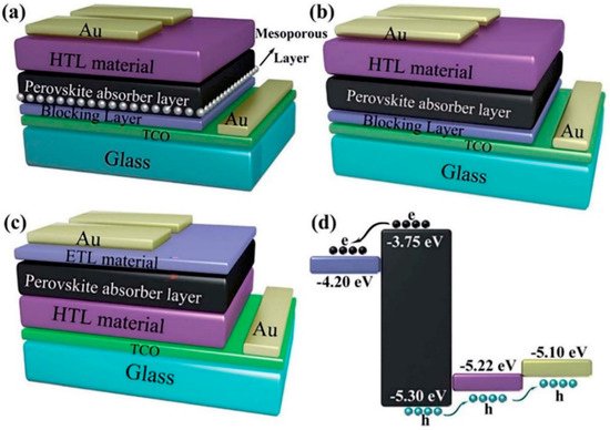
Timeline for application of vacuum deposition methods vs. solution processing methods in the fabrication of inorganic and mixed halide perovskites. The symbology legend defines fabrication methods used; reported National Renewable Energy Laboratory (NREL) record efficiencies, modules, and multi-cation/multi-halide compositions
.
2.1. Spin Coating
Spin coating is a batch method in which a liquid film is spread by centrifugal force onto a rotating substrate
[45]. The method has been extensively used to manufacture small PSCs of about 0.1 cm
2 and large-area devices of 1 cm
2. This method is categorized into one-step and two-step processes. Perovskite devices fabricated through spin coating have reached PCEs of over 9.4%
[46].
Spin coating has potential for the production of moderately large-area PSCs if evaporation of the solvent can be closely regulated
[2][40][2,40], and this has been demonstrated by the authors of
[47], who prepared a large-area perovskite film of 57 cm
2. The two-step sequential processing method provides better performance than the one-step method for perovskite deposition. In addition, film quality can be enhanced through controlled crystal growth and the post-annealing time
[32][48][32,48].
2.2. Spray Coating Methods: Spray Printing, Spray Deposition, Spray Pyrolysis, and Ultrasonic Spray
Spray coating is a low-temperature and low-ink-concentration coating method that is suitable for large-area technology and it is a widely used deposition method in the industry
[16]. It is an easily scalable method for fabricating large-area thin perovskite films. Perovskite film obtained through this method displays high uniformity over large areas.
Spray coating is accomplished through a series of four distinct activities: production of the ink droplets, placement of the droplets on the substrate, amalgamation of the droplets into a wet film, and film drying. Of all the scalable methods, spray coating is the most diverse. It presently encompasses two methods of deposition: one-step and two-step. One-step film deposition solutions comprise aprotic solvents
[16][49][50][51][16,58,59,60]. Two-step methods use metal salts deposited by either spray coating or spin coating in an aprotic solvent lacking an acidic proton and hydroxyl and amine groups
[40][52][40,61].
Spray coating is the fastest process by which a subjected fluid can be automatically driven to exhibit capillary waves and obtain a scalable substrate
[21]. It is based on the atomization of a fluid and the depositing of the atomized fluid droplets onto a suitable surface. Atomization can be generated through various methods: high flow gas, ultrasonic stimulation, or cavitation of the ink itself
[51][53][60,62]. The aforementioned atomization methods are generally scalable.
Ultrasonic spray coaters are the latest technology for efficiently preparing various functional thin films for photovoltaic cells
[54][55][65,66]. Liquid thin-film coating technology has been developed for different applications.
Organic salts are deposited on the substrate by spray coating or immersion in an alcohol solution, using isopropanol as the solvent
[56][57][58][59][67,68,69,70]. The results vary depending on the method of perovskite solution deposition employed. The single-step deposition method has been used in compositions encompassing MAI, lead iodide, and iodide chloride varieties
[56][60][67,71]. The solvents used were DMF, DMSO, gamma-butyrolactone (GBL), DMF-DMSO, and GBL-DMSO; some studies used processing additives such as hydrogen iodide (HI)
[60][71]. The highest reported PCE for perovskite films made through this method was 18% for small-area samples and 15.5% for the maximum device area of 40 cm
2 [61][64].
Robert et al. reported the device area with the highest efficiency and good morphology without using an ultrasonic spray coater
[52][61]. They used single-cation (MAI) mixed halide for perovskite preparation by spray coating on a preheated substrate, and this showed excellent crystallization morphology
[49][51][58,60]. Ultrasonic atomization plays a crucial role in nucleation, metal polyhalide complex formation, solution optimization processes, and temperature control.
Kim et al. developed devices using the antisolvent spray coating method, which allows high-quality perovskite film to be deposited over a large area. An FTO/glass/bl-TiO
2/m-TiO
2/perovskite/spiro-OMeTAD/gold 16 cm
2 device on the cellular level, as opposed to the module level, was created via the modified solution process in combination with a metal lattice. This cell device was found to be 12.1% efficient and overcame low PCE and poor film quality challenges associated with large-area PSCs
[22].
Tait et al. used concurrently pumped ultrasonic spray coating for precise and fast optimization of the precursor ratios of PbCl
2, Pb(CH
3CO
2)
2·3H
2O, PbBr
2, MABr, and MAI to attain pinhole-free perovskite films with high crystallinity, and they achieved a PCE of 11.7% for 3.8 cm
2 modules
[16][50][16,59].
Ye et al. manufactured high-efficiency large-area PSCs using NiO-based HTLs synthesized through a spray pyrolysis method. PSCs with active areas of 1 cm
2 exhibited notable mean PCEs of 17.6%
[62][72], 18.21%
[63][73], and 19.19%
[64][74]. A larger PSC with an active area of 5 cm
2 attained a mean PCE of 15.5%
[65][75]. The PSC based on the mesoscopic TiO
2/Al
2O
3/NiO/carbon framework showed a PCE of up to 15.03%
[66][76]. Using a recent facile spray deposition method for CuI film, PSCs exhibited a mean PCE of 17.6% and excellent device stability
[67][77]. The method frequently used in large-area C-TiO
2 for electron transport material fabrication is spray pyrolysis deposition
[34][67][68][69][70][71][72][34,77,78,79,80,81,82]. Compared to the traditional spin coating method, the pyrolysis spray deposition method produces a denser TiO
2 film, lessening material loss and deposition time, which results in desirable low-cost production.
Nanomaterial spray coating has been widely investigated as a means for developing semi-transparent devices due to its simple process. For example, using transparent electrodes of spray-coated silver nanowires, carbon nanotubes, and the respective composites, small 0.25 cm
2 entirely solution-processed, semi-transparent PSCs with more than 10% PCEs were successfully fabricated
[73][74][75][76][77][83,84,85,86,87].
2.3. Slot-Die Coating Method
Slot-die coating is a process in which ink is metered through a microfluidic metal die machine. The die is machine structured with a thin channel to spread ink over a moving substrate surface
[45].
2.4. Blade-Coating Method
Blade coating is a method in which a blade moves across a surface or vice-versa in the case of roll-to-roll coating
[45][78][45,99]; it is also known as doctor-blading and knife-over-edge coating. The blade spreads pre-dispensed ink and forms it into a thin liquid film. The film is then dried, creating a solid thin film. This is the most used synthesis technique for fabricating large-area perovskite films. It has been used in several PSC studies to synthesize high-performance cells with areas of over 10 cm
2. Various studies have demonstrated that the perovskite film quality can be enhanced by controlling the processing temperature
[79][80][100,101]. Recently, additives have been utilized to realize dense perovskite films with smaller pinholes and homogeneous crystal morphology
[81][82][102,103]. Blade coating has been commonly used as a single-step deposition method for perovskite films
[33][34][78][83][84][85][86][87][33,34,99,104,105,106,107,108] and recently for producing perovskite PVs with a 20%
[83][84][88][104,105,109] scalable solution method.
Razza et al. used this method to fabricate a PSC module with an active area of 10.1 cm
2 and recorded an average PCE of 10.4%
[34], while previously, these authors reported a PCE of 4.3% for a cell area of 100 cm
2 [34]. Gao et al. reported a method for fabricating ultra-long nanowire arrays and highly oriented CH
3-NH
3PbI
3 thin films in ambient environments. This method integrated large-scale roll-to-roll micro gravure printing and doctor blading to fabricate perovskite nanowires of 15 mm in length
[89][110].
2.5. Ink-Jet Printing Method
This is a non-contact printing method with direct control of ink deposition, which greatly reduces material utilization and waste. Quintilla et al. reported the fabrication and optimization of multipass inkjet-printed PSCs
[90][118]. The perovskite film’s thickness and grain size were carefully controlled during multipass ink-jet printing with MAPbI
3 ink, producing PSCs with a high average PCE of 11.3%
[90][118].
Ink-jet printing is a method through which a microfluidic cavity is subjected to pressure change, thereby causing the solution to jet out of a microfluidic nozzle. This pressure change can be created through various methods, including thermal and structural sources acting on the microfluidic nozzle. Most ink-jet printing methods demonstrate piezoelectricity of the ink-jet printhead based on a micro-electro-mechanical system, which provides controllable microfluidic jetting through a silicon-etched nozzle. Ink-jet printing, such as ink-jet printers, uses numerous jetting nozzles in a single mobile print head to control the planar thin film thickness and improve the reliability and speed
[91][119].
2.6. Vacuum Flash-Assisted Solution Method
The vacuum flash-assisted solution (VAS) method allows fast and well-controlled removal of the solvent. In so doing, it promotes rapid crystallization of the perovskite precursor phase
[92][128].
2.7. Chemical Vapor Deposition Method
Chemical vapor deposition (CVD) is an established, low-cost, and highly efficient technology for fabricating various semiconductor materials from gases. Compared to the PSC device fabrication process using the spin coating method, CVD methods produce significantly higher device performance. The CVD variants include dual-source evaporation
[93][134], vapor–solid reaction
[94][135], and the vapor-assisted method,
[14]. Liu et al. fabricated high-quality and uniform perovskite films using the dual-source co-evaporation method
[93][134]. This method is reliant on high temperatures and high vacuum conditions. Alternatively, the vapor–solid reaction method can be used as a substitute, which deposits the perovskite film at a low temperature
[94][135]. Chen et al. used this method on a 64 cm
2 PSC device and obtained a mean PCE of 6.0% over an active area of 1.5 cm
2 [94][135].
2.8. Sequential Evaporation Method
This method involves the separate vapor deposition of multiple film layers on top of each other and the subsequent conversion of these multiple film layers through diffusion and recrystallization. First, the metal halide layer is deposited on top of the conductive glass and then on the organic halides. The sequential deposition demonstration of MAPbI perovskite films showed a significantly lower small-scale PCE of 5.4% for a device without a hole-transporting layer
[95][140]. However, this method might not be ideal for optimum commercial scaling as the throughput and alternating evaporation might slow material utilization. The highest efficiency achieved for sequentially evaporated PSCs was 17.6% for small-area devices; this was accomplished by optimizing the system’s pressures through the evaporation steps, which also had a binding effect on the morphology
[96][141].
2.9. Co-Evaporation Method
This method is the most applicable vacuum-based process for several applications. The perovskite films are prepared inside a high-vacuum chamber with a pressure of 10
−5–10
−6 mbar, where the precursor solutions are loaded in separate crucibles and heated to their corresponding sublimation temperatures
[97][132]. Co-vapor-deposited PSC films are smooth and homogeneous, with modules achieving high PCEs of 16.5%
[98][130]. Additionally, the method enables the preparation of multilayer films and is completely compatible with conventional semiconductor manufacturing methods.
2.10. Flash Evaporation Method
In this process, the perovskite materials are positioned on a metallic heater and transferred to a vacuum. A large high-current voltage is transmitted through the metal heater, which activates all the perovskite substance, causing it to swiftly vaporize and condense onto a substrate to form a thin perovskite film. Longo et al. established that the flash evaporation method could be applied for the deposition perovskite materials
[98][130].
Two-dimensional (2D) and three-dimensional (3D) layered metal halide perovskites doped with aliphatic or aromatic ammonium cations have been synthesized through this method. The hybrid film is synthesized at temperatures that are sufficiently high for the inorganic material to volatilize without deteriorating the organic part
[40][98][99][40,130,145]. Homogeneous and smooth polycrystalline MAPbI
3 thin films of the required thickness can be achieved by carefully adjusting the process variables. The final layer’s thickness and homogeneity are attained if the metal heater is coated with the deposited material. Longo et al. obtained a PCE of 12.2% for a PSC fabricated through this technique
[98][130].
2.11. Vacuum Thermal Evaporation Method
With this method, materials are sublimated by heating them under high vacuum conditions (pressures ≤ 10
−6 Pa) and allowing the resulting vapor to condense onto a cooler substrate
[40]. The evaporated particles are extended under high vacuum conditions. The sublimated particles move away from the heated source in a deposition cone to reach the substrate. The film’s deposition uniformity depends on the distance from the evaporation source to the substrate. The reduced material production resulting from parasitic condensation on the vacuum chamber walls is a trade-off
[40]. Large-scale manufacturing processes use linear deposition sources with a substrate that moves orthogonally through the elongated evaporation cone.
Cimaroli et al. used the vacuum thermal evaporation method to produce perovskite films for the comparison of low-temperature processed SnO
2 at 185 °C with high-temperature processed SnO
2 at 500 °C
[100][146].
2.12. Multi-Flow Air Knife Method
Gao et al. fabricated highly efficient PSCs composed of a perovskite film dried using the innovative multi-flow air knife (MAK) method in ambient conditions. Through this method, these authors produced large-grain, homogeneous, and pinhole-free perovskite films of 4.98 nm thickness. The same authors subsequently achieved a PCE of 11.70% for large-area PSCs with an active area of 1 cm
2 and obtained a high PCE of 17.71% with an active area of 0.1 cm
2 [101][150], suggesting that the MAK method is promising. However, this high PCE was achieved by optimizing the airflow rate to 300 L min
−1 and the distance between the air knife and the substrate surface to 1 mm
.