 +1 credit
| Version | Summary | Created by | Modification | Content Size | Created at | Operation |
|---|---|---|---|---|---|---|
| 1 | Ahmad Ghadafi Ismail | -- | 15067 | 2022-04-08 08:42:55 | | | |
| 2 | Ahmad Ghadafi Ismail | -6358 word(s) | 8709 | 2022-04-18 07:39:07 | | | | |
| 3 | Amina Yu | -2735 word(s) | 5974 | 2022-04-18 08:08:57 | | |
Video Upload Options
Pentacene is a well-known conjugated organic molecule with high mobility and a sensitive photo response. It is widely used in electronic devices, such as in organic thin-film transistors (OTFTs), organic light-emitting diodes (OLEDs), photodetectors, and smart sensors. With the development of flexible and wearable electronics, the deposition of good-quality pentacene films in large-scale organic electronics at the industrial level has drawn more research attention. Several methods are used to deposit pentacene thin films. The thermal evaporation technique is the most frequently used method for depositing thin films, as it has low contamination rates and a well-controlled deposition rate. Solution-processable methods such as spin coating, dip coating, and inkjet printing have also been widely studied because they enable large-scale deposition and low-cost fabrication of devices.
1. Introduction
Many pentacene precursors and substitutes have been made, and these pentacene derivatives had been synthesized and characterized for suitable usage in organic thin film transistors (OTFTs, this term is used interchangeably with organic field-effect transistor, OFET) [1][2], organic light emitting diodes (OLEDs) [3][4], and other organic electronic devices, such as thin-film sensors [5][6][7][8][9][10][11][12]. Pentacene is preferable due to its excellent semiconducting properties, being well understood and relatively cheap compared to the latest generation of organic semiconductors. With the newer improved pentacene derivatives, solution–process deposition has been made possible.
Pentacene itself contains five linearly fused aromatic rings and is also known as a polyaromatic hydrocarbon. Figure 1 shows an illustration of the flat molecules and carbon numbering of pentacene.
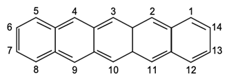
Figure 1. Carbon numbering of pentacene.
Unfortunately, pentacene is sensitive to ambient air (moisture and oxygen) and has low solubility, making it unstable when used with common fabrication techniques. Thus, pentacene should only be deposited using evaporation techniques. Initially, only ultra-high vacuum equipment was used in the deposition process for pentacene. Pentacene and its derivatives are not new materials. Nevertheless, they are still widely used in research and prototyping, either alone or in conjunction (stacked or blended) with other compounds.
The sensitivity of pentacene is due to its structure. This is because the diffusion of its five rings tempers the aromaticity and causes it to be more reactive [13]. This commonly occurs in the central ring, as the reaction of oxygen with the pentacene will produce an endo-peroxide on the central ring. Light and oxygen are the causes of this degradation and should be avoided during storage. These problems of solubility and stability were solved over the years through the development of two different methods [14].
The first method involves soluble pentacene precursors, as shown in Figure 2, which can be easily purified and deposited in solution form. This means that they are more soluble than the planar pentacene when deposited onto a substrate and can be converted into pentacene again using either heat or light. This process is called a retro-Diels–Alder reaction, which allows the precursors to be reconverted into semiconducting pentacene. This makes it competitive with other soluble semiconducting polymers, such as polypyrrole (PPy), polyaniline, and polydopamine (PDA).
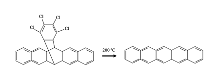
Figure 2. Example of a pentacene precursor structure.
The second method involves introducing substituents onto the aromatic core (Figure 3), which increases the stability and solubility of the pentacene. It can also improve the electrical properties due to the self-assembly of pentacene moieties, which causes them to be packed closely together. This method has better purity control and allows solution processing. It also improves the stability of the original pentacene against oxygen [15][16]. However, these pentacene derivatives cannot be converted back into pentacene in the way pentacene precursors can.
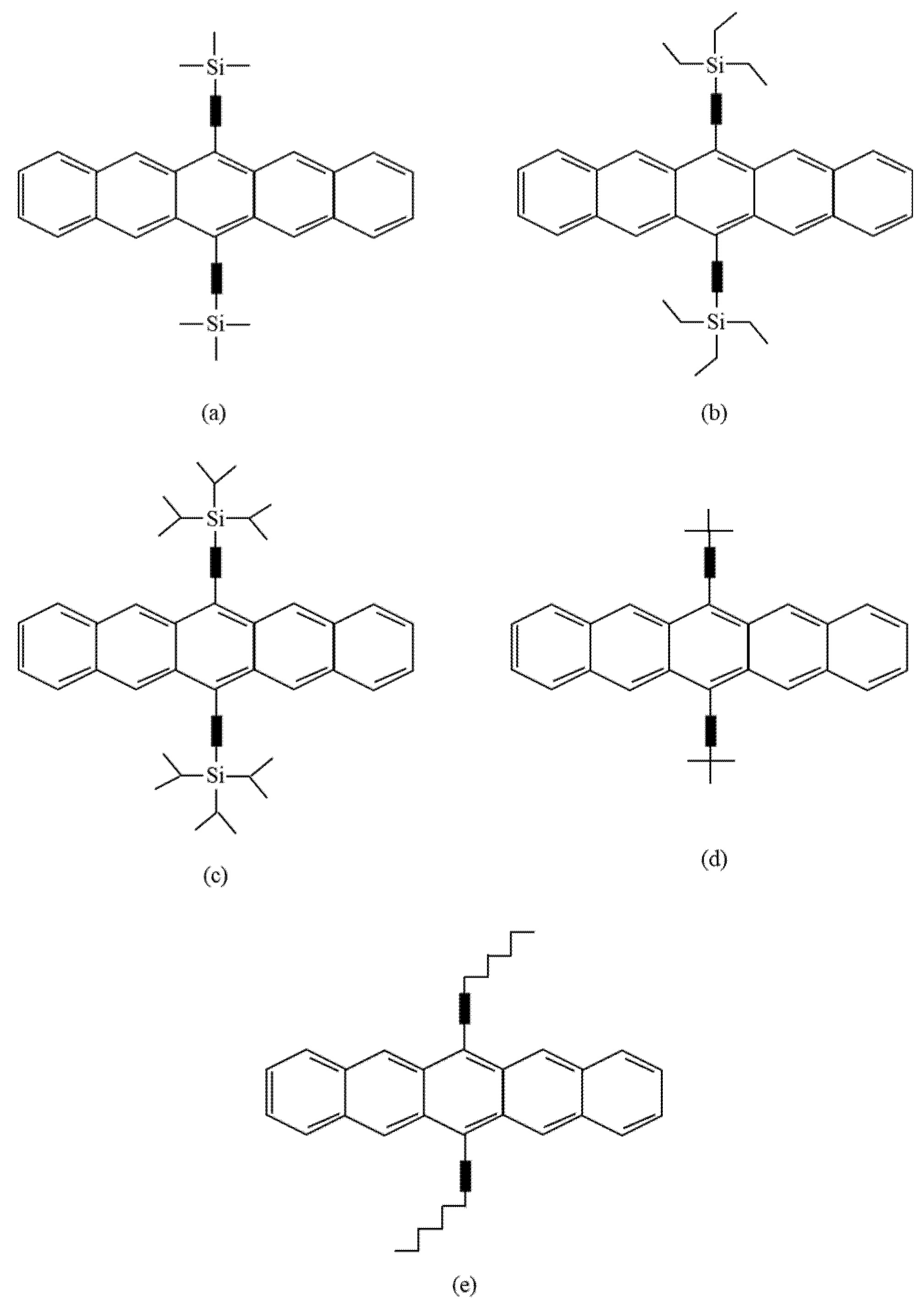
Figure 3. Structures of pentacene derivatives: (a) trimethylsilyl (TMS) pentacene; (b) triethylsilyl (TES) pentacene; (c) triisopropylsilyl (TIPS) pentacene; (d) t-butyl pentacene; (e) hexyl pentacene.
2.Thermal Vacuum Evaporation Methods
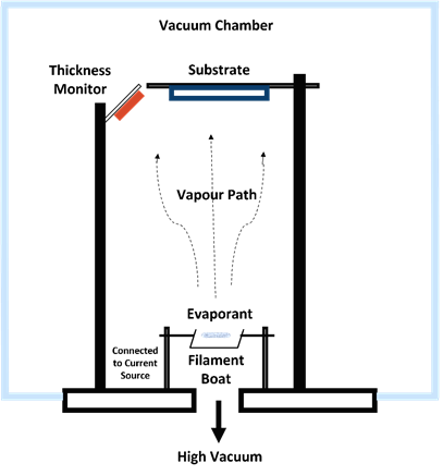
Figure 4. Thermal vacuum evaporation method.
The OVPD technique, however, uses a relatively low vacuum pressure combined with a carrier gas [24][25]. In this technique, the material is evaporated and the carrier gas transports the molecules out through an outlet and towards the substrate that has been placed underneath. This technique is illustrated in Figure 5.
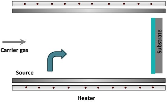
Figure 5. Organic vapor-phase deposition.
The performance results for other thermally evaporated OTFTs are listed in Table 1 [26][27][28][29][30]. Note that the table lists only the average typical values relevant to this manuscript. The typical mobility rate for pristine pentacene OTFT is around 1 cm2 V−1 s−1; much higher mobility values have been reported, it was required more complex treatments with mobility rates of up to 4.7 cm2 V−1 s−1 [27].
Table 1. Electrical performance comparison of OTFTs based on pentacene and its derivatives.
| Reference No. | Deposition Method | Material | Carrier Mobilities (cm2 V−1 s−1) |
ION/OFF | Threshold Voltage (V) |
|---|---|---|---|---|---|
| [31] | Thermal vacuum evaporation | TMS-pentacene, TES-pentacene, TIPS-pentacene, t-butyl-pentacene, hexyl-pentacene |
~10−5 ~10−5 0.4 10−4 No field conductivity |
NIL NIL 106 NIL NIL |
NIL |
| [26] | Thermal vacuum evaporation | Pentacene | 0.62 | 102 | −8.5 |
| Spin coating | Pentacene precursor of 13,6-N-Sulfinylacetamidopentacene (SAP), Pentacene precursor of 6,13-Dihydro-6,13-methanopentacene-15-one (DMP) |
0.031 0.09 |
103 | −12.5 −5 |
|
| [32] | Organic molecular beam | Pentacene | 0.435 | 1.83 × 10⁶ | 4.77 |
| [27] | Thermal vacuum evaporation | Pentacene | 2.5 | 107 | −4 |
| [28] | Thermal vacuum evaporation | Pentacene | 0.18 | 103 | NIL |
| [29] | Thermal vacuum evaporation | Pentacene | 0.1 | 3.3 × 10⁵ | 1.5 |
| [30] | Thermal vacuum evaporation | Pentacene | 0.025 | NIL | −1 |
| [33] | Spin coating | TIPS-pentacene | 0.002 | 102 | 3.2 |
| [34] | Spin coating | TIPS-pentacene | 0.005 | NIL | −1.3 |
| [35] | Spin coating | TIPS-pentacene | 0.6 | 106 | NIL |
| [36] | Spin coating | TIPS-pentacene | 1.66 | 7 × 10⁹ | NIL |
| [37] | Spin coating | TIPS-pentacene | 3.40 | 104 | −10 |
| [38] | Spin coating | TIPS-pentacene | 0.05 | NIL | NIL |
| [39] | Drop casting | TIPS-pentacene | 0.12 | 104 | −0.2 |
| [40] | Drop casting | TIPS-pentacene | 0.005 | NIL | 5 |
| [41] | Drop casting | TIPS-pentacene | 0.00016 | NIL | −10 |
| [42] | Drop casting | TIPS-pentacene | 0.57 | NIL | 0.27 |
| [43] | Drop casting | TIPS-pentacene | 2.22 | 1.3 × 10⁴ | −5.75 |
| [44] | Drop casting | TIPS-pentacene | 0.013 | NIL | −0.14 |
| [45] | Drop casting | TIPS-pentacene | 0.78 | 104 | −0.56 |
| [46] | Drop casting | TIPS-pentacene | 0.15 | NIL | NIL |
| [47] | Drop casting | TIPS-pentacene | 0.44 | 105 | −0.3 |
| [48] | Dip coating | TIPS-pentacene | 3.0 | 109 | 10 |
| [49] | Dip coating | TIPS-pentacene | 1.2 | NIL | NIL |
| [50] | Dip coating | TIPS-pentacene | 0.047 | NIL | NIL |
| [51] | Inkjet printing | TIPS-pentacene | 0.53 | 1.6 × 10⁶ | −0.7 |
| [52] | Inkjet printing | TIPS-pentacene | 0.23 | 2.01 x 10⁶ | NIL |
| [53] | Inkjet printing | TIPS-pentacene | 0.22 | 5.7 × 10⁴ | −0.4 |
| [54] | Inkjet printing | TIPS-pentacene | 0.35 | 1.2 × 10⁷ | NIL |
Other than the common OFETs and OLEDs, pentacene was also fabricated onto solar cells. Table 2 lists optoelectronic device performance comparisons. The thermal vacuum evaporation technique, devices are individually fabricated due to the limitations on space in the vacuum chamber. This deposition method is very costly, time-consuming, and not suitable for mass production. Hence, other deposition methods have been explored in order to solve these issues in the production process. The following alternative deposition methods, namely spin coating, dip coating, drop casting, and inkjet printing, are discussed in this manuscript.
Table 2. Performance comparison of pentacene-based optoelectronic devices.
| Reference No. | Deposition Method | Device | Material | Current Efficiency (Cd A−1) |
Power Efficiency (Im W−1) |
Turn On Voltage (V) |
Quantum Yield (%) | Power Consumption Efficiency (%) |
|---|---|---|---|---|---|---|---|---|
| [55] | Thermal vacuum evaporation | OLED | Pentacene | 6.6 | 3.4 | 5.8 | NIL | NIL |
| [56] | Thermal vacuum evaporation | Solar Cells | Pentacene | NIL | NIL | NIL | NIL | 0.33 |
| [57] | Thermal vacuum evaporation | Solar Cells | Pentacene | NIL | NIL | NIL | NIL | 5.7 |
| [58] | Thermal vacuum evaporation | OLED | Pentacene | NIL | NIL | 5.0 | 32 | NIL |
| [59] | Thermal vacuum evaporation | OLED | Pentacene | 3.4 | NIL | NIL | NIL | NIL |
3. Spin Coating Method
Spin coating is one of the most used methods, as well as in industry, due to its capability for mass production at cheaper costs [60][61][62][63]. It is also easier to perform as it only requires a few drops of solution. The solution is dropped on top of a substrate that is held onto a chuck within the spin coater, as illustrated in Figure 6. The spinning process starts with a certain acceleration rate and remains at a constant speed for a period of time. Upon completion, the desired thin film will form via a combination of evaporation processes and liquid flow. An additional step such as heat or UV treatment may be required depending on the solution’s characteristics [20].
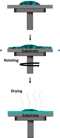
Figure 6. Spin coating method.
The surface coverage is important in this technique to ensure the uniformity of the thin film being deposited [64][65]. Bharti et al. [66] studied the deposition of TIPS-pentacene using this method with different dropping positions of the solution onto the substrate (Figure 7). They studied the effect it has on the alignment and crystallinity of the pentacene when it is deposited off-center to the substrate. Compared to the usual central dropping, the off-centered dropping approach was better for the crystallinity and pentacene alignment.
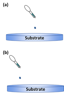
Figure 7. Illustration of the dropping positions: (a) central dropping; (b) off-centered dropping.
The thickness of the thin-film layer depends on the spin speed and duration of the spin. The solution’s properties, such as its density, viscosity, shear thinning, evaporation rates, and liquid flow, also effect the thickness. By altering the acceleration and spin speed, the liquid flow can be controlled. The evaporation rate on the other hand can majorly impact the morphology of the thin film. This method is suitably used to deposit pentacene precursors or pentacene derivatives, as they both are in solution form.
For TIPS-pentacene, the carrier mobility depends greatly on the crystal orientation [67][68][69], crystalline thickness, crystalline domain size, and presence of cracks. Past research had showed a mobility rate of 1.8 cm2 V−1 s−1 for TIPS-pentacene transistors [70][71]. This result depends on the solution concentration, solvent selection, temperature of the thermal treatment, method of deposition, and substrate material. In general, it has been shown that solvents with a high boiling point deliver slow crystal growth. This enables the thin film to be formed with a large lamellar structure, possibly giving higher mobility.
Although heat treatment is needed for complete solvent evaporation, temperatures above 60 °C could damage the thin-film organic semiconductor. For this reason, it is not easy to obtain devices with uniform characteristics. Hence, polymer blends were developed to improve the morphology of the TIPS-pentacene. Doing so enabled control of the crystallinity of the film, grain size, and other parameters.
In another related study, Wang et al. [36] investigated a low-viscosity organic semiconductor solution by spin coating a hydrophobic surface. Different solvents were tested to find the most suitable for producing a smooth, uniform, and continuous thin film. TIPS-pentacene was dissolved in hexane, toluene, chlorobenzene, 1,2-dichlorobenzene, and 1,2,3,4-tetrahydronaphthalene individually. Each solution was spin-coated onto an OTS/SiO2 substrate. They found that hexane produced the best results in terms of device performance. It improved the solution’s wettability by completely wetting the hydrophobic OTS/SiO2 surface.
The performance comparison of spin-coated OFETs are listed in Table 1.
4. Drop Casting Method
The drop casting method is an alternative deposition method that is more suitable for small-area deposition [73][74][75]. This method is performed by dropping a specified amount of solution on a static substrate and letting the solution evaporate for a desired amount of time. The substrate can also be baked to enhance the evaporation process. A solid thin film will then be formed on the substrate once the solution has dried up. The advantage of this method is its simple process. However, this method’s main disadvantages are the difficulty in obtaining a uniform and continuous coating on the deposited layer. The thickness of the deposited layer is also uncontrollable. Figure 8 shows an illustration of the drop casting method.
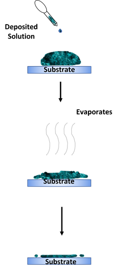
Figure 8. Drop casting method.
Park et al. [76] used this deposition method to learn terahertz modulation using a TIPS-pentacene thin film deposited on a patterned silicon substrate. The experiment was performed by drop casting 50 µL of TIPS-pentacene solution with a concentration of 2 mg/mL onto the substrate. It was then covered with a glass lid and heated on a 50 °C hotplate for 5 min. Despite the non-uniformity in the deposition process, the concentration of carriers injected into the TIPS-pentacene thin film rapidly became consistent over the whole area of the organic layer near the organic/inorganic interface. This was probably due to the fast in-plane diffusion of the carriers in the thin film itself.
Through the drop casting deposition method, the application of pentacene solutions for device fabrication has broadened from conventional OFETs to electrolyte-gated OFETs (EGOFETs). Lago et al. [44] reported the use of TIPS-pentacene as a high-performance biocompatible electronic device that can operate in water. Organic semiconductors such as pentacene have attracted interest and have been implemented in new applications due to their fascinating properties, including their flexibility, transparency, and low-cost processability. This deposition method, which is more affordable and simple, makes device fabrication a lot easier and more cost-efficient. In their study, they aimed to develop a biocompatible sensor, focusing on the stability of the device operation when in prolonged contact with a strong saline solution.
The performance comparisons of drop-casted OFETs are listed in Table 1.
It was highlight multiple flexible OTFTs and high-voltage OTFTs that were fabricated using the drop casting deposition method. This deposition method is mostly performed to learn the operational capability of such devices. The method is usually performed on a small substrate, avoiding the use of large amounts of materials, as the first step is usually just a draft of the device. There is no other force that influences the deposited droplet; hence, the crystal growth orientation is only influenced by the substrate’s surface tension. Although it produces seemingly good crystal growth and is suitable for the fabrication of flexible and conformable devices, the thin film’s uniformity is not guaranteed. The non-uniformity of the thin film causes the carrier mobility of the device to be low and similar to that of spin-coated thin films. Furthermore, it is not suitable for mass production. Similar to spin coating, this technique is also very vulnerable to contamination from oxygen reactions with the material and humidity, which can damage the material unless the process is performed in an inert environment.
4. Dip Coating Method
The dip coating method is also a commonly used technique, as it is fast and offers high uniformity when depositing thin-film layers [77][78][79]. The downside is that it requires a large amount of precursor solution in the reservoir. It is usually used to form thin films with complex and varying surface morphologies. It is conducted by suspending the substrate onto a clipper and then immersing it in the precursor solution below it. After a specified amount of time, the substrate will then be raised from the solution, enabling liquid film formation. It will then undergo an evaporation process that allows it to then form into a solid thin film. The thin film can then be processed further through thermal annealing or any other type of post-processing technique. Figure 9 shows an illustration of the dip coating method.
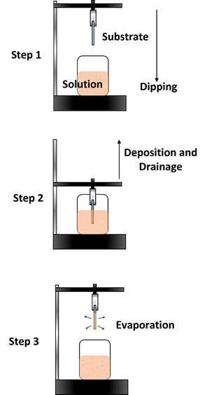
Figure 9. Dip coating method.
The increase or withdrawal speed of the substrate from the precursor solution determines the thickness of the thin-film layer. Other procedures can also be performed to alter the thickness of the thin film, such as varying the concentration of the precursor, the substrate temperature during the deposition, the acceleration rate, or even by performing the deposition at an angle [80–83]. However, it must be noted that several other forces influence the formation of the thin film, including the inertial forces, viscous drag, gravity, and the gradient of the surface tension [20].
It can be said that the dip coating deposition method does improve the continuity of the thin-film layer, which increases the uniformity of the thin film and results in less defects compared to the spin coating method. As discussed, this approach is preferable for various types of substrates that are flexible and irregular in shape, as this deposition method allows the solution to be spread over the substrate’s entire surface. The withdrawal speed is the main factor determining the thickness of the film. Other factors such as viscosity, liquid density, gravity, and surface tension can also influence the thickness. This is important, as a thin film’s thickness plays a role in enabling the carrier mobility flow. The withdrawal speed also influences the crystallinity growth of the thin film. Note that TIPS-pentacene was mainly used in the dip coating method. The crystalline growth of TIPS-pentacene thin films is important in producing a high carrier mobility rate. The optimum withdrawal speed and the type of solvent used when preparing the solution itself influence the formation of the thin film. This deposition method has shown much improvement as compared to the spin coating deposition method. However, this deposition method is not favorable due to the large volume of solutions used as the reservoir. This causes a lot of material waste, which conflicts with the aim of reducing the costs of the device fabrication process.
5. Inkjet Printing Method
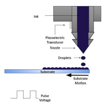
Figure 10. Inkjet printing method.
This method makes it possible for large-area deposition of various soluble materials. Since polymer blends have been known to overcome the difficulty of controlling crystal growth in soluble-processed TIPS-pentacene, as shown in [97], Cho et al. [51] investigated the behavior of TIPS-pentacene and amorphous polycarbonate (APC) in a polymer blend as the active layer using inkjet printing. Although the single-droplet inkjet printing of TIPS-pentacene with other polymer blends has been reported previously [98][99], the fabricated thin-film transistors showed issues in terms of film uniformity, especially when a geometrical parallel-type source drain was used, as the crystal orientation of the TIPS-pentacene in the single droplet was quite arbitrary.
The ratio of the blend was determined using the Flory–Huggins [100][101] and Cahn–Hilliard theories [102], whereby the Gibbs free energy when blending a polymer with TIPS-pentacene was evaluated. It is important to determine this ratio as it can affect the segregation strength between the TIPS-pentacene and the polymer phase. According to the theories, phase separation becomes easier with more positive Gibbs free energy values. In this study, the ratios were varied from 1:1 to 1:8 and were tested based on the OTFT performances. The highest mobility rate was obtained at 0.53 cm2 V−1 s−1 from the 1:4 ratio. This characteristic was observed to be closely related to the measurement of the phase separation strength between the TIPS-pentacene and the polymer phase. The crystal structures were then observed based on the various ratios. The crystals of inkjet-printed, non-blended TIPS-pentacene were highly anisotropic with various grain sizes, which led to a mobility rate of 0.22 cm2 V−1 s−1. The 1:1, 1:6, and 1:8 blended ratios produced plate-like wave crystalline structures with a random orientation, which resulted in carrier mobilities of 0.27 cm2 V−1 s−1, 0.35 cm2 V−1 s−1, and 0.17 cm2 V−1 s−1, respectively. Meanwhile, the 1:2 and 1:4 blended ratio produced stripe-shaped crystallite domains, resulting in carrier mobility rates of 0.46 cm2 V−1 s−1 and 0.53 cm2 V−1 s−1, respectively. This shows that the optimal TIPS-pentacene/APC mixing ratio induces strong phase separation and sequential crystal orientation, and it has a strong influence on the electrical properties of OTFTs.
The effect of the ink viscosity in wt.% on the device performance was examined [103]. The concentration was varied from 0.1 wt.% to 2.0 wt.% and it was found that the electrical performance of TIPS-pentacene/APC relied on the concentration as well as the viscosity of the inks. The average field-effect mobility seemed to increase from 0.04 cm2 V−1 s−1 to 0.53 cm2 V−1 s−1 when the concentrations were decreased from 2.0 wt.% to 1.0 wt.%. However, ink concentrations below 0.5 wt.% resulted in a lower mobility rate of 0.07 cm2 V−1 s−1 compared to the 1.0 wt.% and 1.5 wt.% concentrations at 0.53 cm2 V−1 s−1 (mentioned above) and 0.29 cm2 V−1 s−1, respectively. The inkjet-printed film with higher viscosity of 2.0 wt.% exhibited a broad and even distribution of TIPS-pentacene at all depth positions of the layer, with a slight occurrence of TIPS-pentacene at the top of the surface of the thin layer. The thin film with a 1.5 wt.% concentration showed a disconnected TIPS-pentacene layer in the top area, while at 1.0 wt.% the TIPS-pentacene was found to be discrete and showed a sharp phase separation in the upper area of the film. The OTFTs with the low-viscosity inks at 0.1 wt.% and 0.5 wt.% concentrations showed barely any distinguishable TIPS-pentacene layer at any position of the film, which meant that there were very small numbers of TIPS-pentacene crystals. Thus, ink viscosities lower than 0.5 wt.% does not produce a good OTFT performance.
Using the optimal ratio of 1:4, various solvents were tested for the TIPS-pentacene/APC solution, including toluene, toluene/chloroform, toluene/p-xylene, and toluene/tetralin. This was to investigate the effects of solvents on the field-effect mobility. The boiling point was the focus, as only 5 wt.% of the minor solvent was mixed with 95 wt.% of the major solvent (toluene), which was fixed. Toluene/p-xylene was shown to produce the highest mobility of 0.53 cm2 V−1 s−1 compared to toluene/chloroform, toluene, and toluene/tetralin, which exhibited carrier mobility rates up to 0.30, 0.31, and 0.40 cm2 V−1 s−1, respectively. This led to the observation of the thin films’ morphologies. It was shown that the Marangoni and convective flows of the drying ink are crucial for controlling the morphology of the inkjet droplets [104]. The high boiling point solvent, which was used as the major solvent, was mixed with a lower boiling point solvent, which was used as the minor solvent to control the evaporation rate of the droplets. As the evaporation rate increased at the edges of the droplets, this caused a buildup of convective flow from the center toward the drying edge of the droplets. This drove the surface tension gradient between the center and edge of the droplets. However, the opposing Marangoni flow arose in order to recirculate the solvents in the droplet. When the lower minor solvent boiling point was used, it produced a greater convective flow toward the drying edge, resulting in a higher edge wall of the droplet, which was known as the coffee ring effect. Thus, where a higher minor solvent boiling point was used, a weaker convective flow was created, with a smaller coffee ring effect. This behavior of the inkjet droplets influenced the morphology of the final printed thin film. Better-oriented TIPS-pentacene crystals were produced from the toluene/p-xylene solvents compared to the others. This also resulted in non-oriented large grain boundaries.
An important thing to mention is that the rest of the techniques discussed in this manuscript are all blanket deposition approaches, whereas the inkjet method is a “pattern” deposition approach, meaning that the deposition pattern can be produced in specific area with a specific shape, without using a mask or photoresist as the template. This offers a great advantage compared to other deposition methods and potentially reduces the fabrication steps and costs.
6. Conclusion
This manuscript compares various commonly used deposition methods that are associated with pentacene and its derivatives, including the classic thermal vacuum evaporation method, which is the initial method used for thin-film deposition. This approach uses pure pentacene in solid form to produce a uniform thin film, which results in good device performance. However, the disadvantage of this deposition method is the cost of the equipment and materials, as the specified amount of material can only be used in a single deposition process as compared to the soluble-process deposition method, where the same amount can be used for multiple depositions. This limits its production rate and output, as it is performed in a small vacuum chamber. For these reasons, when aiming to achieve low-cost fabrication at mass production rates, soluble process deposition methods are used. The commonly used soluble process deposition method in lab environment is the spin coating process. This is favorable as the cost of the equipment is not as expensive as the equipment used for thermal vacuum evaporation. It also does not require a large volume of source material to be used in its deposition process, which minimizes material waste. Hence, it is suitable for multiple device fabrication on a single substrate by using a small amount of source material. It forms a uniform thin-film layer, which can be enhanced with the use of surface treatments. The crystalline growth of the material in the thin film is also excellent, although the crystal orientation is highly influenced by the centrifugal force during the spinning process. This method has several disadvantages, as the outcome of the deposited layer is uncertain and is vulnerable to chemical reactions with the ambient environment. This issue is overcome by utilizing a glove box in an inert environment. The drop casting method is usually used for deposition on small substrates. It is preferable for the drafting of newly proposed devices and is suitable for flexible and conformable substrates. It has also been shown to produce good crystalline growth due to the small concentrated area involved. Nevertheless, the uniformity of the thin film itself is not guaranteed, as it is influenced by the gravitational force and the surface tension of the solution itself. This is a low-cost deposition method, as it uses only a small volume of material and is not normally used for mass production, which makes it a preferable method when it comes to new device structures or proposals. The dip coating method produces very uniform thin-film layers with good crystalline growth. This method is suitable for deposition on flexible and irregularly shaped substrates. The only downside of this deposition method is that it is not suitable for mass production, as it requires a large reservoir. This is costly and results in a large amount of material waste. Lastly, the inkjet printing method does not focus on the thin-film layer; instead, it forms a uniform and crystalline thin-film layer. This eliminates material waste as it uses the material in an efficient manner. It is suitable to use this method when a change of the device structure is the main variable in the study. Although the equipment is costly, it is well refined for the soluble process method and can also be used for mass production with high production speeds. The inkjet printing technology is mature, and thanks to this it can be integrated within organic electronics field. Every deposition method has its specified purposes, and they can be used according to their suitability for the desired device.

