Submitted Successfully!
To reward your contribution, here is a gift for you: A free trial for our video production service.
Thank you for your contribution! You can also upload a video entry or images related to this topic.
Version Summary Created by Modification Content Size Created at Operation
1 + 3429 word(s) 3429 2022-03-16 05:01:37 |
2 format corrected. + 111 word(s) 3540 2022-03-17 03:08:13 |

Video Upload Options

Do you have a full video?

Confirm

Are you sure to Delete?
Cite
If you have any further questions, please contact Encyclopedia Editorial Office.
Birowosuto, M.D. Hybrid Organic–Inorganic Perovskite Halide Materials for Photovoltaics. Encyclopedia. Available online: https://encyclopedia.pub/entry/20625 (accessed on 01 July 2024).
Birowosuto MD. Hybrid Organic–Inorganic Perovskite Halide Materials for Photovoltaics. Encyclopedia. Available at: https://encyclopedia.pub/entry/20625. Accessed July 01, 2024.
Birowosuto, Muhammad Danang. "Hybrid Organic–Inorganic Perovskite Halide Materials for Photovoltaics" Encyclopedia, https://encyclopedia.pub/entry/20625 (accessed July 01, 2024).
Birowosuto, M.D. (2022, March 16). Hybrid Organic–Inorganic Perovskite Halide Materials for Photovoltaics. In Encyclopedia. https://encyclopedia.pub/entry/20625
Birowosuto, Muhammad Danang. "Hybrid Organic–Inorganic Perovskite Halide Materials for Photovoltaics." Encyclopedia. Web. 16 March, 2022.
Hybrid Organic–Inorganic Perovskite Halide Materials for Photovoltaics
Edit

Hybrid organic–inorganic perovskite (HOIP) photovoltaics have emerged as a promising new technology for the next generation of photovoltaics since their first development 10 years ago, and show a high-power conversion efficiency (PCE) of about 29.3%. The power-conversion efficiency of these perovskite photovoltaics depends on the base materials used in their development, and methylammonium lead iodide is generally used as the main component. Perovskite materials have been further explored to increase their efficiency, as they are cheaper and easier to fabricate than silicon photovoltaics, which will lead to better commercialization. Even with these advantages, perovskite photovoltaics have a few drawbacks, such as their stability when in contact with heat and humidity, which pales in comparison to the 25-year stability of silicon, even with improvements are made when exploring new materials. To expand the benefits and address the drawbacks of perovskite photovoltaics, perovskite–silicon tandem photovoltaics have been suggested as a solution in the commercialization of perovskite photovoltaics. This tandem photovoltaic results in an increased PCE value by presenting a better total absorption wavelength for both perovskite and silicon photovoltaics.

power conversion efficiency hybrid perovskite tandem structure photovoltaics commercialization

1. Perovskite Tandem Photovoltaics

Perovskite tandem PVs have been suggested as a method to improve the overall performance, stability, and lifetime of perovskite PVs. A perovskite tandem PV usually consist of a cell—either silicon, perovskite, or copper indium gallium selenide (CIGS)—overlaid by a perovskite PV [1], to increase the efficiencies beyond a single junction limit [2], without adding a substantial cost during production [3][4]. Typical single-junction PV cells do not make use of 67% of the solar energy they receive, because of the weak absorbance capabilities of the semiconductors. Semiconductors can only absorb photons with energy is above their bandgap energy (Eg) and they generate energy equal to Eg, where the rest of the energy are lost through thermalization as heat. This will severely affect the PCE of a PV because it corresponds to the Voc and Jsc of the PVs. As one of solutions, tandem photovoltaics can address this problem [5].
Tandem PVs use stacks of materials with different bandgaps, where materials with larger bandgaps are put at the top of a cell and those with small bandgaps are at the bottom. High-energy photons are absorbed by the upper materials, while low-energy photons are not lost, in this case, but rather are absorbed by the lower stack materials, making use of most of the incident energy. One of the most known structures of tandem cells is the double-junction tandem device. They have two different configurations: two-terminal (2-T) and four-terminal (4-T) tandem, according to the stacking method used [5].
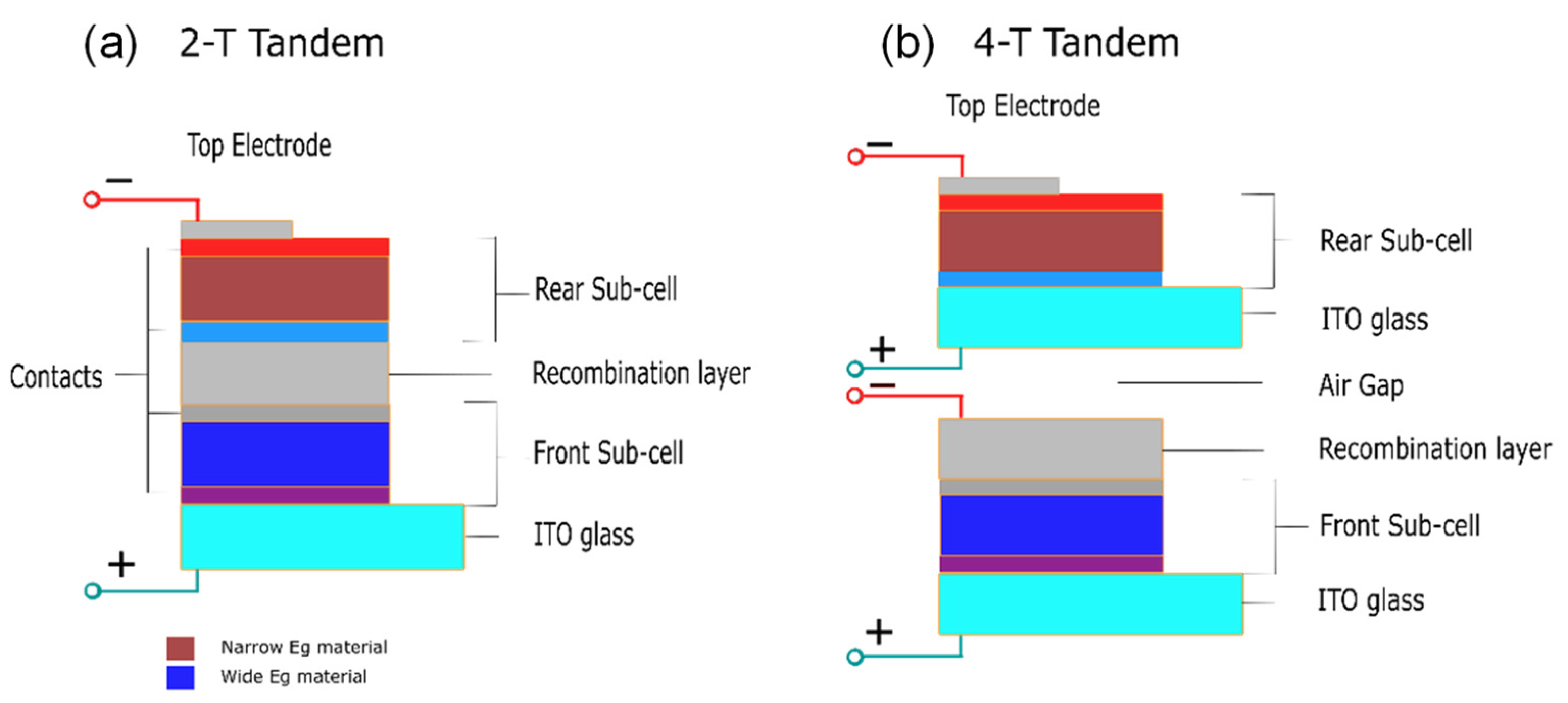
The 2-T tandem cells are synthesized by stacking a transparent front electrode, with a front cell and an opaque rear electrode, with the rear cell being one substrate where an interconnection layer (ICL) separates them, as shown in Figure 1a. The recombination of the photogenerated carriers from either sub-cell takes place in the ICL. On the other hand, 4-T tandem cells are made of two separate devices with two separate electrodes, linked together through a dichromatic mirror, as shown in Figure 1b. However, due to the additional electrodes, the optical loss will result in a more expensive cost compared to 2-T tandem PVs. Moreover, 2-T tandem PVs are cheaper to fabricate, though it is harder to fabricate 2-T or monolithic tandem PVs compared to 4-T tandem PVs for general applications [5].
Figure 1. Schematic diagram of (a) 2-T and (b) 4-T tandem perovskite.
Based on the values shown in Table 1, Voc, Jsc, and FF have similar in values with the 4-T Si/MAPbI3 configuration [6][7][8] and the values of Voc, Jsc, and FF in these works are about 1.1 V, 21 mA cm−2, and 75–80%, respectively.
Table 1. Some reports of perovskite tandem PVs. Voc, Jsc, and FF are open-circuit voltage, short-circuit current density, and fill factor, respectively.
Type Tandem Perovskite Material Voc (V) Jsc (mA cm−2) FF (%) Size (cm2) PCE (%) Ref.
4-T Si MAPbI3 1.08 20.6 74.1 0.075 23.0 [6]
4-T Si MAPbI3 1.098 21.0 74.1 1.10 26.7 [7]
4-T Si MAPbI3 1.156 19.8 79.9 1.00 27.0 [8]
2-T Si MAPbI3 1.69 15.9 77.6 0.17 21.2 [9]
2-T Si Cs0.05(FA0.77MA0.23)0.95Pb(I0.77Br0.23)3 1.87 19.37 79.9 1.06 29.3 [10]
2-T Si Cs0.05(MA0.17FA0.83)0.95Pb(I0.83Br0.17)3 1.792 19.02 74.6 1.088 25.2 [11]
2-T Si Cs0.15(MA0.17FA0.83)0.85Pb(I0.7Br0.3)3 1.80 17.8 79.4 ~1.00 25.4 [12]
4-T CIGS Cs0.09FA0.77MA0.14Pb(I0.86Br0.14)3 1.77 17.3 73.1 0.04 22.4 [13]
4-T CIGS Cs0.05(MA0.17FA0.83)Pb1.1(I0.83Br0.17)3 1.59 18.0 75.7 0.78 21.6 [14]
2-T CIGS Cs0.05(MA0.17FA0.83)0.95Pb(I0.83Br0.17)3 1.68 19.2 71.9 1.03 23.3 [15]
This occurs similarly in the 4-T CIGS/Cs0.05(MA0.17FA0.83)Pb1.1(I0.83Br0.17)3 configuration [14] and the 2-T CIGS/Cs0.05(MA0.17FA0.83)0.95Pb(I0.83Br0.17)3 configuration [15], since these works obtained similar values for Voc, Jsc, and FF of about 1.6–1.8 V, 17.0–19.2 mA cm−2, and 72.0–75.7%, respectively.
In comparison to the PCE values in Table 1, the 2-T configurations of CIGS/Cs0.05(MA0.17FA0.83)0.95Pb(I0.83Br0.17)3 [15][14] are better by 1.08-fold compared to those of the 4-T configurations. The 4-T configurations experience optical loss, which is found in the encapsulation and absorption in the transparent conductive electrode [16], which affects the PCE. The 2-T configurations experience series resistance loss in the large-area modules [17].
Further analysis is required to determine the increase in the PCE of the devices through development and improvements using tandem technologies. The configurations in Table 1 for tandem PVs refer to the materials in Table 2. The best performing PCE is from the Cs0.05(MA0.17FA0.83)(0.95)Pb(I0.83Br0.17)3 configuration in Table 2, and shows a PCE of 18.6% [18]; the best performing PCE from the 2-T Si/Cs0.05(FA0.77MA0.23)0.95Pb(I0.77Br0.23)3 configuration has a PCE of 29.3% [10] with an improvement achieved through tandem technologies using silicon and also through the use of an appropriate carbazole-based layer to efficiently extract the holes. Silicon was used as the bottom cell of the tandem since it has the properties of absorbing solar radiation from the near infrared region of the absorption spectrum. There is also another development in tandem PVs between Cs0.05(MA0.17FA0.83)0.95Pb(I0.83Br0.17)3 perovskite and CIGS, and the PCE value of the Cs0.05(MA0.17FA0.83)0.95Pb(I0.83Br0.17)3 tandem [15] increases by 1.25-fold compared to that of the intrinsic one [19].
Table 2. Various materials and methods for HOIP PV fabrications. Voc, Jsc, and FF are open-circuit voltage, short-circuit current density, and fill factor, respectively.
Coating Method Material Voc (V) Jsc (mA cm−2) FF (%) Size (cm2) PCE (%) Ref.
Spin-coating FAPbI3 1.06 24.7 77.5 ~1 20.2 [20]
Spin-coating Cs0.05(MA0.17FA0.83)(0.95)Pb(I0.83Br0.17)3 1.109 22.7 74.0 ~1 18.6 [19]
Spin-coating Cs0.1(MA0.17FA0.83)(0.90)Pb(I0.83Br0.17)3 1.13 22.0 77.0 ~1 19.1 [19]
Ink-jet printing Cs0.1(FA0.83MA0.17)0.9Pb(Br0.17I0.83)3 1.11 23.1 82 2.3 20.7 [21]
Spin-coating Cs0.15(MA0.17FA0.83)(0.85)Pb(I0.83Br0.17)3 1.088 19.4 69.3 ~1 14.6 [19]
Spin-coating (FAPbI3)0.95(MAPbBr3)0.05 1.14 24.9 81 ~0.094 23.2 [22]
Doctor blade MAPbI3 1.12 22.6 81 0.075 20.3 [23]
Doctor blade MAPbI3 1.10 22.7 81 0.08 20.2 [24]
Slot-die coating MAPbI3 1.03 22.1 74 ~232.3 16.8 [25]
Spin-coating MAPbI3 1.08 20.7 68 0.16 15.2 [26]
Ink-jet printing MAPbI3 1.08 22.66 76.2 0.04 18.6 [27]
Slot-die coating MAPbI3-xClx 1.06 21.7 ~78 0.06 18.0 [28]
Slot-die coating MAPbI3-xClx 1.09 22.38 74.7 0.096 18.3 [29]
Spray coating MAPbI3-xClx 1.10 21.4 77.6 0.08 18.3 [30]
Spin-coating MAPb(I0.85Br0.15)3 1.07 21.5 68 0.076 15.4 [31]
Spray-coating CsI0.05((FAPbI3)0.85(MAPbBr3)0.15)0.95 1.10 22.3 73 0.16 17.8 [32]
Screen printing (AB)2(MA)49Pb50I151 0.94 23.4 71 0.8 15.6 [33]
The CIGS allows for a tunable bandgap, and it varies based on the temperature. A tunable bandgap was obtained from 1.1 to 2.3 eV by interchanging the cations, metals, and halides. These allow for the tandem PV to absorb photons that have an energy above the bandgap, so a higher bandgap will require a higher energy for the absorption spectrum. The best configurations for perovskite tandem PVs came from silicon and CIGS. In fact, another perovskite–perovskite tandem PV has been recorded, with a high PCE of 24.4% [34] and there are few reports presently beating this record. Therefore, the best reported tandem perovskite photovoltaic belongs to the 2-T Si/Cs0.05(FA0.77MA0.23)0.95Pb(I0.77Br0.23)3 configuration with a PCE of 29.3% [10].
For further commercialization of perovskite PVs, large area modules should be developed since the previous studies were conducted for a small area (1 cm2). This development needs to be carried out to determine if there is any improvement in the crystal grain structure and PCE value when the module size is increased.

2. Large Scale Modules

Several issues need to be addressed for further perovskite PV commercialization: (i) a thin-film deposition method that is scalable and reproducible; (ii) high stability and long lifetime; and (iii) low or less toxic materials for large-area devices.
The rapid increment in PCE performance for perovskite PV has developed at a quick pace compared to other solar technologies. However, several high PCE values have been obtained with very small areas (~1.0 cm2). To fabricate a large area with a high-quality perovskite (good uniformity and few structural defects), several deposition methods have been developed, such as spin-coating, slot-die coating, doctor blade, and vacuum deposition. In 2015, Chen et al. [35] fabricated perovskite using one-step spin-coating with an active area of 1.02 cm2 and obtained a PCE of 15%. In 2016, Qiu et al. [36] fabricated a large-area perovskite with an active area of 1 cm2 and obtained a PCE of 13.6%.
While spin-coating is widely used in the deposition of small-area thin films in laboratories, it might not be suitable for industrial large-area fabrications. Spin-coated films are not uniform throughout the area [37], require a large amount of solution mixture of materials, and there is significant wasted solvent, which increases the cost of fabrication. Its performance also reduced due to the increase in series resistance and the decrease in film quality [38][39]. As in the case of Hossain et al. [40], since spin-coating is not suitable for the fabrication of perovskite solar cell on a silicon solar cell, so some methods have to be replaced by PVD or CVD.
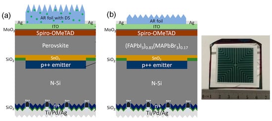
In 2018, Zheng et al. [41] were able to achieve 21.8% PCE using CVD on a 16 cm2 monolithic (FAPbI3)0.83(MAPbBr3)0.17 perovskite–silicon tandem PVs. The final product of the PVs has an enhanced Voc with a Jsc that ranged from 15.6 to 16.2 mA/cm2 and an FF of 78%. The supporting information regarding further improvements that could be achieved for this device would be the spiro-OMeTAD stack being replaced with a high refractive index inorganic hole transport layer to eliminate unnecessary wavelength absorptions. To improve it for commercial use in larger area of 6″ × 6″, the PDMS layer can be replaced with thin glass and the spin-coating process can be replaced with something less expensive, such as the doctor blade or spray-coating methods, which will be discussed in further works.
After conducting their previous work, in 2019, Zheng et al. [42] showed another improvement that increased the PCE value. They decided to use micron green-emitting (Ba,Sr)2SiO4:Eu2+ phosphor—a cheap material that is commercially available and is mostly used in light-emitting diodes—as an antireflective down shifting material on PDMS that acts as the hydrophobic layer of the silicon–perovskite tandem PVs with an area of 4 cm2, which achieved a PCE of 23%. SEM images of the (Ba,Sr)2SiO4:Eu2+ sample on PDMS showed a high-quality crystal size of about 10–20 μm. Moreover, the results of energy-dispersive X-ray spectroscopy (EDX), not only confirmed the homogeneous distributions of Sr, Ba, Si, and O within the specimen, but were also able to detect the Eu content. Figure 2 shows schematic diagrams of the (a) previous and (b) current large-scale modules of perovskite photovoltaics.
Figure 2. (a) Schematic of perovskite–silicon tandem homojunction photovoltaic with downshifting AR PDMS layer. From Ref. [42]. Copyright 2019 ACS Energy Letters. (b) Schematic of monolithic (FAPbI3)0.83(MAPbBr3)0.17 perovskite/rear-textured-homo-junction-silicon tandem photovoltaics. Reproduced with permission from Ref. [41]. Copyright 2018 ACS Energy Letters.
After further investigation, with a higher concentration of (Ba,Sr)2SiO4:Eu2+ phosphor on top of the perovskite–silicon PV, with initial conditions of Jsc of 14.1 mA/cm2, Voc of 1.73 V, FF of 82%, and a PCE of 20.1%, the result shows that, while the open-circuit voltage remains unchanged or at a constant level, there was an improvement in Jsc that was caused by the increased broad absorption of the cell with a reduced front reflection and increased light trapping. Eventually the best choice was obtained and had an area of 4 cm2 with conditions of Jsc of 16.4 mA/cm2, Voc of 1.73 V, FF of 81%, and a PCE of 23%.
Although works on monolithic perovskite–silicon tandem PVs showed progress in terms of PCE values (about 22–23%), there are several issues that need to be solved for further large-scale fabrication. These issues include stability improvements, the degradation rate, commercialization costs, and the use of environmentally friendly materials.

3. Improvements to Perovskite Material and Its Tandem Structures

A recent investigation, conducted by Green et al. [43] on perovskite–silicon tandem PVs, states that a high PCE value of 29.15% had been achieved with an area of 1.060 cm2. Though it is a small area, in the future, people will continue to develop perovskite–silicon tandem photovoltaics, which will progress further so that it is possible to achieve 4 cm2 perovskite–silicon tandem photovoltaic with an efficiency of 29.15%, if there is a breakthrough on how to further increase the broad absorption of a cell with reduced reflection but while increase the light trapping.
Furthermore, since it is difficult to deposit a large area of continuous perovskite film using the previously described traditional methods, other methods should be improved to prepare high-quality and large-area perovskite PVs for commercial production in the future. Moreover, from the perspective of green energy, the Pb employed in perovskite PVs is highly toxic, which will hinder the industrial promotion and development of perovskite PVs. Therefore, it is necessary to find a low-toxicity or non-toxic material to replace Pb in the future [44].
Realistically, the halide of Pb is 10 times more dangerous than the Pb that already exists on Earth [45][46][47][48]. Several lines of research indicate that contamination due to leaks of lead ions into soil and water resources is a permanent affliction and generates harmful effects on humans, animals, and plant survivability [49][50][51][52][53][54][55][56][57][58]. To decrease and reduce its toxicity level, Pb-free [59][60][61] (or at the very least less Pb content) perovskite–silicon PVs have been researched using a safer option by mixing chalcogen and halogen anions [62] or using tin or (Sn)-based perovskite PVs [63][64][65]. Recently, it was determined that there is an all-perovskite Pb–Sn tandem photovoltaic with a PCE of 26.4% [66], showing a value that potentially exceeds that of the best-performing single-junction perovskite solar cells, which are capable of retaining more than 90% of their initial performance after 600 h of operation at maximum power under one-sun illumination under ambient conditions. Recent research [67], developed a low-cost device made of sulfonic acid-based lead-adsorbing resin, which freezes lead ions into a scaffold and prevents their leakage when the perovskites are exposed to rainfall. This new device does not affect efficiency or scaling and the structure can be scaled up to 60.8 cm2.
However, Sn-based perovskite PVs have lower efficiencies and faster degradation than Pb-based perovskite PVs due to their phase fluctuations and they easily oxidize from Sn2+ to Sn4+. In the case of Sn-based perovskite PVs being unable to breach the efficiency limit of Pb-based perovskite PVs, new approaches had been created to prevent Pb leakage in perovskite PVs by trapping Pb with cation-exchange resins that are abundant in Ca2+ and Mg2+ [68].
In addition, the cost barrier for perovskite–silicon cells was identified as being due to expensive organic charge transport materials, such as spiro-OMeTAD, PTAA, and PC60BM [69][70][71][72]. The cost of organic charge transport, especially for one with a higher quality that can yield a better performance, is very expensive due to the intricate nature of the fabrication steps, in addition to the additional costs that might be derived from better or higher purity in terms of the formation of crystal grains. As an alternative to using organic charge transport materials, inorganic charge transport materials, such as NiO, CuSCN, SnO2, and Nb2O5, which are much cheaper in comparison to organic charge transport materials, have been successfully developed for some perovskite PVs [21][73][74][75].
Further improvements concern the degradation of the perovskite PVs. PVs are always exposed to various degradation sources, such as humidity, oxygen, heat, and ultraviolet light. To ensure the lifetime of perovskite–silicon tandem PVs, their stability needs to be tested and improved against degradation. Among perovskite PVs, methyl ammonium lead triiodide is easily degraded by humidity and heat, in comparison to perovskite PVs that are based on FAPbI3 [76] or CsPbI3 [77], which proved to have a higher resistance to thermal decomposition—which can be solved by mixing the cations and the halogen anions, which improves the thermal and crystal structure stability. As an example of mixing halide anions, bromide-based perovskite PVs show better resistance to degradation under humidity and heat when compared to iodide-based perovskite PVs as they developed a 2D or 3D hetero-structure in the perovskite PVs [78][79][80].
It is also suggested that organic charge transport materials, such as spiro-OMeTAD, PTAA, and PC60BM, are easily disintegrated by humidity and oxygen, so they require a higher level of encapsulation to prevent the elements from disintegrating the organic charge transport materials. An alternative solution would be to use inorganic charge transport materials, which are beneficial in terms of their stability due to their basic properties. In addition, a densely formed inorganic layer can act as a diffusion barrier to prevent organics or iodine species escaping from the lattice and reacting with the top metal electrode [81][82]. It has been reported in the literature that a semi-transparent perovskite PV with a dense charge transport layer and a transparent electrode endured through thermal cycling, damp heat, and UV stress tests 
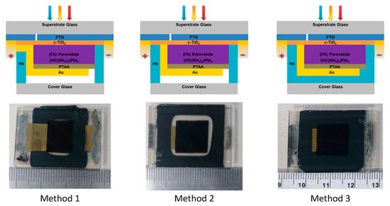
[81][82][83]. Moreover, low-temperature, glass–glass encapsulation techniques, using high-performance polyisobutylene (PIB) on planar perovskite solar cells, have been reported using three different electrical configurations and methods are as shown in Figure 3 [84]. In method 1, PIB is put on the top of a thin gold film that acts as a positive electrical feedthrough for the cell. In methods 2 and 3, the FTO layer provides the electrical feedthroughs. It is worth noting that the PIB in methods 1 and 2 plays the role of an edge seal, but it blankets the entire area under the glass in method 3.
Figure 3. Cross-sectional schematics with the photographs of perovskite solar cells encapsulated by three different methods [84]. From Ref. [84]. Copyright 2017 ACS Applied Materials and Interfaces.
Lead-free PVs are also being investigated as potential improvements to PVs [52][59], as these same materials were investigated as scintillators [85][86]. Several improvements regarding their material quality, degradation have been considered, as have techniques to fabricate them. To further improve the commercialization rate in the future, certain costs that are more expensive, such as organic charge transport materials, must be replaced. A better alternative would be the use of inorganic charge transport materials to reduce costs. While these methods will reduce the cost for commercialization, the most harmful content, which is the lead, will need to be replaced, reduced, or they will need to be made using Pb-free methods, discussed above, to reduce harm to the environment.
Several improvements have been achieved for perovskite–silicon tandem PVs, such as a longer lifetime, lower cost, and less-harmful chemicals being used. These achievements have inspired some companies to produce and commercialize perovskite–silicon tandem PVs.

4. Commercialization

For future commercialization, although there are several challenges to be faced in fabricating perovskite PVs, some companies are in the early stages of developing perovskite PVs, e.g., Saule technologies [87] and Quantum Solution [88]. These developments are driven by perovskite’s wide bandgap, low-cost, and simple fabrication methods. For Saule technologies, they launched the first industrial production line of solar panels in May 2021 in Poland, based on groundbreaking perovskite technology. They are making sheets of solar panels using a novel inkjet printing procedure invented by the founder, Olga Malinkiewicz [87].
However, the long-term performance of such a PV is an issue to pursue. As an example, the longest lifetime for the prototype was 6000 h under continuous one-sun illumination before degrading beyond 80% of its initial performance [89]. Interfacial recombination can be a severely degrading performance issue, but some methods are used to inhibit this. In [90], a 2D octyl-diammonium lead iodide interlayer was used to decrease recombination losses and obtain a PCE of 22.27% in tandem solar cells. A 2D/3D perovskite interface in [91] suppressed interface losses with a PCE ≈ 21%. As an alternative, perovskite–silicon tandem PV has a better lifetime of 300 h of operation, and retained 95% of its initial efficiency without encapsulant, and performs at a PCE of 29.3% in comparison to the theoretical limit of 29% for the silicon PV [92]. Therefore, the perovskite–silicon tandem PV is a prospective option for future commercialization; particularly, OxfordPV has pioneered producing their heterojunction silicon PVs to enhance their PV cells [93].

5. Summary

HOIPs have come a long way since their predecessors, with a current standing performance (or PCE) of about 29.3%. In this entry, the researchers highlighted the progress of HOIP materials and large-area fabrication techniques, in detail, and provided several comparisons between the techniques, and materials used in the fabrication of solar cells through their power conversion efficiencies. The fabrication techniques were also covered along with the advantages and disadvantages of using certain materials, which further enhance the properties of perovskite–silicon tandem solar cells; as shown using SEM. A scheme of this is shown in Figure 4, and it shows how far the progress of research towards commercialization and market must go. Although there has been feedback and improvements for materials, fabrication, characterization, and large-scale modules, commercialization is just starting. To enter the market of PVs, the other aspects, such as the total cost (although the material is cheap enough) and the aging of perovskite materials relative to those made using silicon, need to be addressed. Advances in other materials for optoelectronic devices such as graphene, MoS2 and compound semiconductors [94][95][96][97][98][99][100][101][102][103][104][105][106][107][108][109] are having a huge impact and benefitting the progress in the field of PVs either through the process techniques, or through the marketization strategies. In the end, the perovskite–silicon tandem solar cells have been introduced as the next generation of PVs and will replace the current technology of silicon PVs (in comparison of electric costs) [110].
Figure 4. Scheme of the progress of perovskite tandem PVs.

References

  1. De Vos, A. Detailed balance limit of the efficiency of tandem solar cells. J. Phys. D Appl. Phys. 1980, 13, 839–846.
  2. Shockley, W.; Queisser, H.J. Detailed Balance Limit of Efficiency of p-n Junction Solar Cells. J. Appl. Phys. 1961, 32, 510–519.
  3. Sofia, S.E.; Wang, H.; Bruno, A.; Cruz-Campa, J.L.; Buonassisi, T.; Peters, I.M. Roadmap for cost-effective, commercially-viable perovskite silicon tandems for the current and future PV market. Sustain. Energy Fuels 2019, 4, 852–862.
  4. Chen, B.; Ren, N.; Li, Y.; Yan, L.; Mazumdar, S.; Zhao, Y.; Zhang, X. Insights into the Development of Monolithic Perovskite/Silicon Tandem Solar Cells. Adv. Energy Mater. 2022, 12, 2003628.
  5. Wang, R.; Huang, T.; Xue, J.; Tong, J.; Zhu, K.; Yang, Y. Prospects for metal halide perovskite-based tandem solar cells. Nat. Photon. 2021, 15, 411–425.
  6. Chen, B.; Bai, Y.; Yu, Z.J.; Li, T.; Zheng, X.; Dong, Q.; Shen, L.; Boccard, M.; Gruverman, A.; Holman, Z.C.; et al. Efficient Semitransparent Perovskite Solar Cells for 23.0%-Efficiency Perovskite/Silicon Four-Terminal Tandem Cells. Adv. Energy Mater. 2016, 6, 1601128.
  7. Quiroz, C.O.R.; Shen, Y.; Salvador, M.; Forberich, K.; Schrenker, N.; Spyropoulos, G.D.; Heumüller, T.; Wilkinson, B.; Kirchartz, T.; Spiecker, E.; et al. Balancing electrical and optical losses for efficient 4-terminal Si–perovskite solar cells with solution processed percolation electrodes. J. Mater. Chem. A 2018, 6, 3583–3592.
  8. Wang, Z.; Zhu, X.; Zuo, S.; Chen, M.; Zhang, C.; Wang, C.; Ren, X.; Yang, Z.; Liu, Z.; Xu, X.; et al. 27%-Efficiency Four-Terminal Perovskite/Silicon Tandem Solar Cells by Sandwiched Gold Nanomesh. Adv. Funct. Mater. 2020, 30, 1908298.
  9. Werner, J.; Weng, C.-H.; Walter, A.; Fesquet, L.; Seif, J.P.; De Wolf, S.; Niesen, B.; Ballif, C. Efficient Monolithic Perovskite/Silicon Tandem Solar Cell with Cell Area >1 cm2. J. Phys. Chem. Lett. 2016, 7, 161–166.
  10. Al-Ashouri, A.; Köhnen, E.; Li, B.; Magomedov, A.; Hempel, H.; Caprioglio, P.; Márquez, J.A.; Vilches, A.B.M.; Kasparavicius, E.; Smith, J.A.; et al. Monolithic perovskite/silicon tandem solar cell with >29% efficiency by enhanced hole extraction. Science 2020, 370, 1300–1309.
  11. Mazzarella, L.; Lin, Y.-H.; Kirner, S.; Morales-Vilches, A.B.; Korte, L.; Albrecht, S.; Crossland, E.; Stannowski, B.; Case, C.; Snaith, H.J.; et al. Infrared Light Management Using a Nanocrystalline Silicon Oxide Interlayer in Monolithic Perovskite/Silicon Heterojunction Tandem Solar Cells with Efficiency above 25%. Adv. Energy Mater. 2019, 9, 1803241.
  12. Chen, B.; Yu, Z.J.; Liu, K.; Zheng, X.; Liu, Y.; Shi, J.; Spronk, D.; Rudd, P.N.; Holman, Z.C.; Huang, J. Grain Engineering for Perovskite/Silicon Monolithic Tandem Solar Cells with Efficiency of 25.4%. Joule 2019, 3, 177–190.
  13. Han, Q.; Hsieh, Y.-T.; Meng, L.; Wu, J.-L.; Sun, P.; Yao, E.-P.; Chang, S.-Y.; Bae, S.-H.; Kato, T.; Bermudez, V.; et al. High-performance perovskite/Cu(In,Ga)Se2 monolithic tandem solar cells. Science 2018, 361, 904–908.
  14. Jošt, M.; Bertram, T.; Koushik, D.; Marquez, J.A.; Verheijen, M.A.; Heinemann, M.D.; Köhnen, E.; Al-Ashouri, A.; Braunger, S.; Lang, F.; et al. 21.6%-Efficient Monolithic Perovskite/Cu(In,Ga)Se2 Tandem Solar Cells with Thin Conformal Hole Transport Layers for Integration on Rough Bottom Cell Surfaces. ACS Energy Lett. 2019, 4, 583–590.
  15. Al-Ashouri, A.; Magomedov, A.; Roß, M.; Jošt, M.; Talaikis, M.; Chistiakova, G.; Bertram, T.; Márquez, J.A.; Köhnen, E.; Kasparavičius, E.; et al. Conformal monolayer contacts with lossless interfaces for perovskite single junction and monolithic tandem solar cells. Energy Environ. Sci. 2019, 12, 3356–3369.
  16. Singh, M.; Santbergen, R.; Syifai, I.; Weeber, A.; Zeman, M.; Isabella, O. Comparing optical performance of a wide range of perovskite/silicon tandem architectures under real-world conditions. Nanophotonics 2021, 10, 2043–2057.
  17. Todorov, T.; Gunawan, O.; Guha, S. A road towards 25% efficiency and beyond: Perovskite tandem solar cells. Mol. Syst. Des. Eng. 2016, 1, 370–376.
  18. Habibi, M.; Ahmadian-Yazdi, M.-R.; Eslamian, M. Optimization of spray coating for the fabrication of sequentially deposited planar perovskite solar cells. J. Photon. Energy 2017, 7, 22003.
  19. Saliba, M.; Matsui, T.; Seo, J.-Y.; Domanski, K.; Correa-Baena, J.-P.; Nazeeruddin, M.K.; Zakeeruddin, S.M.; Tress, W.; Abate, A.; Hagfeldt, A.; et al. Cesium-containing triple cation perovskite solar cells: Improved stability, reproducibility and high efficiency. Energy Environ. Sci. 2016, 9, 1989–1997.
  20. Yang, W.S.; Noh, J.H.; Jeon, N.J.; Kim, Y.C.; Ryu, S.; Seo, J.; Seok, S.I. High-performance Photovoltaic Perovskite Layers Fabricated Through Intramolecular Exchange. Science 2015, 348, 1234–1237.
  21. Abzieher, T.; Moghadamzadeh, S.; Schackmar, F.; Eggers, H.; Sutterlüti, F.; Farooq, A.; Kojda, D.; Habicht, K.; Schmager, R.; Mertens, A.; et al. Electron-Beam-Evaporated Nickel Oxide Hole Transport Layers for Perovskite-Based Photovoltaics. Adv. Energy Mater. 2019, 9, 1802995.
  22. Jeon, N.J.; Na, H.; Jung, E.H.; Yang, T.-Y.; Lee, Y.G.; Kim, G.; Shin, H.-W.; Seok, S.I.; Lee, J.; Seo, J. A fluorene-terminated hole-transporting material for highly efficient and stable perovskite solar cells. Nat. Energy 2018, 3, 682–689.
  23. Deng, Y.; Zheng, X.; Bai, Y.; Wang, Q.; Zhao, J.; Huang, J. Surfactant-controlled ink drying enables high-speed deposition of perovskite films for efficient photovoltaic modules. Nat. Energy 2018, 3, 560–566.
  24. Wu, W.-Q.; Wang, Q.; Fang, Y.; Shao, Y.; Tang, S.; Deng, Y.; Lu, H.; Liu, Y.; Li, T.; Yang, Z.; et al. Molecular doping enabled scalable blading of efficient hole-transport-layer-free perovskite solar cells. Nat. Commun. 2018, 9, 1625.
  25. Di Giacomo, F.; Shanmugam, S.; Fledderus, H.; Bruijnaers, B.J.; Verhees, W.J.H.; Dorenkamper, M.S.; Veenstra, S.C.; Qiu, W.; Gehlhaar, R.; Merckx, T.; et al. Up-scalable sheet-to-sheet production of high efficiency perovskite module and solar cells on 6-in. substrate using slot die coating. Sol. Energy Mater. Sol. Cells 2018, 181, 53–59.
  26. Zhou, Y.; Yang, M.; Wu, W.; Vasiliev, A.L.; Zhu, K.; Padture, N.P. Room-Temperature Crystallization of Hybrid-Perovskite Thin FIlms via Solvent–Solvent Extractionfor High-Performance Solar Cells. J. Mater. Chem. A 2015, 3, 8178.
  27. Li, P.; Liang, C.; Bao, B.; Li, Y.; Hu, X.; Wang, Y.; Zhang, Y.; Li, F.; Shao, G.; Song, Y. Inkjet manipulated homogeneous large size perovskite grains for efficient and large-area perovskite solar cells. Nano Energy 2018, 46, 203–211.
  28. Whitaker, J.B.; Kim, D.H.; Larson, B.W.; Zhang, F.; Berry, J.J.; van Hest, M.F.A.M.; Zhu, K. Scalable slot-die coating of high-performance perovskite solar cells. Sustain. Energy Fuels 2018, 2, 2442–2449.
  29. Kim, Y.Y.; Park, E.Y.; Yang, T.-Y.; Noh, J.H.; Shin, T.J.; Jeon, N.J.; Seo, J. Fast two-step deposition of perovskite via mediator extraction treatment for large-area, high-performance perovskite solar cells. J. Mater. Chem. A 2018, 6, 12447–12454.
  30. Heo, J.H.; Lee, M.H.; Jang, M.H.; Im, S.H. Highly efficient CH3NH3PbI3−xClx mixed halide perovskite solar cells prepared by re-dissolution and crystal grain growth via spray coating. J. Mater. Chem. A 2016, 4, 17636–17642.
  31. Liu, M.; Johnston, M.B.; Snaith, H.J. Efficient planar heterojunction perovskite solar cells by vapour deposition. Nature 2013, 501, 395–398.
  32. Bishop, J.E.; Smith, J.A.; Greenland, C.; Kumar, V.; Vaenas, N.; Game, O.S.; Routledge, T.J.; Wong-Stringer, M.; Rodenburg, C.; Lidzey, D.G. High-Efficiency Spray-Coated Perovskite Solar Cells Utilizing Vacuum-Assisted Solution Processing. ACS Appl. Mater. Interfaces 2018, 10, 39428–39434.
  33. Hu, Y.; Zhang, Z.; Mei, A.; Jiang, Y.; Hou, X.; Wang, Q.; Du, K.; Rong, Y.; Zhou, Y.; Xu, G.; et al. Improved Performance of Printable Perovskite Solar Cells with Bifunctional Conjugated Organic Molecule. Adv. Mater. 2018, 30, 1706759.
  34. Lin, R.; Xiao, K.; Qin, Z.; Han, Q.; Zhang, C.; Wei, M.; Saidaminov, M.I.; Gao, Y.; Xu, J.; Xiao, M.; et al. Monolithic all-perovskite tandem solar cells with 24.8% efficiency exploiting comproportionation to suppress Sn(ii) oxidation in precursor ink. Nat. Energy 2019, 4, 864–873.
  35. Chen, W.; Wu, Y.; Yue, Y.; Liu, J.; Zhang, W.; Yang, X.; Chen, H.; Bi, E.; Ashraful, I.; Grätzel, M.; et al. Efficient and stable large-area perovskite solar cells with inorganic charge extraction layers. Science 2015, 350, 944–948.
  36. Qiu, W.; Merckx, T.; Jaysankar, M.; de la Huerta, C.M.; Rakocevic, L.; Zhang, W.; Paetzold, U.W.; Gehlhaar, R.; Froyen, L.; Poortmans, J.; et al. Pinhole-free perovskite films for efficient solar modules. Energy Environ. Sci. 2016, 9, 484–489.
  37. Yuan, Y.; Giri, G.; Ayzner, A.L.; Zoombelt, A.P.; Mannsfeld, S.C.B.; Chen, J.; Nordlund, D.; Toney, M.F.; Huang, J.; Bao, Z. Ultra-high mobility transparent organic thin film transistors grown by an off-centre spin-coating method. Nat. Commun. 2014, 5, 3005.
  38. Ding, B.; Li, Y.; Huang, S.-Y.; Chu, Q.-Q.; Li, C.-X.; Li, C.-J.; Yang, G.-J. Material nucleation/growth competition tuning towards highly reproducible planar perovskite solar cells with efficiency exceeding 20%. J. Mater. Chem. A 2017, 5, 6840–6848.
  39. Yang, M.; Zhou, Y.; Zeng, Y.; Jiang, C.-S.; Padture, N.P.; Zhu, K. Square-Centimeter Solution-Processed Planar CH3NH3PbI3Perovskite Solar Cells with Efficiency Exceeding 15%. Adv. Mater. 2015, 27, 6363–6370.
  40. Hossain, M.I.; Qarony, W.; Jovanov, V.; Tsang, Y.H.; Knipp, D. Nanophotonic design of perovskite/silicon tandem solar cells. J. Mater. Chem. A 2018, 6, 3625–3633.
  41. Zheng, J.; Mehrvarz, H.; Ma, F.-J.; Lau, C.F.J.; Green, M.A.; Huang, S.; Ho-Baillie, A.W.Y. 21.8% Efficient Monolithic Perovskite/Homo-Junction-Silicon Tandem Solar Cell on 16 cm2. ACS Energy Lett. 2018, 3, 2299–2300.
  42. Zheng, J.; Mehrvarz, H.; Liao, C.; Bing, J.; Cui, X.; Li, Y.; Gonçales, V.R.; Lau, C.F.J.; Lee, D.S.; Li, Y.; et al. Large-Area 23%-Efficient Monolithic Perovskite/Homojunction-Silicon Tandem Solar Cell with Enhanced UV Stability Using Down-Shifting Material. ACS Energy Lett. 2019, 4, 2623–2631.
  43. Green, M.; Dunlop, E.; Hohl-Ebinger, J.; Yoshita, M.; Kopidakis, N.; Hao, X. Solar cell efficiency tables (version 57). Prog. Photovolt. Res. Appl. 2020, 29, 3–15.
  44. Zhou, D.; Zhou, T.; Tian, Y.; Zhu, X.; Tu, Y. Perovskite-Based Solar Cells: Materials, Methods, and Future Perspectives. J. Nanomater. 2018, 2018, 8148072.
  45. Zhai, Y.; Wang, Z.; Wang, G.; Peijnenburg, W.J.G.M.; Vijver, M.G. The fate and toxicity of Pb-based perovskite nanoparticles on soil bacterial community: Impacts of pH, humic acid, and divalent cations. Chemosphere 2020, 249, 126564.
  46. Schileo, G.; Grancini, G. Lead or no lead? Availability, toxicity, sustainability and environmental impact of lead-free perovskite solar cells. J. Mater. Chem. C 2021, 9, 67–76.
  47. Su, P.; Liu, Y.; Zhang, J.; Chen, C.; Yang, B.; Zhang, C.; Zhao, X. Pb-Based Perovskite Solar Cells and the Underlying Pollution behind Clean Energy: Dynamic Leaching of Toxic Substances from Discarded Perovskite Solar Cells. J. Phys. Chem. Lett. 2020, 11, 2812–2817.
  48. Zhang, Q.; Hao, F.; Li, J.; Zhou, Y.; Wei, Y.; Lin, H. Perovskite solar cells: Must lead be replaced–And can it be done? Sci. Technol. Adv. Mater. 2018, 19, 425–442.
  49. Hailegnaw, B.; Kirmayer, S.; Edri, E.; Hodes, G.; Cahen, D. Rain on Methylammonium Lead Iodide Based Perovskites: Possible Environmental Effects of Perovskite Solar Cells. J. Phys. Chem. Lett. 2015, 6, 1543–1547.
  50. Li, J.; Duan, J.; Yang, X.; Duan, Y.; Yang, P.; Tang, Q. Review on recent progress of lead-free halide perovskites in optoelectronic applications. Nano Energy 2021, 80, 105526.
  51. Wang, R.; Wang, J.; Tan, S.; Duan, Y.; Wang, Z.-K.; Yang, Y. Opportunities and Challenges of Lead-Free Perovskite Optoelectronic Devices. Trends Chem. 2019, 1, 368–379.
  52. Giustino, F.; Snaith, H.J. Toward Lead-Free Perovskite Solar Cells. ACS Energy Lett. 2016, 1, 1233–1240.
  53. Shi, Z.; Guo, J.; Chen, Y.; Li, Q.; Pan, Y.; Zhang, H.; Xia, Y.; Huang, W. Lead-Free Organic-Inorganic Hybrid Perovskites for Photovoltaic Applications: Recent Advances and Perspectives. Adv. Mater. 2017, 29, 1605005.
  54. Yang, S.; Fu, W.; Zhang, Z.; Chen, H.; Li, C.-Z. Recent advances in perovskite solar cells: Efficiency, stability and lead-free perovskite. J. Mater. Chem. A 2017, 5, 11462–11482.
  55. Xu, P.; Chen, S.; Xiang, H.-J.; Gong, X.-G.; Wei, S.-H. Influence of Defects and Synthesis Conditions on the Photovoltaic Performance of Perovskite Semiconductor CsSnI3. Chem. Mater. 2014, 26, 6068–6072.
  56. Hoefler, S.F.; Trimmel, G.; Rath, T. Progress on lead-free metal halide perovskites for photovoltaic applications: A review. Monatsh. Chem. 2017, 148, 795–826.
  57. Lyu, M.; Yun, J.-H.; Chen, P.; Hao, M.; Wang, L. Addressing Toxicity of Lead: Progress and Applications of Low-Toxic Metal Halide Perovskites and Their Derivatives. Adv. Energy Mater. 2017, 7, 1602512–1602537.
  58. Ming, W.; Shi, H.; Du, M.-H. Large dielectric constant, high acceptor density, and deep electron traps in perovskite solar cell material CsGeI3. J. Mater. Chem. A 2016, 4, 13852–13858.
  59. Wang, M.; Wang, W.; Ma, B.; Shen, W.; Liu, L.; Cao, K.; Chen, S.; Huang, W. Lead-Free Perovskite Materials for Solar Cells. Nano-Micro Lett. 2021, 13, 62.
  60. Shalan, A.E.; Kazim, S.; Ahmad, S. Lead Free Perovskite Materials: Interplay of Metals Substitution for Environmentally Compatible Solar Cells Fabrication. ChemSusChem 2019, 12, 4116–4139.
  61. Zhou, J.; An, K.; He, P.; Yang, J.; Zhou, C.; Luo, Y.; Kang, W.; Hu, W.; Feng, P.; Zhou, M.; et al. Solution-Processed Lead-Free Perovskite Nanocrystal Scintillators for High-Resolution X-Ray CT Imaging. Adv. Opt. Mater. 2021, 9, 2002144.
  62. Hong, F.; Saparov, B.; Meng, W.; Xiao, Z.; Mitzi, D.B.; Yan, Y. Viability of Lead-Free Perovskites with Mixed Chalcogen and Halogen Anions for Photovoltaic Applications. J. Phys. Chem. C 2016, 120, 6435–6441.
  63. Zhang, X.; Wang, W.; Xu, B.; Liu, H.; Shi, H.; Dai, H.; Zhang, X.; Chen, S.; Wang, K.; Sun, X.W. Less-Lead Control toward Highly Efficient Formamidinium-Based Perovskite Light-Emitting Diodes. ACS Appl. Mater. Interfaces 2018, 10, 24242–24248.
  64. Soleimanioun, N.; Rani, M.; Sharma, S.; Kumar, A.; Tripathi, S.K. Binary metal zinc-lead perovskite built-in air ambient: Towards lead-less and stable perovskite materials. Sol. Energy Mater. Sol. Cells 2019, 191, 339–344.
  65. Shao, S.; Liu, J.; Portale, G.; Fang, H.-H.; Blake, G.R.; Brink, G.H.T.; Koster, L.J.A.; Loi, M.A. Highly Reproducible Sn-Based Hybrid Perovskite Solar Cells with 9% Efficiency. Adv. Energy Mater. 2017, 8, 1702019.
  66. Lin, R.; Xu, J.; Wei, M.; Wang, Y.; Qin, Z.; Liu, Z.; Wu, J.; Xiao, K.; Chen, B.; Park, S.M.; et al. All-perovskite tandem solar cells with improved grain surface passivation. Nature 2022, 603, 73–78.
  67. Chen, S.; Deng, Y.; Xiao, X.; Xu, S.; Rudd, P.N.; Huang, J. Preventing lead leakage with built-in resin layers for sustainable perovskite solar cells. Nat. Sustain. 2021, 4, 636–643.
  68. Chen, S.; Deng, Y.; Gu, H.; Xu, S.; Wang, S.; Yu, Z.; Blum, V.; Huang, J. Trapping lead in perovskite solar modules with abundant and low-cost cation-exchange resins. Nat. Energy 2020, 5, 1003–1011.
  69. Kim, C.U.; Jung, E.D.; Noh, Y.W.; Seo, S.K.; Choi, Y.; Park, H.; Song, M.H.; Choi, K.J. Strategy for large-scale monolithic Perovskite /Silicon tandem solar cell: A review of recent progress. EcoMat 2021, 3, e12084.
  70. Aitola, K.; Domanski, K.; Correa-Baena, J.-P.; Sveinbjörnsson, K.; Saliba, M.; Abate, A.; Grätzel, M.; Kauppinen, E.; Johansson, E.M.J.; Tress, W.; et al. High Temperature-Stable Perovskite Solar Cell Based on Low-Cost Carbon Nanotube Hole Contact. Adv. Mater. 2017, 29, 1606398.
  71. Kim, Y.; Jung, E.H.; Kim, G.; Kim, D.; Kim, B.J.; Seo, J. Sequentially Fluorinated PTAA Polymers for Enhancing V OC of High-Performance Perovskite Solar Cells. Adv. Energy Mater. 2018, 8, 1801668.
  72. Zhou, L.; Chang, J.; Liu, Z.; Sun, X.; Lin, Z.; Chen, D.; Zhang, C.; Zhang, J.; Hao, Y. Enhanced planar perovskite solar cell efficiency and stability using a perovskite/PCBM heterojunction formed in one step. Nanoscale 2018, 10, 3053–3059.
  73. Yang, I.S.; Sohn, M.R.; Sung, S.D.; Kim, Y.J.; Yoo, Y.J.; Kim, J.; Lee, W.I. Formation of pristine CuSCN layer by spray deposition method for efficient perovskite solar cell with extended stability. Nano Energy 2017, 32, 414–421.
  74. Yun, A.J.; Kim, J.; Hwang, T.; Park, B. Origins of Efficient Perovskite Solar Cells with Low-Temperature Processed SnO2 Electron Transport Layer. ACS Appl. Energy Mater. 2019, 2, 3554–3560.
  75. Feng, J.; Yang, Z.; Yang, D.; Ren, X.; Zhu, X.; Jin, Z.; Zi, W.; Wei, Q.; Liu, S. E-beam evaporated Nb2O5 as an effective electron transport layer for large flexible perovskite solar cells. Nano Energy 2017, 36, 1–8.
  76. Eperon, G.E.; Stranks, S.D.; Menelaou, C.; Johnston, M.B.; Herz, L.M.; Snaith, H.J. Formamidinium lead trihalide: A broadly tunable perovskite for efficient planar heterojunction solar cells. Energy Environ. Sci. 2014, 7, 982–988.
  77. Wang, K.; Jin, Z.; Liang, L.; Bian, H.; Bai, D.; Wang, H.; Zhang, J.; Wang, Q.; Liu, S. All-inorganic cesium lead iodide perovskite solar cells with stabilized efficiency beyond 15%. Nat. Commun. 2018, 9, 4544.
  78. Grancini, G.; Roldán-Carmona, C.; Zimmermann, I.; Mosconi, E.; Lee, X.; Martineau, D.; Narbey, S.; Oswald, F.; De Angelis, F.; Graetzel, M.; et al. One-Year stable perovskite solar cells by 2D/3D interface engineering. Nat. Commun. 2017, 8, 15684.
  79. Gharibzadeh, S.; Nejand, B.A.; Jakoby, M.; Abzieher, T.; Hauschild, D.; Moghadamzadeh, S.; Schwenzer, J.A.; Brenner, P.; Schmager, R.; Haghighirad, A.A.; et al. Record Open-Circuit Voltage Wide-Bandgap Perovskite Solar Cells Utilizing 2D/3D Perovskite Heterostructure. Adv. Energy Mater. 2019, 9, 1803699.
  80. Chen, P.; Bai, Y.; Wang, S.; Lyu, M.; Yun, J.-H.; Wang, L. In Situ Growth of 2D Perovskite Capping Layer for Stable and Efficient Perovskite Solar Cells. Adv. Funct. Mater. 2018, 28, 1706923.
  81. Cheacharoen, R.; Boyd, C.C.; Burkhard, G.F.; Leijtens, T.; Raiford, J.A.; Bush, K.A.; Bent, S.F.; McGehee, M.D. Encapsulating perovskite solar cells to withstand damp heat and thermal cycling. Sustain. Energy Fuels 2018, 2, 2398–2406.
  82. Cheacharoen, R.; Bush, K.A.; Rolston, N.; Harwood, D.; Dauskardt, R.H.; McGehee, M.D. Damp Heat, Temperature Cycling and UV Stress Testing of Encapsulated Perovskite Photovoltaic Cells. In Proceedings of the 2018 IEEE 7th World Conference on Photovoltaic Energy Conversion (WCPEC) (a Joint Conference of 45th IEEE PVSC, 28th PVSEC & 34th EU PVSEC), Waikoloa, HI, USA, 10–15 June 2018; pp. 3498–3502.
  83. Boyd, C.C.; Cheacharoen, R.; Bush, K.A.; Prasanna, R.; Leijtens, T.; McGehee, M.D. Barrier Design to Prevent Metal-Induced Degradation and Improve Thermal Stability in Perovskite Solar Cells. ACS Energy Lett. 2018, 3, 1772–1778.
  84. Shi, L.; Young, T.L.; Kim, J.; Sheng, Y.; Wang, L.; Chen, Y.; Feng, Z.; Keevers, M.J.; Hao, X.; Verlinden, P.J.; et al. Accelerated Lifetime Testing of Organic–Inorganic Perovskite Solar Cells Encapsulated by Polyisobutylene. ACS Appl. Mater. Interfaces 2017, 9, 25073–25081.
  85. Diguna, L.J.; Kaffah, S.; Mahyuddin, M.H.; Arramel; Maddalena, F.; Bakar, S.A.; Aminah, M.; Onggo, D.; Witkowski, M.E.; Makowski, M.; et al. Scintillation in (C6H5CH2NH3)2SnBr4: Green-emitting lead-free perovskite halide materials. RSC Adv. 2021, 11, 20635–20640.
  86. Hardhienata, H.; Ahmad, F.; Arramel; Aminah, M.; Onggo, D.; Diguna, L.J.; Birowosuto, M.D.; Witkowski, M.E.; Makowski, M.; Drozdowski, W. Optical and x–ray scintillation properties of X2MnCl4 (X = PEA, PPA) perovskite crystals. J. Phys. D Appl. Phys. 2020, 53, 455303.
  87. Malinkiewicz, O.; Yella, A.; Lee, Y.H.; Espallargas, G.M.; Graetzel, M.; Nazeeruddin, M.K.; Bolink, H.J. Perovskite solar cells employing organic charge-transport layers. Nat. Photon. 2013, 8, 128–132.
  88. Rong, Y.; Hu, Y.; Mei, A.; Tan, H.; Saidaminov, M.I.; Seok, S.I.; McGehee, M.D.; Sargent, E.H.; Han, H. Challenges for commercializing perovskite solar cells. Science 2018, 361, eaat8235.
  89. Krishna, A.; Zhang, H.; Zhou, Z.; Gallet, T.; Dankl, M.; Ouellette, O.; Eickemeyer, F.T.; Fu, F.; Sanchez, S.; Mensi, M.; et al. Nanoscale interfacial engineering enables highly stable and efficient perovskite photovoltaics. Energy Environ. Sci. 2021, 14, 5552–5562.
  90. Wang, D.; Guo, H.; Wu, X.; Deng, X.; Li, F.; Li, Z.; Lin, F.; Zhu, Z.; Zhang, Y.; Xu, B.; et al. Interfacial Engineering of Wide-Bandgap Perovskites for Efficient Perovskite/CZTSSe Tandem Solar Cells. Adv. Funct. Mater. 2021, 32, 2107359.
  91. Sutanto, A.A.; Caprioglio, P.; Drigo, N.; Hofstetter, Y.J.; Garcia-Benito, I.; Queloz, V.I.E.; Neher, D.; Nazeeruddin, M.K.; Stolterfoht, M.; Vaynzof, Y.; et al. 2D/3D perovskite engineering eliminates interfacial recombination losses in hybrid perovskite solar cells. Chem 2021, 7, 1903–1916.
  92. Hossain, M.I.; Qarony, W.; Ma, S.; Zeng, L.; Knipp, D.; Tsang, Y.H. Perovskite/Silicon Tandem Solar Cells: From Detailed Balance Limit Calculations to Photon Management. Nano-Micro Lett. 2019, 11, 1–24.
  93. Oxford, P.V. Tandem Cell Production. Available online: https://www.oxfordpv.com/tandem-cell-production (accessed on 10 August 2021).
  94. Samy, O.; Zeng, S.; Birowosuto, M.D.; El Moutaouakil, A. A Review on MoS2 Properties, Synthesis, Sensing Applications and Challenges. Crystals 2021, 11, 355.
  95. Samy, O.; Birowosuto, D.; El Moutaouakil, A. A Short Review on Molybdenum Disulfide (MoS2) Applications and Challenges. In Proceedings of the 2021 6th International Conference on Renewable Energy: Generation and Applications (ICREGA), Al Ain, United Arab Emirates, 2–4 February 2021; pp. 220–222.
  96. Samy, O.; El Moutaouakil, A. A Review on MoS2 Energy Applications: Recent Developments and Challenges. Energies 2021, 14, 4586.
  97. Tiouitchi, G.; Ali, M.A.; Benyoussef, A.; Hamedoun, M.; Lachgar, A.; Kara, A.; Ennaoui, A.; Mahmoud, A.; Boschini, F.; Oughaddou, H.; et al. Efficient Production of Few-Layer Black Phosphorus by Liquid-Phase Exfoliation. R. Soc. Open Sci. 2020, 7, 201210.
  98. Abed, J.; Rajput, N.S.; Moutaouakil, A.E.; Jouiad, M. Recent Advances in the Design of Plasmonic Au/TiO2 Nanostructures for Enhanced Photocatalytic Water Splitting. Nanomaterials 2020, 10, 2260.
  99. Moutaouakil, A.E.; Kang, H.-C.; Handa, H.; Fukidome, H.; Suemitsu, T.; Sano, E.; Suemitsu, M.; Otsuji, T. Room Temperature Logic Inverter on Epitaxial Graphene-on-Silicon Device. Jpn. J. Appl. Phys. 2011, 50, 070113.
  100. Moutaouakil, A.E. Two-Dimensional Electronic Materials for Terahertz Applications: Linking the Physical Properties with Engineering Expertise. In Proceedings of the 2018 6th International Renewable and Sustainable Energy Conference (IRSEC), Rabat, Morocco, 5–8 December 2018; pp. 1–4.
  101. Moutaouakil, A.E.; Suemitsu, T.; Otsuji, T.; Coquillat, D.; Knap, W. Nonresonant Detection of Terahertz Radiation in High-Electron-Mobility Transistor Structure Using InAlAs/InGaAs/InP Material Systems at Room Temperature. J. Nanosci. Nanotechnol. 2012, 12, 6737–6740.
  102. Moutaouakil, A.E.; Komori, T.; Horiike, K.; Suemitsu, T.; Otsuji, T. Room Temperature Intense Terahertz Emission from a Dual Grating Gate Plasmon-Resonant Emitter Using InAlAs/InGaAs/InP Material Systems. IEICE Trans. Electron. 2010, 93, 1286–1289.
  103. El Moutaouakil, A.; Suemitsu, T.; Otsuji, T.; Videlier, H.; Boubanga-Tombet, S.-A.; Coquillat, D.; Knap, W. Device Loading Effect on Nonresonant Detection of Terahertz Radiation in Dual Grating Gate Plasmon-Resonant Structure Using InGaP/InGaAs/GaAs Material Systems. Phys. Status Solidi C 2011, 8, 346–348.
  104. Hijazi, A.; Moutaouakil, A.E. Graphene and MoS2 Structures for THz Applications. In Proceedings of the 2019 44th International Conference on Infrared, Millimeter, and Terahertz Waves (IRMMW-THz), Paris, France, 1–6 September 2019; pp. 1–2.
  105. Moutaouakil, A.E.; Fukidome, H.; Otsuji, T. Investigation of Terahertz Properties in Graphene Ribbons. In Proceedings of the 2020 45th International Conference on Infrared, Millimeter, and Terahertz Waves (IRMMW-THz), Buffalo, NY, USA, 8–13 November 2020; pp. 1–2.
  106. El Moutaouakil, A.; Al Ahmad, M.; Soopy, A.K.K.; Najar, A. Porous Silicon NWs with FiTC-Doped Silica Nanoparticles. In Proceedings of the 2021 6th International Conference on Renewable Energy: Generation and Applications (ICREGA), Al Ain, United Arab Emirates, 2–4 February 2021; pp. 6–8.
  107. Moutaouakil, A.E.; Watanabe, T.; Haibo, C.; Komori, T.; Nishimura, T.; Suemitsu, T.; Otsuji, T. Spectral Narrowing of Terahertz Emission from Super-Grating Dual-Gate Plasmon-Resonant High-Electron Mobility Transistors. J. Phys. Conf. Ser. 2009, 193, 012068.
  108. Moutaouakil, A.E.; Suemitsu, T.; Otsuji, T.; Coquillat, D.; Knap, W. Room Temperature Terahertz Detection in High-Electron-Mobility Transistor Structure Using InAlAs/InGaAs/InP Material Systems. In Proceedings of the 35th International Conference on Infrared, Millimeter, and Terahertz Waves, Rome, Italy, 5–10 September 2010; pp. 1–2.
  109. Meziani, Y.M.; Garcia, E.; Velazquez, E.; Diez, E.; El Moutaouakil, A.; Otsuji, T.; Fobelets, K. Strained Silicon Modulation Field-Effect Transistor as a New Sensor of Terahertz Radiation. Semicond. Sci. Technol. 2011, 26, 105006.
  110. Chang, N.L.; Zheng, J.; Wu, Y.; Shen, H.; Qi, F.; Catchpole, K.; Ho-Baillie, A.W.Y.; Egan, R.J. A bottom-up cost analysis of silicon–perovskite tandem photovoltaics. Prog. Photovolt. Res. Appl. 2020, 29, 401–413.
More
Information
Subjects: Energy & Fuels
Contributor MDPI registered users' name will be linked to their SciProfiles pages. To register with us, please refer to https://encyclopedia.pub/register :
View Times: 512
Entry Collection: Organic Synthesis
Revisions: 2 times (View History)
Update Date: 17 Mar 2022
1000/1000
Video Production Service